Note: Descriptions are shown in the official language in which they were submitted.
21A~4~7
The present invention relates to a configurable
integrated circuit, with particular emphasis on a re-
configurable application specific device but without
limitation to same.
Micro-processors are designed into many
applications because of their low cost and high
performance. However, for many applications such as
image compression and digital signal processing they are
too slow. Modifications to the basic micro-processor
architecture has led to several new devices, digital
signal processors (DSP), reduced instruction set
computers (RISC) and custom processors (CP). Each of
these devices are optimised to perform a restricted
number of tasks but at very high speed. Many
applications require several types of such devices to
achieve the necessary level of performance. This is
because of the requirement to perform different types of
computational tasks over a period of time or the limited
capability of each device. Essentially these devices
are used as low cost high performance numerical engines,
each optimised to implement a general class of
algorithms. However, a designer frequently requires a
different architecture to efficiently implement a new
algorithm and the usual practice in such circumstances
is to design a custom processor for this task. This
leads to long and expensive design cycles and does not
- - 2142407
_
allow the designer any flexibility to change the
algorithm.
Field programmable gate arrays (FPGAs) are commonly
used to replace standard products and they could be used
as a numerical engine. However, they are general
purpose devices that cannot efficiently implement high
speed circuits. In order to achieve the level of
complexity that is normally required, several FPGAs
would be necessary which would increase the cost of the
final system. Some FPGAs are configured using on chip
static random access memory (SRAM) and these devices can
be re-programmed to perform different tasks which could
lead to greater flexibility and higher levels of
performance. However, these devices are connected to an
external source of configuration data that is accessed
by the device to configure internal resources. The
time to configure or re-configure the FPGA can be
several milliseconds, due to the necessity to import
configuration data from an external source, and this
time is several orders of magnitude too slow.
Reconfiguration speeds of less than 100 nano-seconds are
required for high performance applications. As such
FPGA's cannot be reconfigured fast enough to make them
suitable for use as a high performance numerical engine.
In FPGAs a considerable amount of silicon area is
committed to the configuration memory which is required
2142407
to program interconnect resources. Whilst in theory
FPGA's could accommodate an additional configuration by
increasing the amount of on chip memory which is
available to hold configuration data this would
probably increase the size of the chip by 60 per cent
which would be prohibitive for high density arrays.
The aim of the invention is to provide a re-
configurable architecture which can rapidly switch
between two or more, preferably several, configurations.
Another aim of this invention is to provide a device
that is specifically optimised to carry out functions
for numerically intensive applications. Another aim is
to provide a device that prior to the application of
power contains one or more boot up primary
configurations, suitable for configuring the device
into the intended application. A further aim is to
produce a device that has provision for passing data
between successive configurations of the (base) device.
A still further aim is to ensure that during
configuration of the device, data is held in a safe
condition and that switching currents are minimised. A
still further aim is to provide a configuration cache
that will allow updating of configuration memories that
are not currently in use. Another aim of the invention
is to allow the device to select its own configuration
from an external source of configuration data.
21424n~
-
Another aim is to reduce the number of
programmable interconnections by pre-wiring a portion of
the logic into the required configuration.
A yet further aim is to increase performance of
the device by pre-arranging specified primary functions
to specific areas of the device such primary functions
being substantially pre-wired.
Accordingly one aspect of the invention provides
a configurable semi-conductor integrated circuit in
which an area thereof is formed with a plurality of
cells each having at least one function and
interconnections with at least some other said cells, at
least some of the plurality of cells having
interconnections which are electrically selectable as to
their conduction state, and at least some of the
plurality of cells having interconnections which are
pre-wired, each cell has two or more possible
configurations, each configuration being defined by the
cell function and/or its interconnection with other
cells according to cell configuration data, and further
comprising means storing configuration data for at least
two cell configurations (per cell) and means to enable
one of the possible cell configurations according to the
cell configuration data selected.
By pre-wired in relation to interconnect we mean
uninterruptable as to its conduction state. The
- 2142A07
configuration data controls selection of the cell
function and/or cell interconnections preferably using
decoders or alternatively controlled directly from
memory. Thus for example the cells configuration data
determines the routing of the signal through the cell.
Direct connection paths exist between the configuration
stores, the decoders and the selectable functions and
interconnections. The term function as used herein may
be a logic function, arithmetic function, or
interconnect function. A cell may have one or more of
these functions or a combination of two or more of
these. Preferably the configuration data stores are
disposed in the cell. The desired configuration is
selected using an instruction bus receiving signals from
a sequencer and controller. One or more of the
configurations may be pre-wired (ie. not programmable).
Advantageously one or more of the configuration data
stores are programmable using a data transfer bus.
Where more than one store is programmable an instruction
update bus is provided to write enable the required
configuration store. Configuration stores not currently
accessed to control interconnection and/or cell function
can be updated using the instruction update bus.
Since the present invention is particulary
concerned with an application specific device which is
optimised to perform a restricted number of tasks at
- 2142~07
high speed but which is quickly reconfigurable during
program execution (when required) to perform some other
specific task, cells are optimised for a primary
function according to a primary configuration.
Advantageously the primary configuration data is pre-
wired. It is convenient to have two alternate pre-wired
primary configurations. Cells can be and most usually
will be optimised for different primary functions.
Advantageously the pre-wired interconnections are used
in connection with the optimised functions.
A possible primary function is that of an adder.
Another aspect of the invention provides a multi-bit
adder for summing at least two multi-bit words
comprising a first multi-bit adder block for summing the
least significant bits and at least one further multi-
bit adder block for summing the most significant bits
and having sum selection means wherein said further
multi-bit adder block calculates the two possible sums
resulting from a carry out from the previous block being
equal to 'O' and '1' respectively and wherein the sum
selection means selects the sum of the further multi-bit
adder block according to the carry out calculated from
the previous block.
In the case of a Digital Signal Processor
application, some cells will be optimised as Arithmetic
Logic Units (ALU) while other cells may be optimised to
2142407
carry out functions such as instruction decode or as
processor registers. The number of different cells is
only limited by the size of the array of cells. In
practice the array will be divided into a number of
discrete areas that are particularly efficient at
implementing respective primary functions. It will be
apparent that each of these cells has the capability to
implement another function and usually a range of other
functions according to other configurations. These
additional functions are controlled by the controller
and sequencer whose role is to ensure that the correct
function is available when required. Primary functions
may use general interconnect resources, but preferably
they have their own dedicated resource for high speed
connections between primary functions of other cells.
In this way the performance of the device is not
dependent on a general programmable interconnect
resource and by connecting primary functions through
resources with smaller parasitic loads, the device can
operate faster.
In order to safeguard data when changing between
configurations each cell has a latch controlled by a
function control bit. Transient current is reduced when
switching between configurations by the provision of a
buffer in each cell, the buffer being controllable as
to is state during reconfiguration by a control line.
- 2142407
It will be apparent that whilst this device has
specific application in the field of numerical engines
such as DSP's, the primary functions can be chosen to
suit other applications. Accordingly the techniques can
be applied to any application. For example, another
application is as a programmable communications device.
Another aspect of the invention also provides a
method of configuring a configurable semi-conductor
integrated circuit in which a sequence is programmed
with data to facilitate selection of a required
configuration from at least two possibilities. Usually
each of a plurality of cells will have at least two
configuration possibilities. Advantageously the
configurations are programmable and the method further
comprises inputting and storing configuration data. A
further advantageous feature is the ability to program
the sequences to write over previously stored
configuration data at a prescribed point in operation of
the circuit. An aspect of the invention provides a
semi-conductor integrated circuit in which the circuit
configuration is changed according to a pre-programmed
sequence of configuration during operation of the
device.
The present invention will now be described by
way of example only with reference to the accompanying
drawings; in which:-
2 1 424~
Figure 1 is a schematic layout for re-
configurable application specific device embodying the
invention;
Figures 2 and 3 illustrate diagrammatically the
feature of the core architecture having different
configurations and sequential access;
Figure 4 illustrates diagrammatically the feature
of the core having cells which are optimised to
implement specific functions;
Figure 5 illustrates diagrammatically a primary
configuration for the device as a Digital Signal
Processor (DSP);
Figure 6 illustrates diagrammatically a secondary
configuration for the device as a large multiplier;
Figure 7 illustrates schematically the layout of
a cell including configuration memory means;
Figure 8a illustrates diagrammatically the
possible arrangement of the cells in blocks with
optimised functions;
Figure 8b illustrates schematically programmable
local and global interconnect resources for the cells;
Figures 9a and 9b illustrate diagrammatically how
the global interconnect resources are connected to the
cell input and output multiplexers;
Figures sc and sd illustrate diagrammatically an
array of cell blocks and the arrangement of cells within
. 21424P7
a cell block;
Figure 10 illustrates diagrammatically cell
output state control;
Figures 11, 12 and 13 illustrate diagrammatically
three logic cell variants namely an Arithmetic Logic
Unit function (ALU), an Accumulator function (ACC), and
a Decode cell function respectively;
Figure 14 illustrates diagrammatically examples
of different functions from the ALU and ACC optimised
core cells;
Figure 15 illustrates diagrammatically details of
configurable Static Random Access Memory provisions;
Figure 16 illustrates diagrammatically further
details of the cell configuration memory;
Figure 17 illustrates diagrammatically
instruction bus connections for DSP cells;
Figure 18 illustrates diagrammatically a novel
parallel carry select adder architecture which can be
configured by the device;
Figure 19 illustrates a cell configured to
implement a single stage carry select adder;
Figure 20 illustrates a cell configured to
implement two carry select adders;
Figure 21 illustrates an alternative cell
configuration to implement a single stage carry select
adder; and
_ 2142407
Figure 22 illustrates diagrammatically a DSP
Timing Diagram.
The present invention is described in the context
of an integrated circuit intended for an application
specific device and will be described by way of example
in the specific context of a Digital Signal Processor
(DSP). According to the invention the device is not
restricted to a fixed architecture, but has the hardware
re-configurable to allow the device (eg. DSP) to be
optimised for each individual task. Thus at a macro
level the device may be optimised for a new application
for example MPEG, Polygon Engine, Blitter, DMA Engine,
whilst at a micro level, the device can be optimised for
each OPCODE, eg. MULTIPLE ALU, CUSTOM MULTIPLY. Thus a
re-configurable application specific device (eg. DSP)
allows many custom devices to be replaced with a single
chip. Optimised OPCODES increase performance. In
effect the device can switch at clock speed between
operating as a DSP, RISC or custom processor.
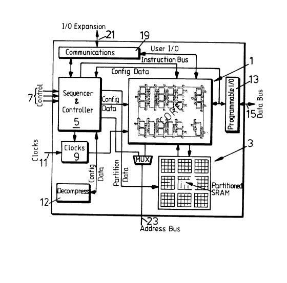
Referring firstly to Figure 1, here there is
illustrated a re-configurable application specific
digital signal processor. The chip includes an area 1
of core cells, Partitioned Static Random Access Memory
(SRAM), 3, a sequencer and controller 5 having control
lines 7, clocks 9 and clock lines 11, as well as
programmable input/output 13 and associated data bus
21424Q~
14
15. Also shown is a signal Decompress decoder 17, a
communications link 19 and associated input/output and
Expansion porting 21, and address bus 23.
There are a plurality of core cells 2 and these
provide for example (in the case of a DSP
configuration), Instruction Decode, registers, programme
counter and stack pointer facilities. Each core cell
can be programmed to perform a range of functions and
certain core cells are optimised to implement specific
functions. Thus, for example, reference to Figure 4
illustrates optimisation of certain cells for ALU
functions as at 2a, registers 2b, programme counter 2c,
general counter 2d, instruction decode 2e and
input/output 2f.
One schematic configuration of core cell denoted by
dotted outline is shown in Figure 7 and the core cell
includes within it a logic cell 22 having selectable
functions (for example four). Programmable core cell
inputs (eight) (ie. electrically selectable
interconnections) are shown at 25 applied to two 4:1
input multiplexers 26,28. The cell output is shown at
27. Examples of Logic cell configurations are described
further with reference to Figures 11, 12,13, and 14.
Input multiplexers are controlled by respective 2-4
Decoders 30, 32. A further 2-4 Decoder 34, controls a
4-1 Multiplexer in the logic cell 22 and an output
_ 21424~7
multiplexer 70 is controlled by a 2-4 Decoder 48.
Direct pre-wired connections to the logic cell are
indicated by numeral YA-YD.
In the Figure 7 illustration the cell includes
configurable memory provisions comprising configuration
cache 36 and instruction cache 38, as well as so called
"hard wired" or fixed configuration provisions 40. For
the DSP application the fixed configurations comprise a
primary DSP Boot Configuration set by 3 x 2 bit
configuration elements 40a, and a secondary
configuration eg. Multiplier configuration set by 3 x 2
bit configuration elements 40b. It is intended that the
primary (fixed) configuration will be implemented
automatically on boot-up of the device so as to give it
its primary application specific function.
The configuration cache 36 in the illustrated
embodiment comprises four, 3 x 2 bit data stores, 36a-d
which can be write enabled from an instruction update
bus 44 and written with data from Data bus 46. The
instruction cache 38 comprises 8 x 2 bit data stores
which are write enabled from the Instruction update bus
(44) and written with data from the data bus 46. The
instruction cache 38 is read enabled from the
Instruction select bus 42. A 2-4 Decoder 48 enabled
from the instruction select bus 42 selects and read
enables one of the four data stores 36a-d according to
- 21424~7
16
the data store of the instruction cache selected. The
output of Decoder 48 also facilitates the direct
configuration of the logic cell by controlling the 4:1
output multiplexer 70. Also illustrated is a function
control bit 50 and has connections from the read and
write enable lines (42,44) and into the logic cell 22.
The function control bit 50 controls latch 54 (see
Figure 10).
Figure 16 illustrates, for the fixed configuration
provisions (40) and the configuration cache 36, the read
(42), write 44' and data 46' connections. Note both
read and write provisions for the configuration cache 36
only.
Reverting back to Figures 2 and 3, each of blocks
2', 2'' and 2''' represent configurations of the core 2.
Large blocks of functionality are accessed as a series
of configurations. Each new configuration receives
data from the last using inter-process connections 52
and cells 54 designated for latching critical data.
Other cells 54 are designated to act as inputs or
outputs. Reconfiguration time can be of the order of
10nsec. The core architecture is optimised to implement
each OPCODE. This allows the word size of each
arithmetic function to be adjusted to the required
provision. Thus, referring to Figure 3, a first core
configuration (OPCODE 1) executes a 16 bit multiply and
21424Q'r
cos function, a second core configuration (OPCODE 2)
carries out a 32 x 32 bit multiply function, and a third
configuration (OPCODE 3) carries out a 64 bit ADD
function.
Reference is now made to Figure 10 which
illustrates the output state control as applicable to
the like of the cell illustrated in Figure 7 and the
corresponding cell components appropriately referenced
are illustrated with the exception of the instruction
cache 38.
As has been mentioned above certain cells are
designated for latching critical data and hence the
cells have a latch provision 54 with inputs from the
function control bit 50 and a hold input line 56. These
function to preserve the state of data from cells
between configurations. In addition a buffer 60 is
provided in order to reduce transient current when
switching between configurations by setting its output
state to a known condition.
The cells interconnect resources are now described
with reference to Figures 8a, 8b, 9a, and 9b. Figures
8a and 8b show diagrammatically how cells might be
arranged in regular blocks (B) (eg. rows and columns),
with the blocks including cells which are optimised for
different functions. Thus Figure 8b shows columns of
ACC cells, ALU cells and shift cells, and two rows of
21~2407
_,
18
Decode cells. Columns of cells each have two global (Y)
buses (Y1, Y2, Y3, Y4....... YN1, YN) and the rows of
cells each have at least two global (X) buses (X1,
X2...... Xn-l, Xn). The Decode cells head up the columns
of each block and have three X buses. Bus switches BS
are provided in the Y buses between adjacent blocks. In
addition there are hidden (or pre-wired direct
connection) Y buses, YA-YD. These run from the decode
cells to all the cells in the column below. In addition
local direct connection paths are preferred between
cells. Thus, taking as an example cell SC in Figure 8b,
it has input connections from outputs of an upper
adjacent cell, a lower adjacent cell, a right adjacent
cell, a left adjacent cell, and a next left adjacent
cell. These connections are designated U, D, R, L, J.
Not all cell variations will necessarily have all the
local connections. The majority of these local
connections are electrically selectable as to their
conduction state, but most usually the left adjacent
connection will be a pre-wired connection.
Figure 9a illustrates, for one cell as for all
core cells, how an input multiplexer 26 controls
selection of inputs from X and Y buses and an output
multiplexer 70 controls selection of outputs to the same
X buses and next column of Y buses.
The cells are arranged in 10 x 8 blocks and an
- 2i424~7
19
example of such an array of cell blocks is illustrated
in Figure 9c. Blocks 100 are formed in an 8 x 4 array
and a programmable input/output 102, data buses and
switches 104 and partitioned SRAM 106 are also shown.
Each block 100 comprises an array of 10 x 8 cells and
conveniently, columns of cells within the block have a
similar primary configuration. For example, Figure 9d
illustrates a block 100 having two columns of cells 100
a & b configured as multiplexer cells, columns 100 c as
a product adder, lOOd barrel shifter cells, 100 e
arthimetic and logic cells, 100 f accumulator cells and
columns 100 g & h configured as multiplier expansion
cells. The columns in each block are headed up by
decode cells.
Referring now to Figure 15, the configurable
static random access memory (SRAM) 3 stores partition
data passed to it from the sequencer and controller 5
along partition data bus 72. The operation of the DSP
requires the storing and retrieving of data and the
provision of the SRAM on the device ensures that access
to the stored data is faster than if the SRAM was
located externally.
The sequencer and controller 5 controls the
operation of buses 42, 44, 45 and 46. Hence, the
sequencer and controller 5 includes the control of the
operation of selecting individual data stores of cells,
_ 2142~7
sending data to the stores and controlling the sequence
of implementation of configuration data stored within
cell. The necessary control instructions for the
sequencer and controller 5 is provided by an external
source of memory (not shown). In addition to the above
operations, the controller 5 can select individual data
stores not currently used such that they can be updated
with new configurations from the external memory.
Figures 11, 12 and 13 illustrate respective ALU,
ACC and Decode cell variants. Appropriate references
have been used as previously referred to.
Figure 13 shows an example of a cell optimised
for decode. Two decode cells will head up the blocks of
cells as shown in Figures 8a and 8b. The illustrated
variation is the one which has the pre-wired
interconnection YA, YB which feed down to each of the
cells below. The other decode will generate the YC, YD
pre-wired interconnections. Thus the ALU type cells of
Figure 11 have pre-wired connections YA, YB, whilst the
ACC type cells have pre-wired connections YA, YB, YC,
YD. Note also that for the ALU and ACC variants the
left adjacent connection L is pre-wired, and for the ALU
cell the Cin, Cout is a pre-wired interconnection
running the length of the column of cells. Other X and
Y buses are as described above.
Control signals from the outputs of the decode
2142407
and for inputs of the cell variants will be pre-wired
for the optimised cell functions, ie. for any functions
which are known to be needed for the specific
application.
Figure 14 illustrates some of the different
functions which are available from the ACC and ALU core
cells of Figures 10 and 11 respectively.
Figure 17 illustrates an alternative internal
cell arrangement for the case of DSP cells (shown
simplified) with the cell input shown simply at 25 and
cell output at 27. The memory comprises 8 x 3 bit data
stores and a 3-8 Decoder 80 is provided such that one of
the eight selectable options (eg. functions or
interconnect) contained in the logic cell can be
selected. In order to update a particular data store
within a particular cell there is provided a memory
select 45 (omitted from the illustrations of the
previously described cell arrangement) and hence the
required cell can be selected and the particular data
store to be write enabled or read enabled is selected by
the instruction update bus (44) or instruction bus (42).
Data is written to the data store from memory data bus
(46) (not illustrated in Figure 17).
A novel adder structure which can be configured
by the device will now be described with reference to
Figures 18 to 21. A 16-bit adder is illustrated in
- 21~2407
Figure 18 and indicated generally by numeral 60. The
adder comprises a plurality of carry select adders 62
forming a first multi-bit adder block 64 and a second
multi-bit adder block 66. The adder 60 sums two 16 bit
words indicated as al, a2, a3.......... al6 and bl, b2,
b3..... bl6 in order to derive a sum indicated by sl, s2,
s3..... s16 and carry element 'Cout'.
First multi-bit adder block 64 sums the eight
least significant bits of each 16 bit word and for each
bit there is an associated carry select adder 62. Each
carry select adder comprises two inputs An, Bn (wherein
n' is the number of the bit), output 68, carry in 70,
carry out 72 and a first and second 2:1 multiplexer 74,
76. The first input to the first multiplexer 74 is
equal to the value of An + Bn assuming the carry in is
'O' and the second input assumes that carry in to be
'1'. The output Sn is selected by the carry in 70.
The two inputs to the second multiplexer 76 are
equal to the carry resulting from the sum of An and Bn
with the carry in being equal to 'O' and '1'. The
carry out 72 is selected by carry in 70. Obviously, the
carry in to the first carry select adder will be equal
to 'O'.
The second multi-bit adder block 66 sums the
eight most significant bits of each 16 bit word and for
each bit there are two associated carry select adders,
2142~7
78, 80. Each of the carry select adders 78, 80 is
constructed in a similar manner as described above.
Carry select adders 78 sum the two eight bit words ie.
a9, a1O..... a16 and bg~ b1O....... b16, assuming that the
carry out from the first adder block 64 is '1' and
carry select adders 80 assume that the carry out is
'O'. Therefore, for each bit two outputs are calculated
and fed into an associated multiplexer 82. The output
providing Sn is selected by the carry out from the first
adder block 64.
In operation, the first adder block calculates
the addition of the eight least significant bits and
produces a carry out value. Simultaneously, the second
adder block calculates the two possible sums of the
addition of the most significant bits and the correct
sum is selected by the carry out produced by adder block
64. In consequence the time delay to calculate a 16 bit
addition is taken to be the delay in the addition of the
first eight bits (8ADD) plus the delay in selecting the
sum of the last eight bit ie. one multiplexer delay
(MUX) .
For each additional eight bit adder block the
time delay is equal to one multiplexer. For example, a
thirty two bit adder would result in a propagation delay
of 8ADD + 3 X MUX. In consequence, the adder structure
described results in an improved speed of operation
21424~7
24
compared to that of a conventional adder structure.
Figure 20 illustrates an alternative cell
structure wherein the two carry select adder requiring
two cells can be replaced by a single configured cell.
Figure 21 illustrates a conventional circuit for
single stage carry select adder which may be used as an
alternative to the circuit of Figure 19.
The operation of the device will now be described
wherein initially, as described above, the configuration
provisions 40 are hard wired' or fixed with a DSP
configuration 40a and a multipler configuration 40b.
An external memory store (not shown) contains
all the necessary configuration data in order to control
the controller and sequencer such that each of the data
stores (36a-d, 38) in each cell can be programmed. In
order to program a data store a typical procedure would
be to firstly select the cell by memory select 45,
select the data store to be write enabled by instruction
update bus 44 and to write data to the selected store
via data bus 46.
Each of the four data stores of the configuration
cache 36 contains sufficient configuration data to
select the input to the logic cell 22 and to also select
one of the functions contained within the logic cell.
The initial boot up operation of the device
results in a configuration as per either of the primary
21~2407
configurations 40a, 40b according to the boot up
instruction. Thus for example the DSP or Multiplier
configuration is established.
However, if the device is required to implement
another configuration eg. a divide function, then the
controller and sequencer 5 selects and write enables the
required data store of the configuration cache 36 of
each cell necessary to implement the configuration. The
external memory supplies the necessary data as to which
cell and data stores are to be selected in order to
implement the required configuration.
There is also the option for adopting other
programmed configurations from the configuration cache
and for writing and substituting other configurations.
Thus for the example given, the four
configurations possible from the configuration cache may
not be sufficient. Software programming can be used to
implement another configuration. The programmer will be
able to refer to the technical specifications for the
device and determine how the desired
function/configuration can be implemented (for example
many possible architecture changes will be listed,
perhaps in terms of a load instruction). Thus whilst
load instructions 1-4 might represent the most typical
configurations which are to be stored in the
configuration cache, the programmer determines from the
2142407
-
26
technical specification that load instruction 33 for
example is required. Thus the programmer will have the
instruction loaded into the configuration cache. There
will be instances where more configurations are required
to process the incoming data then can be stored in the
cell memory for access at clock speed. However, this
difficulty can be overcome by re-programming a
"redundant" configuration cache with the "additional"
configuration data in advance of its requirement, by
including the re-configuration instruction in the
software programme. The sequencer can control re-
configuration at clock speed, whilst the data from the
configuration is held safe in the latch cells. The
four configurations (36a-36d) of the cache can be re-
used in different combinations at different cell sites.This is facilitated by instruction cache (38) which can
select different local cell configurations from a global
instruction placed on instruction bus 42.