Note: Descriptions are shown in the official language in which they were submitted.
`:` 21 l2498
-
SHORT-RANGE MICROWAVE IDENTIFICATION SYSTEM
BACKGROUND OF THE lNV~N'l'ION
l. Field of the Invention
The present invention relates to a system for the
short-range microwave identification of objects or
persons. The field is that of short-range
communications using microwaves.
2. Description of the Prior Art
Existing short-range microwave communications
d systems use reflective or amplifier passive badges
with the reflection of the received wave through its
modulation by data elements internal to the badge.
The labels or badges are of two types:
- Badges without internal power, namely without
any battery. They are put into operation by the
detection of the power sent out by a beacon. The
range is limited to about l to 4 meters.
- Badges with batteries: In this case, the range
is about l0 meters.
2~J In any case, the badges are of the reflection
type, namely they reflect a microwave in modulating
it by means of the data contained in the badge. This
makes it necessary for the interrogator beacons to
make permanent transmission. The beacons therefore
consume power and are non-portable. Furthermore,
such a principle prevents a beacon from managing a
large number of badges in radioelectrical range,
giving rise to problems of collision between received
messages. The limited range of the readers makes it
31~ necessary to send out a non-modulated wave during the
transmission stages of the badges. Consequently, the
autonomy of these readers is limited and the RF space
is cluttered by permanent transmission that creates
self-jamming in the presence of several readers in
one and the same communications zone. In an
environment that is very noisy from the
2142498
.
radioelectrical point of view, the ranges are limited
since the signals received by the beacon undergo
attenuation twice in open space. The readers using
the passive badges are far more difficult to make as
regards performance characteristics, and use two
antennas. Furthermore, these badges have directional
antennas and cannot be interrogated in every
direction.
The different problems to be resolved by the
0 invention are:
- making a label that is insensitive to the
radioelectrical environment created, for example, by
motor vehicle ignition, radiotelephones, etc.
- making the downline communications from the
reader to the label independent of the upline
communications from the label to the reader,
- preventing the self-jamming of the system owing
to the large number of objects to be identified in
radioelectrical range,
20- achieving control over the range even when
there is no disturbance,
- designing a label in such a way that the
readers are truly portable while maintaining a high
degree of autonomy.
25A system of data exchange by electromagnetic
waves, forming the object of a French patent
application No. 2 666 941 filed by the present
Applicant, uses a fixed reader communicating with a
badge comprising a microwave oscillator in its
,o modulator-demodulator or modem part.
This oscillator is formed by a single transistor,
preferably a field-effect transistor that works
either in demodulator mode or in oscillator mode
generating the frequency of the signal sent out by
~5 the badge. The main drawback of this oscillator is
that it works as a free oscillator, i.e. the
2142498
frequency can vary as a function of the mismatching
presented to the antenna of the badge. This drawback
becomes a major one in applications requiring high
stability of the frequency generated by the
oscillator. This is the case, for example, for
applications in very narrow standardized frequency
bands that are themselves subdivided into sub-bands.
SUMMARY OF THE lNV~NlION
The aim of the invention is to overcome the
1~J above-mentioned drawbacks.
To this end, an object of the invention is a
system of short-range microwave identification by
data exchange according to a determined protocol
between at least one reader and at least one active
label, the reader and the label respectively
comprising means for the modulation and demodulation
of data elements, coupled with a
transmission/reception antenna, and digital
processing means managing the data transmitted or
received, said label furthermore comprising an
activation circuitry comprising means enabling the
activation of a writing circuitry and a transmission
circuitry of the label when a determined sequence of
the protocol transmitted by a reader within
~s radioelectrical range is detected, the transmission
circuitry of the label comprising means that generate
a phase-modulated transmission signal whose frequency
is stabilized irrespectively of the mismatching
presented to the transmission/reception antenna of
,o the label, the transmission circuitry also
comprising, at output, switching means controlled by
digital processing means enabling the alternate
switch-over of the transmission circuitry and the
writing circuitry of the label respectively to send
,5 and receive data elements according to the protocol,
and said reader comprising switching means controlled
2142~98
by digital processing means enabling the alternate
switch-over of the transmitter and the receiver of
the reader respectively to transmit and receive data
elements according to the protocol.
s The microwave label according to the invention
has the advantage of making it possible to overcome
radioelectrical disturbances external to the label
and mismatching presented to the label, of being
light and of consuming little power with the greatest
ll~ possible compactness, very low price and very great
autonomy.
BRIEF DESCRIPTION OF THE DRAWINGS
Other features and advantages of the invention
shall appear more clearly from the following
description, made with reference to the appended
drawings, of which:
- Figure 1 shows a functional diagram of a
microwave label according to the invention,
- Figure 2 shows a functional diagram of a
portable reader according to the invention,
- Figure 3 shows a protocol of communications
between a portable reader and a microwave label
according to the invention, and
- Figure 4 shows a functional diagram of a second
2s embodiment of a microwave label according to the
invention.
DESCRIPTION OF THE INVENTION
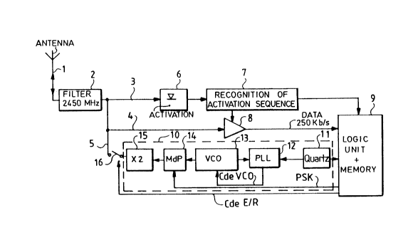
The label shown in Figure 1 has a low-gain
omnidirectional transmission-reception antenna
.o coupled to an antenna filter 2 providing sufficient
filtering so that a jammer does not desensitize the
badge in activation or writing mode.
The output of the filter 2 is coupled
respectively to an activation circuitry 3, a writing
circuitry 4 and a transmission circuitry 5.
2142498
~,
The activation circuitry 3 has amplitude-
detection means 6 coupled at output to means 7 for
the recognition and activation of the label. The
writing circuitry 4 has amplification means 8 for the
amplification of the data received by the antenna 1.
The amplification means 8 are activated by a signal
delivered by the recognition means 7. The activation
and writing means 3 and 4 are respectively coupled by
their output to a first input and a second input of
1~ digital processing means 9 comprising a logic unit
and a memory block that are known, for example a
microprocessor. The transmission circuitry 5 has a
variable oscillator-transmitter 10 demarcated by a
dashed box. The variable oscillator-transmitter 10
has a reference oscillator 11, for example a quartz
oscillator, delivering for example a frequency of
19.14 MHz. The reference oscillator 11 delivers a
clock signal firstly to the digital processing means
9 and secondly to the phase-locked loop 12 or PLL.
2!~ This look 12 has known means (not shown) formed by a
phase comparator, a frequency divider circuit, a
filter and an amplifier. The variable oscillator-
transmitter 10 also has a VCO (voltage controlled
oscillator) 13. The VCO 13 delivers a frequency,
~5 equal in this example to 1225 MHz, on a second input
of the PLL 12 and on a first input of the phase
modulation means MdP 14. The VCO 13 receives a
command, Cde CVO, at its input, delivered at output
of the PLL 12. The phase-modulation means MdP 14
receive, at a second input, a PSK (phase-shift
keying) type of modulation signal delivered by its
digital processing means 9. The output of the phase
modulation means MdP 14 is coupled to the input of
frequency doubler means 15. The output of these
.s means 15, corresponding also to the output of the
oscillator-emitter 10, is coupled to a first input of
2142498
,-
an antenna relay 16. This relay 16 is activated by a
transmission-reception command, Cde E/R, delivered by
the digital processing means 9. At transmission, the
activation and writing means 3 and 4 are inhibited
whereas in reception it is the tr~n~m;~sion circuitry
that is inhibited.
The servo-control of the frequency of the
oscillator-transmitter 10 is similar to that of a
known type of phase loop.
ii) The frequency delivered by the VCO 13 which, in
the example, is equal to 1225 MHz, is divided by 64
before being compared in phase with a frequency of
19.14 MHz coming from the reference quartz oscillator
11. The electrical signal delivered by the phase
comparator represents the phase difference between
the frequency of 1225 MHz divided by 64 and the
frequency of 19.14 MHz of the quartz oscillator 11.
The signal is then amplified and filtered by the
filtering circuit and then applied to the input
2ij called the frequency control input of the VCO 13.
The filtering circuit of the PLL 12 carries out a
servo-control of the transmission frequency on a
determined wideband so as to make the VCO 13
insensitive to the disturbances that are external and
~5 internal to the system according to the invention.
Indeed, the antenna 1 may be masked by metal objects
that mismatch it. It may also pick up powerful
radioelectrical rays which may or may not be
deliberately sent. The VCO 13 must therefore be very
swift in phase-locking.
The phase modulation means MdP 14 are formed, for
example, by a linear phase shifter circuit inserted
between the VCO 13 and the frequency doubler 15. The
phase excursion at this level is therefore equal to
half O and ~/2 for the frequency doubler 15 doubles
the modulation index; the phase modulation means MdP
`` ` 21~2~98
-
14 are formed, for example, by capacitors, varicap
diodes and inductors. The PSK modulation data coming
from the digital processing means 9, filtered in
baseband mode, control the varicap diodes. The
spectrum transmitted is thus limited in terms of
spectral occupancy.
In transmission mode, all the circuits of the
oscillator are supplied and the signal delivered by
the oscillator-transmitter 10 is sent to the antenna
Figure 2 shows a functional diagram of a portable
reader according to the invention.
This reader has a logic unit 17, for example a
microprocessor, enabling the management of the
information elements sent and received by the reader.
This reader also has a frequency synthesizer 18
generating a first frequency, for example a frequency
of 2450 MHz, and a second frequency, for example a
frequency of 2380 MHz. The difference between these
?o two frequencies constitutes an intermediate frequency
FI therefore equal to 70 MHz in this example. The
synthesizer 18 receives, at its input, a command Cde
E/R from the logic unit 17 enabling the selection of
the frequency to be delivered by the synthesizer 18.
'5 The reader then has a transmitter 19 that is
variable in amplitude, transmitting a signal at the
frequency 2450 MHz generated by the synthesizer 18.
The transmitter 19 receives a command with reduced
power, Cde PR, at a first input, the
~o transmission/reception command Cde E/R at a second
input and the two-phase data to be transmitted at a
third input. These three commands are generated by
the logic unit 17.
The reader has a receiver/phase demodulator 20
,5 demodulating the signal received at a first input at
21~2q98
the frequency of 2380 MHz, corresponding to the
second frequency generated by the synthesizer 18.
The receiver 20 receives, at a second input, a
reception command Cde R generated by the logic unit
17. At a first output, it delivers the demodulated
two-phase data elements received and at a second
output, it delivers the information on the amplitude
of the detected field. These two information
elements are injected respectively into a first input
and a second input of the logic unit 17.
An antenna 21, used both for transmission and
reception, is coupled to an antenna filter 22
centered on the 2450 MHz frequency in the example
processed, itself coupled to a switching means 23, a
relay for example, controlled by the command Cde E/R.
This command enables the selection of either the
output of the transmitter 19 or the input of the
receiver 20.
The working of the reader is as follows:
In the mode of interrogation or search for labels
to be identified, the transmitter 19 briefly
transmits, in amplitude modulation, activation
messages comprising a particular activation sequence
followed by the identity of the reader. Then the
transmitter 19 is switched over into resting mode by
the command Cde E/R and the receiver 20 is activated
pending one or more responses coming from one or more
activation labels, hence labels within
radioelectrical range. The receiver 20 demodulates
!O the phase-modulated data elements transmitted by the
labels. These data elements are transmitted to the
logic unit 17 which interprets them. This logic unit
17 then alternately activates the transmitter 19 and
the receiver 20 to transmit and receive the data
,5 elements. The reception periods are far longer than
the transmission periods. This enables the reader to
` ` 2142498
have great operating autonomy with rechargeable
batteries having a capacity of 1 ampere/hour enabling
it to be portable. The transmitted power is about
200 milliwatts and is compatible with health
S standards (< 10 milliwatts/1 cm2 at a distance of 1
cm from the antenna 21 of the reader). The receiver
is of the superheterodyne type with an
intermediate frequency FI of 70 MHz. Consequently,
when the receiver 20 is in operation, the frequency
lii of the synthesizer 18 is equal to the tr~nsm;~sion
frequency minus the value of the intermediate
frequency, giving 2380 MHz. The received spectrum is
wide, in the range of +/- 500 KHz, owing to the high
bit rate of the data elements and of the two-phase
1' FMO encoding used and the precision of the frequency
transmitted by the labels is in the range of +/- 250
KHz. The selectivity of the receiver 20 is done in
intermediate frequency FI, for example by the use of
a surface wave filter having a passband in the range
2v of +/- 2 MHz. The sensitivity of the receiver 20 is
then - 90 dBm for a bit error rate (BER) of the order
of 10-6.
To prevent jamming or interference between
neighboring readers, it is possible to change the
2~ transmission frequency by programming the frequency
of the synthesizer 18, the reception frequencies
being always the same.
The low-gain omnidirectional antenna 21 (1 to 2
dBi) can be replaced by a directional antenna with
,l~ higher gain to increase the range of the reader.
A reduced power command, Cde PR, reduces the
power transmitted so as to reduce the range of
interrogation should the carrier of the reader seek
to identify a particular label, for example a label
,~ borne by a vehicle.
2142498
-
A protocol for the exchange of information
between a label and at least one reader according to
the invention is illustrated in Figure 23 and also
enables an explanation of the working of the label
and of the reader during such an exchange.
When there is no reader in radioelectrical range,
only the activation means 6 and 7 of the label are
supplied by a battery (not shown) whose consumption
is below 5 microamperes, thus giving the label
autonomy of over 5 years. None of the other circuits
is supplied.
When a reader is within range, it sends out a
brief amplitude-modulated microwave signal modulated
by a OOK or ASK type "all or nothing" operation by an
activation sequence followed by data elements
identifying the reader. The activation means 6 of
the label then detect this message and turn on the
activation sequence recognition means 7. If this
activation sequence is truly recognized, then all the
2ij other circuits of the label are supplied. The
writing circuitry 4 amplifies the data elements sent
by the reader which are then processed by the digital
processing means 9.
It then carries out a series of information
~5 exchanges between the label and the reader in
accordance with the protocol used. This protocol has
a first stage for the identification of the label by
the transmission of data elements to the reader in
the time intervals randomly chosen from a determined
,~} number of possible time intervals, a reservation
stage where the reader orders the different activated
labels to transmit their data elements also within
well-determined time intervals, a stage for the
transmission of the data elements contained in the
.5 label to the reader, a stage for the acknowledgment
of the reader, a stage for the repetition of
2142498
-
11
exchanges in the event of failure, namely in the
event of a collision of messages and a stage for
repositioning the label in watching mode.
Among the stages of downline transmission, namely
s transmission from the reader to the label, the reader
transmits in amplitude modulation mode and the labels
are in demodulation mode in using the writing
circuitry 4 and the digital processing means 9 to
process the signal received by the antenna 1.
r, During the upline transmission stages, namely
transmission from the label to the reader, the reader
no longer transmits. The label activates its
oscillator-transmitter 10 by phase modulating it
according to two states 0 or ~ at the rate of the
data elements to be transmitted, in the range of 250
Kbits/s. Indeed, the phase modulation is chosen in
the label-to-reader direction as it is more efficient
than the amplitude modulation and can be easily
achieved in a very small-sized object such as a
70 credit card for example that costs little.
The power sent out by the oscillator-emitter 10
is low but sufficient to be undisturbed by the
radioelectrical noise sent out, for example by the
label-bearing vehicle. The range thus depends only
~s on the activation threshold. The consumption of the
oscillator-transmitter 10 is very low, lower than 10
milliamperes, and lasts only some milliseconds
necessary to transmit the data elements to the
reader.
Consequently, the reader awaiting a response from
the label or labels does not need to continuously
transmit a wave as necessary for reflective passive
labels. This prevents cluttering the RF space and
possibly jamming other neighboring readers.
Furthermore, the reader needs only one antenna 21 for
the transmission/reception unlike certain existing
```- 21~2~98
.
12
systems that require two distinct antennas, one for
transmission and one for reception.
The electrical characteristics of the reader are
considerably simplified and very easy to achieve.
The range is thus well controlled and depends only on
the downline reader-to-label path by the transmission
of a short message to activate the object to be
identified by the reader.
Figure 4 illustrates a second embodiment of a
1~ label in an identification system according to the
invention. The elements similar to those of Figure 1
are designated by the same references. In this
embodiment, the architecture of the oscillator-
transmitter 10 is modified by the use of an ASIC
(applications specific integrated circuit) 24
demarcated by a box of dashes. The oscillator-
transmitter 10, in this second embodiment, has a VCO
25 tuned directly to the frequency to be transmitted
equal, in the example, to 2450 MHz, a PLL 26
2~ including a circuitry of dividers by N, a
comparator/phase demodulator as well as a filtering
circuit not shown.
The use of an ASIC enables the optimizing of the
current consumption which thus goes below 5
~5 milliamperes in active phase. The ASIC 24 also
brings together the detection means 6 of the
activation circuitry 3 and further comprises
automatic testing means 27 that can be used to test
the efficient working of the label. This test, which
3~ simulates the reception of the data sent by a reader
in radioelectrical range, can be done regularly, it
being known that the label is essentially in a
permanent watching state, hence without disturbing
the operation of the system in the event of exchanges
~5 between the label and a reader. The test consists in
reinjecting a fraction of the microwave signal
``. 2142498
~,_
13
delivered by the VCO 25, at the 2450 MHz frequency,
amplitude-modulated by the testing means themselves,
into the input of the activation means 6. These
testing means 27 receive, at a first input, a test
command generated by the digital processing means 9.
At a second input, they receive the signal delivered
by the VCO 25. At a first input, the VCO 25 receives
the control signal, Cde VCO, delivered by a PLL 26
and furthermore receives, at a second input, a power
control, Cde P, generated by the digital processing
means 9 enabling the adjustment of the level of the
input power of the VCO 12. The PSK modulation
command is delivered by the digital processing means
9 and is injected directly into a third input of the
PLO 26, the first and the second input respectively
receiving the signal delivered by the quartz
oscillator 11 and the signal delivered by the VCO 25.
Since the other elements of the label are similar to
those of Figure 1, they are not described again.
Other alternative embodiments are possible
without in any way departing from the scope of the
invention. The transmission frequency may be
different from the reception frequency and the
adjustment of the emitted power may be programmed on
2c the basis of the data el-ements transmitted by the
reader which will have measured the field received in
its receiver and will have decided that the power
transmitted by the label is too high or too low.
This makes it possible to avoid cluttering the RF
0 space. Furthermore, the bit rate of the information
elements transmitted may be increased to over 1 Mbit.