Note: Descriptions are shown in the official language in which they were submitted.
`~o 94/10722Pcr/uss3/0859
21~2703
ELECTRICAL CONNECTOR
.' :
Back~roun~l of the lavention
5This invention relates to electrical connectors and especially
to connectors for formlng solder connections between elongate
electrical conductors.
. ~ .
Electricat connectors which contain solder inserts are widely
o used for formlng solder connectlons between elongate electrical
conductors. Such connectors are descrlbed ln US Patent Nos.
3243211, 4282396 and 4283596 and International Patent
Appltcation Pubttcatton No. WO91/11831, the dlsclosures of which
are lncorporated hereln by reference. Such electrical cormectors
5 are satisfactory for most appttcaffons, b,ut ln some sltuations they
suffer from the drawback that It ls normally posslb!e for the elongate
conductors (e.g. wlres) to sllp out of the connector prlor to the
formation of the solder connectlon.
~oln the manufacture of automottve harnesses, for e~ample, lt ls `-
usual to assemble the harness and form temporary connections
betwcen the wlres and cables so that an dectrtcat current or slgnal
may be passied through the asisembly In order to verlfy that the
harncss has been assembled correctly. It Is only after such
2s verlftcatton is obtalned that permanent electrtcal connections are
formed. The electrlcal connectors mentloned above are often
un~ for such an appltcatton, because they generalty cannot
be used to form tempora~y ~otnts whtch are dependable so that the
harness can be tested prlor to formatton of the permanent solder
30 Joint. ~ ~
~ .
The electr~cat connectors described tn Internattonal Patent
Appllcation No. WO92/00616 overcome the above drawbacks.
These devices contatn a metaltlc connect1ng element, made from
9s copper for example, havlng a taperlng intemal surface whlch has a
screw thread, so that a temporary dectrical connection between a ~ ~
~ ~ bundle of wires can be formed by scre~ng them into the connecting ~ -
;~ - element. They also contain a solder insert for forming a permancnt
connection between the wires, so that, for example, once an
`WO 94/10722 2 1 ~ 2 7 o 3 Pcr/Us93/08597
automotive harness has been tested using temporary connections,
these connections can be made permanent stmply by heating the
connectors so as to melt the solder and form solder connections.
Whllst these connectors perform cellently they have the drawback
5 that because the solder ~olnt ~s formed lnslde the connecting
element it is dimcult to inspect. In addltion, ln comparison to a
connection formed entlrely by solder, the presence of the
connecting element normally raises the welght of the connection
and also its size, for example due to the protrusion of a
o clrcumferentially extending ridge in the area of the connect~on.
.Summarv of the Invention
According to a first aspect of the invent~on, there is provided a
device for forming an electrical connection between a plurality of
elongate electrical conductors, which comprlses an electrically
insulating sleeve and a hollow connecting deinent contained within
the sleeve, the connecting dement formed from solder for forming a
solder connection between the conductors and havlng a tapering
20 internal surface that is provided wlth a screw thread, arranged so
that a temporary electrical connection between the conductors may
be formed by twisttng them into the connecting element.
Accordlng to a second aspect of the invention there is
2s provided a device for forming an electrical connection between a
pluraltty of elongate electrical conductors which comprises an
electrically insulating sleeve and a hollow connecting element
contatned wlthin the sleeve, the connecting element comprising a
taperlng coll of solder wlre for forming a solder connectton between
30 the conductors, the solder wlre havlng at least one ridge extending
hclically along at least part of its length, arranged so that a
temporary electrlcal connection between the conductors may be
formed by twisting them into the coil.
3s - According to a third aspect of the invention, there is provided
a method of forming an electrical connection between a plurality of
dongate dectrical conductors b~r means of a device accord~ng to the
inventlon, which comprises:
-
! . . 'W~ -"~- . :,, . ' .' ' ' '
~`~!Vo 94/10722 Pcr~uss3/o8ss7
-3- 21~2703
(a) twisting the elongate electrical conductors into the solder
connecting element of the device, thereby forming a
temporary electrical connection between the conductors:
s (b) heating the device so that at least some of the solder of the
connecting element melts; and ;
(c) allowlng the device to cool so that the molten solder solidifies
and forms a solder connection between the conductors. ~;
10 . ' ' ' ~
The method may additionally include passing an electrical
current through the temporary electrical connection prior to
heat~ng the device, for example in order to verl~r the connect~on
The invention has a number of advantages. Devices according
to the invention are normaUy lighter than similar devices which
contain both a connecting element that is not formed from solder ~ ~-and a solder insert, whlle 8tlll aUowing verification of the connection
before heating for example. Tnis can be sigr~ficant for applications
20 where weight mlinimtsation is important, such as in aircrait for
example. As weU as normaUy being lighter than such devices,
devlces according to the invention are often capable of form~ng less
bully electrlcal connections, since once the solder has melted the
or4~1nal connectlng element has 'disappeared' and has been replaced -
25 by a simple solder connection. In addltion, in embodiments of the
invention in which at least part of the insulating sleeve is
transparent the quality of the finished solder connection may
nonnally be inspected. This is in contrast to most connector
devices whlch contain a solder insert located inside a connecting
30 element.
., :
~vo 94/10722 2 1 4 2 7 o 3 Pcr/US93/08597
Brlef Descr~Dtion of the l:)ra~lnes
Figure 1 ls a sectional elevation along the axis of a dev~ce
according to the present invention;
Figure 2 is a sectional elevation along the a~ds of a second form
of device accordlng to the present imention:
o Figure 3 is a sectional elevation along ~e axis of a third form of
devlce according to the lnvent10n;
Figure 4 is a sectional elevation along the axis of a fourth form
of device according to the invention;
Figure 5 is a secffonal elevation along the axis of a temporary
: electrical connection between a plurality of stranded
wires which has been formed by twist1ng the wires into
the device shown in f~gure 3; and
Flgure 6 ls a sectional elevation ~long the a~Ci8 of a solder
connection between the wires, ~vhich has been forn ed
by heating the temporary connection shown in flgure 5.
.
,, .
- .:
.
. ~ . - ~- .
. ,.~.. ~ ~.
: . . ., - . . ,
~vo 94/10722 Pcr/us93/o8s97
- -5- 2~2703
Detailed Descrl~tion of the Inve~tion
The devlces according to the invention include an electrically
lnsulatlng sleeve. Usually the sleeve will be dimensionally
5 recoverable, and especially dimensionally heat-recoverable, that is to
say an article which has a dimensional configuration which may be
made substant1ally to change when sub,~ected to heat treatment.
Usually, such art~cles recover, on heattng, towards an origlnal shape
from which they have previously been deformed, but the term heat-
0 recoverable, as used herein, also includes articles which, on heating,adopt a new configuration, even if they have not previously been
deformed.
The heat-recoverable sleeve may comprise a heat shrinkable
15 article made from a polymeric-materlal exhibit1ng the property of
elasttc or plastlc memory as described, for example, in US Patents
2,027,962; 3,086,242 and 3,597,372. As is made clear in, for
example US Patent 2,027,962, the orlginal dimensionally heat-stable
form may be a translent form in a conttnuous process in which, for
20 example, an extruded tube is expanded, whllst hot, to a
dimenslonally hcat-unstable form, but, in other appllcations, a
preformed dlmenslonally heat-stable article ls deformed to a
dimensionall~ heat-unstable form in a separate state.
Any materlal to whlch the property of dimensional
recoverability may be imparted may be used to form the sleeve.
Preferred materials lnclude: low, medium or high denslty
polyethylene: ethylene copo~mers, e.g. wlth alpha oleflns such as l-
butene or l-hexene, or v~nyl acetate; polyamides, especially Nylon
materlals, e.g. Nylon 6, Nylon 6.6, Nylon 11 or Nylon 12: and
fluoropolymers, e.g. polytetrafluoroethylene, polvinylidenefluortde.
ethyl'enetetrafluoroethylene copolymer or vinylldenefluortde
tetra~uroethylene copolymer.
As mentioned above, according to a flrst aspect of the
inventton the connecttng element of the device has a tapering
internal surface that is provided with a screw thread, arranged so
that a temporary electrical connection between a plurality of
elongate electrical conductors may be formed by twisting them into
-
~0 94/10722 Pcr/US93/08597
- -6- 2142703
the connecting element. The connecting element may, for example,
be formed from a hollow solder preform, preferably having a
substantially conical or frusto-conlcal Interior. More preferably the
solder preform ltself has a substantlally conical or frusto-conical
5 shape. The screw thread may be formed In any one of a number of
conventlonal ways, but preferably lt 1s formed by stamping.
According to certain preferred embodiments of the invention,
the connectlng element of the device Is formed from a taperlng coil
lO of solder ~re. The solder wlre may generally have any cross-section
whlch will allow a temporary electrical connectlon to be formed
between a plurality of elongate electrical conductors by twisting
them Into the taperlng coil. Preferably, however, the cross-section
of at least part of the wlre is such that the wlre has at least one rldge
lS extendlng along at least part of ~Its length. More preferably at least
part of the solder wire has a substantially polygonal, especially
rhombic, cross-section, and the angular portions of the cross-section
may form ridges extending along at least part of the length of the
wire.
When the connect~ng element accordlng to the first aspect of
the invention is formed from a tapering coil of solder wire, the
screw thread of the connect~ng element is preferably formed from at
least one ridge extending along at least part of the length.
2s
As already mentioned, a temporary electrical connection
between a plurality of elongate electrical conductors may be formed
by twisiting them into the connecting element of a device according
to the first asipect of the invention. It ls possible that the action of
30 twisting the conductors into the taperlng internal siurface of the
connecting dement normally causes the conductors to twist about
themselves to a degree. Subsequent accidental removal of the
conductors is normally inhibited, possible because the twisted
conductors are caught within various parts of the screw thread. It
3s has been found that particularly reliable tempora~y connections may
often be formed when stranded conductors are used, presumably
because the strands themsehres may be twisted and may therefore be
caught within parts of the screw thread.
, - --, .: -~
-`;vo 94/10722 2 1 ~ 2 7 o 3 Pcr/US93/08597
-7-
ln a particularly preferred embodlment of the device
accordlng to the flrst aspect of the invention, the screw thread of
the connecting element is perlodically interrupted along at least
part of its length. These interruptions may, for example. take the
s form of indentations, and preferably substantiaUy ~ or 'U' shaped or
. rectangular indentations in the teeth of the screw thread. Where
the connecting element 18 formed from a coil of solder wire, the
wire may be provided with a number of interruptions whlch also
prefcrably take the form of lndentatlons whlch preferably
o substantlaUy ~ or 'U' shaped or rectangular when viewed from the
side of the wire. The grooves may be located next to one another so
that they 'touch' or they may be separated from one another to a
greater or lesser extent. Where the connect~ng element ls formed
from a horiow solder preform the lnterrupted screw thread may. for
s example, be formed by stamping and where lt is formed from a coil
of solder wire the interrupttons may, for example, be formed in the
wlre by means of a toothed roller.
Provlding the screw thread of the connecting dement with
20 periodtc interrupttons along at least part of lts length may often
improve the reliabiltty of temporary dectrical connect~ons formed by
means of the device. It is possible that this ls because the degree to
which the conductors are twlsted about themselves is increased
slnce the conductors become caught ln the interrupttons in the
2s screw thread when they are twtsted into the cormecting dement.
As mentioned above. the hollow connecttng dement of the
device accordLng to the second aspect of the invention comprises a
tapering coll of solder wire, the wlre having at least one rtdge
30 extending heltcally along at leasit part of lts length, a~anged so that a
temporary dectrtcal connectton between a pluraltty of elongate
electrtcal conductors may be formed by twtstlng them lnto the coll.
The solder wlre accordlng to thts aspect of the inventton may be
formed ln a number of different ways. For example, thé wlre may be
35 drawn in order to form lt into the required thtckness and also in
order to provide lt with at least one rtdge extendtng along at least
part of lts length, and subsequent to thts the drawn wlre may be
twisited in order to cause the or each rtdge to extend helically.
Alternatively for example, the or each rtdge tn the w~re may be
,,~
~ - \
io 94/10722 2 1 ~ 2 7 o 3 PCI~/US93/08597
caused to extend hellcally at the same tlme as the wire is drawn.
either by twisting the wire as lt passes through the draw plate or by
rotating the draw plate ltsdf.
It ~s belleved that the connectlng element of the device
accordlng to the second aspect of the lnvention may provlde
temporary electrlcal connectlons in a æimilar way to that of the
device accordlng to the flrst aspect of the invention wherein the
screw thread ls periodlcally lnterrupted along lts lcngth. It is
0 possible that the helically extending ridge(s) of the solder wtre may
act as periodlc protruslons on the tnside of the w~re coil whlch may
increase the degree of twlstlng of the elongate electrical conductors
about themsehes when they are twisted into the coil. Subsequent
accldental removal of the conductors ls nonnally inhiblted possibly
because the twisted conductors~are caught between the protrusions
and/or the wlndlngs of the wlre coil.
The connecting element of the device according to the second
aspect of the lnvention may be formed so that the coil of the solder
20 wlre and the helbc or helices of the or each ridge extending along at
least part of the length of the wire have the same or opposlte
handedness.
The devices according to the flrst and second pects of the
2s ~nventlon include, rcspectivel~r: a hollow solder connect~ng element
havlng a taperlng intemal surface provided with a screw thread; and
a hollow connect1ng element comprislng a tapering coil. Each of
the~e devices may be u~ed to form a stub splice between a pluraltty
of elongate electrical conductors lnserted lnto one end of the
30 lnsulating sleeve. the other end of the sleeve for example being
closed,~especially be means of a sealing ball as described ln
International Patent Applicatlon No. WO91/1 18Sl, the dtsclosure of
which ls incorporated herein by reference. Alternattvely, however,
the internal surface of the connect1ng dement or the coll of solder
3s wlre respecttvely may taper in two opposlte directtons to an
intermedhte regton of minimum dlameter, for example in a 'diabolo'
shape. These forms of device may therefore be used to form in-line
spltces between a plurality of elongate dectr~cal conductors. Other
forms of device according to the inventton may also achieve this
~, ., .... , ,.,,, ,. ,. , . . ~.. - . ~ .. ,
``10 94/10722 PCI~/US93/08597
9 2142703
purpose; according to these embodlments of the invention the
device may include respectively a second solder connecting
element having a tapering internal surface that ls provlded u~th a
screw thread connected to the flrst connecting element by
5 connecting means; or a second connecting dement comprlsing a
second tapering coll of solder wire connected to the first coil of
solder wire by connecttng means. me conneetlng means may take
any appropriate form, for example lt may comprlse a substantially
eyllndrleal element that ls provided wlth two or more protrusions or
o grooves wh1eh are eapable of interloeklng with the two eonnect~ng
eléments. It Is posslble for the two conneet1ng elements to be
rotatable with respect to each other and/or for the two coils or -
sere v threads respeetivel~r to have the same or opposlte handedness
.~
The solder of the connectlng element of the devices accordlng
to the Inventlon may comprlse any one or more approprlate solder
eompos1ttons. For example, lt may be formed from an Sn63 Pb37 or
an Sng6.s Ag3.s eutecttc eomposlt~on. In embodlments of the
~nverit~on where the eonneet1ng element eomprlses a hollow solder
20 preform, the preform may for example eomprlse a eomposlte havlng
a portlon that ls formed from a rdat~vely hlgh mdttng polnt solder
and a port~on that ls formed from a rdatlvdy low melt1ng polnt
solder, as deserlbed In Internat~onal Publteat~on No. W088/09068
In this form of devlee, melt~ng of the hlgher melt~ng point
25 eomponent e.g Sng6.5 Aggi.s eutectie wLU normally provide a vlsual
Indleatlon that the devlee has been heated suffle~ently to melt the
lower melt~ng potnt component and to form a satlsfactory solder
plnt. If deslred, the lo~ver melttng polnt eomponent may be of non-
euteet~c eompos~tton and, for example as desertbed In Internattonal
30 Publieation No. WO90/09255, the higher and lower melt1ng point
compon~ents may together form a eutectlc composltion. For
example, a non-eutectie Sn60 Pb40 lo~ver meltlng polnt component
may be employed with a higher melt1ng polnt eomponent formed
from pure ttn in relative amounts sueh that an Sn63i Pb3i7 eutectic is
35 formed. The dlselosures of these two patent appllcations are
incorporated herein by referenee. An advantage of emplaying a two
component solder, and especiaUy a ttn, Sn60 Pb40 combtnation is
that lt reduces the poss~b~ty of 'wicking', that is to say, travel of
`: :
~o 94/10722 Pcr/us93/o8s97
- -lO- 2142703
solder away from the Jolnt area due to c~plllary act10n, which can be
caused by prolonged heattng of the device.
The solder connectlng element of the devlce accordlng to the
5 lnventton may advantageously be provlded wlth a core of flux. In
embodlments of the lnvention where the connecting element
comprtses a tapering coil of solder wlre, lt ls particularly preferred
that at least part of the solder wire ls hollow along lts length and
contalns a quantlty of flux.
In preferred embodlments of the inventlon, the sleeve of the
de~ices conta~ns a quantlty of fus~ble polymerlc material. The fuslble
polymeric material may, for example, be present ln order to seal an
electrical connectton formed by means of the device from molsture
lS lngress and/or lt may be present tn order to provide strain reltef to
the connectton. The materlal may be present tn the form of at least
one Insert havlng any one of a vartety of shapes, such as for example
a baU, a peUet or a rtng.
The fusible polymeric material according to the lnventton
preferably comprlses a thermoplastic materlal, for example a hot~
melt adhes~ve. The materlal may, for example, be formed from an
olcftn homopolymer or from a copolymer of an olefln wtth other
oleflns or ethylentcaUy unsaturated monomers. Preferred examples
2s lnclude high, medlum or low denslty polyethylene or ethylene
copo~mers with alpha oleflns; especiaUy C3 to C8 alpha oleflns, vinyl
acd~ or ethyl acrylate. ~lternatlvely, the materlal may be formed
from polyamtdes, polyesters, halogenated polymers and the like
Preferred polyamtdes include those havtng an average of at least 15
; i 30 carbon atoms between amtdé llnkages, for example those based on
dimer ac~ds andlor dtmer dlam~nes. E~camples of such adheslves are
gtven in US Patents Nos. 4018733 to Lopez et al and 4181775 to
Corke, the dlsclosures of whlch are incorporated herein by
reference.
3s ' ~:- ~ -
Four forms of devtce according to the tnvention wlll now be
descrtbed by way of example with reference to the accompanying
drawings.
` ~0 94/10722 2 1 gL 2 7 o 3 PCr/US93/08597
Figure 1 shows a device 1 for forming an electrical connection
between a plurality of elongate electrical conductors, whlch
comprises an electrically insulating sleeve 2 containing a hollow
connecting element 3 formed from solder, whlch has a tapering
s internal surface that is provided with a screw thread 5, a fing of
fuslble polymerlc material 7 located lnslde the sleeve beyond a
relatively wlde open end 9 of the connect1ng element and a seallng
ball ll located inslde the sleeve beyond a relatively narrow end 13 of
the connecting element, the sealing ball seallng one end of the
o sleeve.
:
The connecting element 3, whlch ls for formlng a solder
connectlon between the elongate conductors, comprises a hollow
substantially frusto-conlcal preform of Sn6s PbS7 eutectic alloy. The
5 insulating sleeve 2, which ls for~ed from crosslinked and exI)anded
polyvinylidene fluoride, ls dimenslonally heat-recoverable and has an
open end 14. The sealing ball l l is formed from lrradiated or non-
irradiated poyethylene, and the ring of fuslble polymeric matefial 7
is formed irom a polyamide composition.
Figures 2, 3 and 4 each show a further form of device
according to the invention. These devices are sim11ar to that shown
in flgure l, the only difference in each being the type of connecting
dement used.
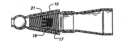
In figure 2, the connecting element 15 is Identical to the
connect1ng element 3 of Figure 2 with the exception that Its screw
thread Is periodicaUy interrupted along at least part of its length by
~ shaped indentations l9 and 21. Only a few of the indentations l9
30 and 21 are shown in the drawlng. The indentations indlcated l9 are
shown in order to illustrate indentations which are 'touching' and
those indicated 21 to illustrate indentations which are separated
from one another.
The connecting element 23 shown in flgure 3 comprises a
tapering coil of substantially square cross-section solder wlre. The
screw thread 25 of the connecting element is formed from a rid8e
27 extending along the length of the wire, the ridge itself
., .
r~
S;~
.
io 94/10722 2 1 ~ 2 7 ~ 3 Pcr/us93/o8s97
-12-
comprising an inwardly-directed angular portion of the square cross-
section wire.
The connectlng element 29 of the device shown ln figure 4
5 also comprlses a taperlng coll of substantlally square cross-section
solder wlre. However, in thls devlce the square cross-sect~on solder
~re ls twlsted so that lt has four rldges 31, correspondlng to the
four rlght angles of lts cross-sectlon, extendlng hellcally along its
length.
Flgures 5 and 6111ustrate the method of fonnlng an electrical
connectlon accordlng to the inventlon. Flgure S shows the devlce of
.
flgure 3 and a plurallty of stranded lnsulated electrlcal wlres 33; a
length of lnsulatlon has been strtpped from one end of each wlre and
these ends of the wlres have been lnserted lnto the open end 14 of
the heat-recoverable sleeve 2 and twtsted lnto the connecting
dement 23 through lts rdatlvely wlde open end 28, thereby forming
a temporary electrtcal connectlon between the wlres.
. ,
Ftgure 6 shows a solder connectton 35 between the w~lres 33
of flgure 5 whtch has been formed by heatlng the devlce of flgure 3 -
subsequent to the formatlon of the temporary electrtcal connection
between the wlres. Heat~ng the devlce has caused the solder
connect1ng element 23 to melt, the sleeve 2 to recover about the
wlres 33 and the fuslble polymertc materlal 7 to fuse between the
wtres and the sleeve. The solder whlch has mdted and then
soltdlfted Is tndlcated 37.
-. . . ~ .
: ,; :~, ~
-