Note: Descriptions are shown in the official language in which they were submitted.
214~776
CONTRQr T ~P~r ~ VIS~ PO1nR SIJPP~Y
FIELD OF THE INVENTION
The present invention relates generally to
controllable inverter power supplies and, in particular to a
method and apparatus for providing a stabilized arc when
GTAW welding.
BACKGROUND OF THE I-N V ~:N 11ON
Gas tungsten arc welding (GTAW), also called
tungsten inert gas (TIG) welding, is a well known method for
welding metals, in particular aluminum and magnesium. A
description of GTAW, including the problems associated with
welding aluminum and magnesium, may be found in Weldinq
Handbook Chapter 3, Gas Tungsten Arc Welding, pages 74-107,
1991, published by the American Welding Society.
It is well known in GTAW to use an ac squarewave
power source, which is particularly suited for welding
aluminum and magnesium. An ac squarewave power source
provides a single phase output having a straight polarity
(electrode negative) half-cycle and reverse polarity
2142776
(electrode positive) half-cycle, with a rapid transition
between half cycles.
In GTAW welding a squarewave having independently
adjustable duration of the two half-cycles (positive and
negative) is desirable. In other words, it is desirable to
have the positive half cycle duration be controllable to be
longer or shorter in time than the negative half-cycle.
Hereinafter independent control of the positive and negative
half-cycle widths is called adjustable balance. It i8 also
desirable to independently control the amplitude of the two
half-cycles, i.e. control the positive half-cycle amplitude
to be greater or less than the negative half-cycle amplitude
(hereinafter independent amplitude control).
One ac squarewave power source is described in
U.S. Patent No. 4,038,515, (the '515 patent) issued July 26,
1977 to Robert L. Risberg. The device disclosed in the '515
patent uses a single phase input and provides an ac
squarewave welding current output, with adjustable balance,
i.e. the duration of the electrode positive and electrode
negative half-cycles may be adjusted with respect to one
another.
However, a power supply that uses a single phase
input such as the power supply of the '515 patent requires a
very large single phase input current requirement. Such a
large single phase current draw is undesirable for
industrial sites having three-phased power because it
unbalances the power lines.
There are prior art GTAW power supplies using an
inverter with a three phase input that have the capability
of independent control of the output half-cycles. However,
many prior art GTAW inverter power supplies directly rectify
the input line. Thus, to design inverters for multiple
21~2776
input voltages operating directly from the power lines
requires compromises in the design, such as dual inverters
with a series parallel connection, or over current and over
voltage ratings on the power components to be re-linkable
for the various inputs. Moreover, such designs provide an
input power factor that is highly capacitive. Such an input
power factor can cause neutral unbalance and line no~h~g.
Accordingly, it is desirable to provide an inverter for GTAW
that provides a constant secondary voltage, regardles~ of
the input voltage and that provides a relatively high power
factor for a welding power source.
There are additional problems with known inverter
GTAW power supplies. Inverter power supplies for GTAW
generally provide a substantially triangular wave shape load
current. Due to this triangular wave shape, in a welding
application, or any other application where wide range of
output currents is required, it can be costly to size the
output inductor to both the minimum and maximum current
required by the load, unless current discontinuities can be
accommodated.
For example, a welding power supply may be
required to go from 20 amps or less to 300 amps or more. In
order to accommodate a low current, an inductor must be very
large. It is costly to provide an inductor that will
accommodate this wide range of currents, without causing
discontinuities in the ouL~uL current. Moreover, a small
inductor is desirable for applications which require pulsing
and output because a large inductance will cause the slewing
rate of the output to be slow, adversely affecting the shape
of pulsed or squarewave outputs.
Unfortunately, the discontinuities in the output
current will appear as an arc outage which is generally not
2142776
acceptable in GTAW. Accordingly, it is desirable to provide
an inverter power supply for GTAW that is capable of
providing a wide range of output currents, yet does not
provide output current discontinuities and still does not
require the use of a costly large inductor.
When providing a GTAW inverter power supply it is
desirable to provide the user with the option of selecting
straight polarity, reverse polarity or alternating polarity
welding. Such a machine has a wider range of applications
and is more desirable to the purchaser. It is well known in
the prior art that it is difficult to start an arc when the
electrode is negative. Conversely, when the electrode is
positive the arc will start much easier. However, most dc
GTAW is done with the electrode negative, when it is
difficult to start.
Accordingly, it is desirable to provide a GTAW
inverter power supply that provides an arc starting
capability wherein the arc is started with a brief electrode
positive polarity followed by a rapid reversal to electrode
negative polarity for the welding process. Additionally,
when using ac GTAW for the reasons stated above it is
desirable to provide an extended electrode positive period
in order to facilitate arc starting.
It is also well known in the art that in ac GTAW
the arc extinguishes with every current reversal. When the
reversal is in the direction of electrode emitting (from
electrode positive to electrode negative), the arc will
reignite without much difficulty because of the thermionic
state of the electrode. However, when the reversal is to
the workpiece emitting (from electrode negative to electrode
positive), arc reignition problems are encountered. The
workpiece is generally below thermionic temperature. Also,
2i4277(j
the molten weld pool is very clean metal due to the ionic
bombardment during past electrode positive half cycles.
Both of these factors contribute to difficulty in
reestablishing the electrode positive half cycle.
One way the prior art has comr~c~ted for this
difficulty is by providing high frequency overlays.
However, there are many problems associated with such high
frequency overlays, one being that high frequency can
provide undesirable noise which adversely affects the
operation of control circuits, telecommunication equipment
and computer equipment. Accordingly, it is desirable to
provide a GTAW power supply that will provide for arc
starting (stabilizing) when trying to reestablish the
electrode positive half cycle without the use of
superimposed high frequency.
An additional problem with inverter power supplies
is that a considerable amount of acoustic noise is generated
by current reversal. Moreover, this acoustic noise is
greater for greater welding currents. Accordingly, it is
desirable to provide a GTAW power supply that will provide
for a lower output current immediately before current
reversal.
Inverter power supplies will have a distributed
(parasitic) inductance in the load (from the weld cables and
arc e.g.). This parasitic inductance will slow the
transition at current reversals, adversely affecting machine
performance. A high forcing voltage will cause a rapid
current reversal. However, a high forcing voltage may cause
damage to switches in the inverter. Thus it is desirable to
provide a forcing voltage sufficiently high to cause a
smooth and fast current reversal, but not so high as to
damage switches.
2142776
Finally, it is well known that there is an
additional safety factor with respect to ventricular
fibrillation, the major cause of ele~L~o~tion, of dc when
compared to ac. This factor is given in IEC 479 as 3.75.
Accordingly, it is desirable to provide a GTAW power supply
that provides a dc voltage at the terminals when not welding
or when the power source is at open circuit.
SUMMARY OF THE P~ENT INVENTTON
According to one aspect of the present invention a
power supply for providing an ac output to a load is
provided. The power supply includes a first source of dc
power and an inverter that receives the dc power and
provides an ac output to the load. A second source of dc
power is provided with at least one controllable switch that
connects the first and second sources of dc power in ~erie~
with the load. In one embodiment the power sources are
connected in series with every output current reversal.
According to a second aspect of the invention a
power supply for providing an ac output to a load includes a
transformer and a rectifier connected across the
transformer. A capacitor is connected across the rectifier
to provide a substantially dc voltage. A converter is
connected across the capacitor to produce a substantially dc
current having a selectable magnitude as an output. An
invertor receives the substantially dc current and provides
an ac output to the load. A second source of dc voltage is
provided and the converter includes a switch capable of
connecting the substantially dc voltage and the second
source of dc voltage in series with the load.
A third aspect of the invention is a power supply
for providing an ac output to a load. The power supply
21~2776
--7--
includes a controllable source of dc current whose magnitude
is responsive to a current reference signal. A control
circuit provides the current reference signal, wherein the
current reference signal is pulsed immediately prior to the
ac output reversing polarity.
Yet another aspect of the invention is a buck
converter comprised of a source of dc voltage provided
between first and second buses. At least one switch having
a control input is connected to the first bus and a current
gate is connected between the switch and the second bus. At
least one inductor is connected at one end to the node
common to the switch and the current gate, and the output of
the converter is across the second bus and the other end of
the inductor. A variable frequency saw tooth wave generator
is connected to the control input, and the switch is turned
on at the frequency of the saw tooth wave. The frequency of
the wave is chosen to be inversely related to the desired
current output magnitude.
In accordance with a final aspect of the invention
an ac/dc GTAW power supply for providing an output to an arc
comprises a dc source of current and an inverter that
inverters the dc current to provide an ac ouL~u~, or a dc
output of either polarity to the arc. In the event the user
selects either an ac or dc electrode negative output a
period of electrode positive dc energy is provided at start
up to help establish the arc.
Other principal features and advantages of the
invention will become apparent to those skilled in the art
upon review of the following drawings, the detailed
description and the appended claims.
21~277~ -
BRIEF DESCRIPTION OF THE DRAWINGS
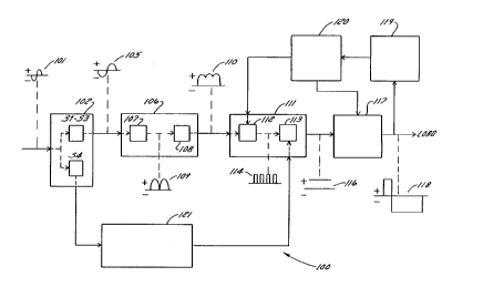
Figure 1 is a block diagram of an ac/dc power
supply constructed according to the present invention;
Figure 2 is a circuit diagram of a preferred
embodiment of the inverter power supply constructed
according to the present invention;
Figure 3A-3D depicts waveforms of the load current
and switch state of an inverter constructed according to the
present invention;
Figure 4 is a circuit diagram of a preferred
embodiment of the inverter power supply constructed
according to the present invention; and
- Figure 5 shows waveforms of the reference current
signal and the output current of the circuit of F~gure 4.
Before explaining at least one embodiment of the
invention in detail, it is to be understood that the
invention is not limited in its application to the details
of construction and the arrangement of the components set
forth in the following description or illustrated in the
drawing. The invention is capable of other embodiments or
being practiced or carried out in various ways. Also, it is
to be understood that the phraseology and terminology
employed herein is for the ~uL~ose of description and should
not be regarded as limiting.
DETAILED DESCRIPTION OF A P~EFERRED EXEMPLARY EMBODIMENT
The present invention is directed primarily ~o an
inverter power supply for use in ac or dc GTAW welding.
Referring to Figure 1, a block diagram of a preferred
embodiment of a GTAW power supply 100 is shown.
Additionally, waveforms between and within various stages of
GTAW power supply 100 are shown.
21~2776
g
As will be described in detail below, GTAW power
supply 100 provides an output suitable for ac or dc GTAW
welding. In the ac mode GTAW power supply 100 provides an
output having adjustable balance and independent amplitude
control. Moreover, even at low currents discontinuities in
the load are avoided. Also, as the current reverses from
one polarity to the other, a burst of energy is provided to
help re-establish the arc and avoid arc instability.
Similarly, in the dc electrode negative mode GTAW power
10 supply 100 provides a short burst of electrode positive
current to start the arc.
As shown on Figure 1 an input 60 Hz ac supply 101
is provided to a transformer stage 102. Transformer stage
102 includes a plurality of main secondary windings S1-53
and a clamp secondary winding S4. Input supply 101 i8 a
high voltage, low current source and is transformed to a 60
Hz ac low voltage, high current, output 105 through main
secondary windings S1-S3. Of course as one skilled in the
art will recognize the frequency may be something other than
60 Hz for both the input and the output.
~ow voltage, high current, output 105 is provided
to a rectifier stage 106 which includes a diode bridge 107
and a capacitor 108. Diode bridge 107 receives 60 Hz low
voltage, high current output 105 and rectifies it to a
rectified dc signal 109. Rectified dc signal 109 is received
by capacitor 108, which provides a filtered dc signal 110
having a magnitude of approximately 85 V. In practice
capacitor 108 may be more than one capacitor, reducing costs
and improving performance. In alternative embodiments
transformer stage 102 and rectifier stage 106 may be
replaced by other components which provide a source of dc
current.
214277~
--10--
Filtered dc signal 110 is received by a buck
converter stage 111 (also called a switching regulator)
which includes a switch 112 and an inductor 113. Switch 112
receives filtered dc signal 110 and provides a chopped dc
signal 115, preferably having a frequency in the tens of Xhz
range. As one skilled in the art should recognize, the
frequency of chopping could vary widely, depending upon the
particular application needed and the components used to
perform the switchi~g. Chopped dc signal 115 i~ provided to
inductor 113 which provides a smoothed dc signal 116 as an
output. In practice switch 112 may be implemented using a
variety of semiconductor switches, including MOSFETs, and
inductor 113 may be more than one inductor. Smoothed dc
signal 116 has a variable magnitude, depending upon the
magnitude of filtered dc signal 308 and the switch~g of
buck converter stage 111.
Smoothed dc signal 116 is provided to an inverter
stage 117, which includes IGBTs or other semiconductor
switches in the preferred embodiment. Inverter stage 117
inverts its input and provides an ac output 118, having
variable frequency, adjustable balance and independently
controlled amplitude. The frequency and width of output 118
are controlled by the switching of inverter stage 117. The
magnitude of output 118 is dependent on the magnitude of
smoothed dc signal 116, which in turn is controlled by the
switching of buck converter stage 111. When operating in
the dc mode output inverter stage 117 is controlled to
provide a constant polarity dc output.
The magnitude, duration and freguency of output
118 is sensed by a sense circuit 119. Sense circuit 119
provides that information to a control circuit 120. Control
circuit 120 provides switching signals to switch 112 to
~1~277~
control the magnitude of smoothed dc signal 116 and,
consequently, output 118. Control circuit 120 also provides
switching signals to inverter stage 117 to control the
frequency and balance of output 118.
Clamp secondary S4 is provided to help protect
stage 117. Clamp secondary S4 transforms input 101 to a 120
volt, low current signal and provides it to a clamp stage
121. The output of clamp stage 121 i8 a filtered dc signal
of about 165 volts. As will be explained in detail below
with respect to Figure 4, clamp stage 121 effectively clamps
the voltage applied to IGBTs in inverter stage 117 to a safe
level. Thus, clamp stage 121 protects IGBTs in inverter
stage 117.
Referring now to Figure 2, a circuit diagram of
one embodiment of GTAW power supply 100 is shown. The
embodiment of Figure 2 has the stages of Figure 1, except
clamp secondary S4 and clamp stage 121. Sense circuit 119
and control circuit 120 are used in the embodiment of Figure
2, but are not shown.
The circuit of Figure 2 includes transformer stage
102, rectifier stage 106, buck converter stage 111, and
inverter stage 117. Transformer stage 102 includes a
transformer Tl, which has a plurality of windings Pl-P3 and
secondary windings Sl-S3. Transformer stage 102 is designed
with some primary/secondary leakage reactance in order to
obtain a high power factor. For example, using a
primary/secondary leakage reactance in the range of 1.0-1.5
millihenrys at 230 V, a power factor of .94 is obtained.
Preferably, a power factor of at least 0.90 is obtained.
Primary windings Pl-P3 receive as an input three-
phase input signal 101 (Figure 1) on a plurality of input
terminals Vl-V3. As shown in Figure 2, a three-phase input
2142776
and three-phase transformer is utilized. However, as one
skilled in the art will readily recognize a single-phase
input and single-phase transformer could also be used.
Secondary windings S1-S3 are designed to produce
an ac output of 60 V each. GTAW power supply 100 can be
designed for any of a variety of st~Ard voltages by
providing a different primary winding depending upon the
input voltage. For example, the primary windings may be
designed to accept any voltages, such as 200, 220, 230, 380,
400, 415, 460, 480 and 575, and any frequency such as 50 or
60 Hz. Indeed, the primary could have capped windings or
extended windings such that the same transformer can
accommodate multiple input voltages.
The output of secondary windings S1-S3 is provided
to rectifier stage 106 which includes diode bridge 107 and
capacitor 108. Diode bridge 107 includes 6 diodes 207 and
capacitor 108 has, in the preferred embodiment, a large
value (24,000 mfd) and is charged to 85 V. Capacitor 108
filters the dc rectified signal to produce a filtered dc
signal of about 85 v between the positive bus and negative
bus.
The output of rectifier stage 106 (the positive
bus and negative bus) is provided as the input to the buck
converter stage 111, sometimes called a chopper. In this
embodiment buck converter stage 111 is comprised of a switch
(MOSFET) Q1, a diode D4 and an inductor L1. As one skilled
in the art will recognize other electronic components having
the ability to control current flow (a current gate) may be
used in place of MOSFET Q1 and/or diode D4.
Buck converter stage 111 performs a function
analogous to a dc transformer. In other words it receives
as an input the 85 V dc supply and provides a substantially
21~2776
dc output having a controllable adjustable magnitude.
MOSFET Q1 is switched on and off at a frequency much higher
than the line frequency. In one unique embodiment, thi~
frequency varies from 24 kHz at high current demand to 60
kHz at low current demand. The relationship between the
switching frequency of MOSFET Q1 and the output current will
be explained in greater detail below.
Generally speaking the buck regulator controls the
current by pulse with modulation (PWM). In a PWM controller
the output is a function of the ratio of on time to of~ time
at the given frequency. If this on time to off time ratio
is large, the PWM will produce high power. If it is low, it
will produce low power.
The output of buck converter stage 111 i5 provided
to inverter stage 117. Inverter stage 117 comprises a
plurality of switches Q3-Q6, and provides its o~ L to a
load 208. To understand the operation of buck converter
stage 111 it is necessary to consider the state of the
switches in inverter stage 117. For example, assume that
switches Q3 and Q6 are on, thereby providing current to load
208. When MOSFET Q1 is turned on the 85 V bus will be
switched across diode D4. Diode D4, of course, is blocking,
thus this voltage appears across switches Q3-Q6 (IGBTs in
the preferred embodiment). Because switches Q3 and Q6 are
on, positive current will flow through switch Q3, arc load
208, switch Q6 and inductor L1. If inductor L1 was not
present the current flow would be approximately equal to 85
V divided by the load impedance. In the case of an arc
load, this impedance is very low, thus the current would be
extremely high and essentially out of control.
Thus, the function of inductor L1 is to buck this
current and, while doing so, store energy. By bucking the
21~2~76
current, the current flow through load 208 is controlled and
regulated to a relatively slow rising value. Also, as the
current increases a magnetic field is induced in inductor
L1, thus storing energy therein. In other words, inductor
Ll filters pulse width modulated voltage pulses supplied by
MOSFET Ql, and provides predetermined rising and falling
current slopes to the arc through output inverter stage 117.
When Ql is switched on, the 85 V bus i~ connected
to the arc load in series through inductor Ll and output
inverter stage 117. The filtering function of Ll will cause
the output current to change at a rate equal to the forcing
voltage applied to Ll, multiplied by the on time of MOSFET
Ql, divided by the inductance value of Ll. Thus, the
current will continue to rise so long as MOSFET Ql stays on.
MOSFET Ql is turned off after a time determined by
the desired load current flow and the actual load current
flow. When MOSFET Q1 is switched off, the arc or load
current will continue to flow, but will be diverted through
free-wheeling diode D4, and again the filtering function of
L1 will cause the arc current to decrease at a rate
determined by the forcing voltage applied to Ll, multiplied
by MOSFET Q1 off time, divided by the inductance of inductor
L1. The forcing voltage applied to inductor Ll when MOSFET
Q1 is off is the arc or load voltage plus all series voltage
drops in the current path. When MOSFET Q1 is off, the
current flows from point A through diode D4, switch Q3, load
208, switch Q6, and back to inductor L1.
In summary, as long as MOSFET Q1 is on the
magnitude of the output current increases, and as long as
switch Ql is off the magnitude of the output current
decreases. Thus, by turning MOSFET Q1 on and off at regular
intervals, it is possible to regulate the load current.
21i2~76
-15-
The control of MOSFET Q1 utilizes a saw tooth
wave, a feedback signal, and a reference current signal. A
saw tooth wave signal is generated in accordance with well
known prior art, and is used to turn on MOSFET Ql at regular
intervals. Also, for any given desired output current, a
reference current signal is established. The reference
current signal is compared to a feedback signal representing
actual current to generate an error signal. MOSFET Ql is
then turned off whenever the output current reaches a
predetermined value as determined by the reference current
signal compared to the load current signal.
As one skilled in the art will recognize, this
load current will have somewhat of a triangular wave shape,
rising during the time MOSFET Q1 is on and falling during
the time MOSFET Q1 is off. The amplitude of the rise and
fall can be determined by the switching frequency of MOSFET
Q1, the on time to off time ratio of MOSFET Q1, the size of
the inductor L1, the source voltage and the load voltage.
The triangular wave shape may be seen in Figure 3,
which shows the state of MOSFET Ql and the output current
through load 208 for both high and low output currents.
Figure 3A shows the state of MOSFET Ql for a high output
current. It may be seen that switch Q1 is on for a
relatively large portion of time (approximately 75 percent
of each complete cycle). As shown in Figure 3B the
corresponding output current is relatively high and rises
during the time switch Q1 is on, and falls during the time
switch Ql is off.
Similarly, Figures 3C and 3D show the state of
switch Q1 and the output current for a low output. It may
be seen in Figure 3C that switch Q1 is off for a relatively
large portion of time (approximately 85% of the time). It
21~277~
should be noted that as shown in Figure 3 the time of one
complete cycle (on time plus off time) of switch Ql is the
same for high and low currents. In one embodiment the
switching frequency of switch Q1 will vary, depending upon
the magnitude of the output current.
As shown in Figure 3D the rise time is
sufficiently less than the fall time for such a low ou~u~
current, so the output current reaches zero prior to the
~ switching on of switch Ql, causing current discontinuities
in load 208. Such current discontinuities are common in the
prior art and are not acceptable for welding applications.
In accordance with one embodiment of the present
invention the switching frequency of switch Ql is increased
as the current decreases to prevent such current
discontinuities. The frequency is determined through
practice when considering the desired output, the inductor
size, the conduction losses in switch Q1, the switching
losses of switch Q1, losses of the snubbers that are
required for switching of switch Q1, the ripple tolerance in
load current, and other well known engineering factors.
The inventors have, through practice, determined
that a design using an inductor L1 of size between 1.0 and
1.5 millihenrys and an 85 V supply bus the following
frequency versus current parameters are suitable:
2142~76
-17-
LOAD CURRENT SWITCH Ql FREQUENCY
1 AMP 60 kHz
100 AMPS 50 kHz
200 AMPS 40 kHz
300 AMPS 30 kHz
400 AMPS 20 kHz
The embodiment of Figure 2 is able to provide
either polarity dc output, or an ac output with ad~ustable
balance and independent amplitude control. It is readily
seen how this may be accomplished by looking at the inverter
switches Q3-Q6 and buck converter stage 111.
The load current flows in one direction when
switches Q3 and Q6 are on (right to left on the schematic of
Figure 2), and in the opposite direction when switches Q4
and Q5 are on. There is no limit on how long switches Q3
and Q6 or switches Q4 and Q5 may conduct; the only
limitation is that neither switches Q3 and Q5, nor switches
Q4 and Q6, may be on together. In other embodiments the
switches may be on together for a brief period of time.
Thus, if a dc output is desired either switches Q3 and Q6
are left on and switches Q4 and Q5 off, or visa versa,
depending upon the polarity desired.
An ac output is obtained by turning switches Q3
and Q6 on and switches Q4 and Q5 off, and then reversing the
process. The width of each half cycle is determined by the
length of time the switches are on and off. It is readily
seen that there is no need to control switches Q3 and Q6
such that they are on the same length of time switches Q4
21~2~76
-18-
and Q5 are on. Accordingly, an output having adjustable
balance is provided. In the preferred embodiment it is
desirable to have the ac adjustable from 40 to 400 Hz,
although other frequencies are easily obtainable.
Similarly, the output can be made asymmetrical
with respect to current. If the reference current signal
that controls switch Ql is set so that it has one value when
switches Q3 and Q6 are conducting and another value when
witches Q4 and Q5 are conducting, the load current
magnitude may be separately controlled on each half cycle of
ac output. This makes the output independently controllable
on each half cycle with respect to both duration and
amplitude of each half cycle.
The fast and controllable switching of this design
also makes it possible to utilize the thermionic emission
characteristics of electrode positive to start ac welding.
Even if the dc electrode negative welding is desired,
inverter stage 117 can be controlled to provide a short
burst of electrode positive to very quickly heat the
electrode until it becomes thermionic, and then switch to
electrode negative after the arc has been established for
heat flow to the work to obtain a penetrating weld.
Similarly, the control can be used to ~h~ce starts of ac
arcs by always bringing on an extended period of electrode
positive time to establish the arc. The electrode positive
time is determined by factors such as tungsten, size,
geometry, torch type and material thickness.
Figure 4 shows a circuit diagram of an alternative
embodiment 400 implementing the block diagram of Figure 1.
Transformer stage 102 includes three primary windings Pl-P3
and three secondary windings Sl-S3. As in the configuration
of Figure 2 primary windings Pl-P3 are connected to a ~hree-
~1~2776
--19--
phase voltage input V1-V3, and secondary windings Sl-S3
produce a 60 V ac output. Also as in the embodiment of
Figure 2, rectifier stage 106 includes a rectifier bridge
107 comprised of six diodes 207, and a capacitor 108. The
output of rectifier stage 106 is a filtered dc output as
shown at 110 of Figure 1, and is provided as the positive
and negative bus.
In the embodiment of Figure 4, buck converter
stage 111 is separated into two circuits. This limits the
number of MOSFETS that need to be in parallel to handle the
necessary current. Accordingly, buck converter stage 111
includes a pair of inductors L2 and L3, a pair of switches
Q2A and Q2B, a snubber circuit for switch Q2A comprising a
resistor R1, a diode D1 and a capacitor C1, and a snubber
circuit for switch Q2B comprising a resistor R2, a diode D2
and a capacitor C2. In one embodiment switches Q2A and Q2B
each consist of three parallel MOSFETS.
Switches Q2A and Q2B are preferably MOSFETS, but
may be any suitable switching device, and chop the positive
and negative bus to provide a chopped dc signal in the
kilohertz range, just as MOSFET Q1 functioned in the
embodiment of Figure 2. The chopping (switching on and off)
is timed with a saw tooth oscillator, a feedback signal and
a reference current signal to control the on and off time of
switches Q2A and Q2B to keep the magnitude of smoothed dc
signal 116 at the desired level. Switches Q2A and Q2B have
separate sawtooth oscillators that are synchronized to be at
180 electrical degrees from one another. This has the
advantage of reducing the ripple current in the arc to 50%
or less of the ripple currents found in either inductor L2
or L3.
2142776
-20-
Also as previously described in conjunction with
Figure 2, the chopping frequency may be variable, and depend
upon the desired output current. Inductors L2 and L3
together function as inductor L1 did in the embodiment of
Figure 2. They buck the current to control and limit it,
and while doing so store energy to be returned when switches
Q2A and Q2B are turned off.
As in Figure 2, the buck converter stage 111
provides smoothed dc signal 116 to inverter stage 117.
Inverter stage 117 is identical to that shown in Figure 2,
with the addition of a capacitor C5 to protect switches Q3-
Q6 from excessive dv/dt. Switches Q3-Q6 switch the current
across the load as in the embodiment of Figure 2, to provide
an ac output having an adjustable balance and independent
amplitude control, or a dc output of either polarity.
Even utilizing the variable frequency chopping as
described in conjunction with Figure 2 it is possible for
inductors L2 and L3 to "run out" of energy at low current
(50 amps or less e.g.) and cause a current discontinuity.
One way to prevent this is to pump up inductors L2 and L3
just prior to polarity change. This may be accomplished by
creating a relatively high pulse of current just before
polarity change (called an increasing pre-commutation
pulse). In the embodiment of Figure 4 the "pumping up" is
accomplished by creating a pulse in the reference current
signal corresponding to about 50 amps, that starts 250
microseconds prior to polarity reversal. The pulse in the
reference current signal causes buck converter stage 111 to
try and create a 50 amp pulse in the output current.
However, as one skilled in the art will recognize
inductors L2 and L3 will cause this pulse to have a
relatively slow rise time, but during this current rise
2142776
-21-
considerable energy is stored in inductors L2 and L3.
Indeed, the magnitude and width of the pulse are chosen so
enough energy is stored in inductors L2 and L3 to prevent
current discontinuity at output currents as low as 1 amp.
Of course, other minimum thresholds could be selected.
Another benefit of providing such a current pulse
is that it will create a similar initial current pul8e after
the current reversal, thereby assisting reignition of the
next half cycle. As stated above, the inventors have
determined that for the embodiment of Figure 4 a pulse of
250 microseconds is sufficient. This is very short when
compared to the 40 to 400 Hz (25-2.5 milliseconds) switching
frequency of Q3-Q6 and the output current. Thus, this
increasing pre-commutation pulse adds very little to the RMS
value of the output current.
Referring now to Figure 5 the effect of pumping up
inductors L2 and L3 is graphically shown. Figure 5A shows
the output of buck converter stage 111, with the 50 amp
pulse provided at the end of each load cycle. As can be
seen on Figure 5A a current reference signal corresponding
to a 1 amp output level is maintained until just prior to
the current reversal. Then a narrow pulse in the current
reference signal that corresponds to a 50 amp output is
provided. As shown in Figure 5B, the current reference
signal pulse causes a current spike to be applied to the
load immediately prior to reversal. A similar current spike
is also created after load current reversal. Thus, the
reference current signal pulse helps avoid output current
discontinuities and the ensuing opposite polarity ~L~uL
spike helps reignite the arc.
In accordance with another aspect of the present
invention, the reference current is pulsed to a lower
214277~
-22-
magnitude when the power supply is delivering a high load
current. As stated above, at high load currents, the
acoustic noise caused by current reversals may be
significant. Because the acoustic noise is dependent upon
the magnitude of the output current, it is possible to
decrease the noise by "pulsing" down (called a decreasing
pre-commutation pulse) the reference current signal
immediately prior to current reversal. As in the case of
the increasing pre-commutation pulse applied above to "pump
up" the inductor, this decreasing pre-commutation pulse will
have very little effect on the RMS value of the output
current. Moreover, because the ou~uL current is a high
current, the problems associated with arc rectification at
reversal discussed above with respect to low output currents
are not present.
The inventors have determined that a pulse width
of 270 microseconds is sufficient to reduce acoustic noi~e.
Additionally, the reference current is pulsed to a level
corresponding to 50 amps. However, for high outputs (300
amps or more), the output current will decrease, but not all
the way to 50 amps, due to slewing in the power supply.
During current reversal through the load,
inductors L2 and L3 oppose the distributed inductance in the
load, such as that found in cables, the arc and coupling
coils. This causes inductors L2 and L3 to produce a high
voltage that is applied across the load and IGBTs Q3-Q6.
While the voltage aids in reversing the current, if left
unchecked a high voltage could damages IGBTs Q3-Q6. For
example, IGBTs having a voltage rating of 600 V are typical,
but the voltage briefly generated by inductors L2 and L3 to
oppose the distributed load inductance may easily surpass
600 V. Thus, another feature of the present power supply is
2142~76
that a high forcing voltage is provided to aide at current
reversal, but the voltage is clamped to a safe value.
Clamp stage 121 and clamp secondary winding S4
were provided to protect IGBTs Q3-Q6 from such an
overvoltage. Clamp secondary winding S4 on transformer T1
provides a 120 V ac output. The 120 V output is provided to
clamp stage 121 to produce a rectified 165 volt ou~u~.
Clamp stage 121 includes diodes D7-D10 arranged in a bridge
configuration to rectify the transformed ac input signal.
The 165 volt rectified output is provided to a capacitor C4,
which charges to provide a 165 v dc filtered signal.
The positive side of capacitor C4 is connected to
the negative bus of power supply 400. Thus, the negative
side of capacitor C4 will be approximately -165 V (after
charging) with respect to the negative bus of power supply
400. Under conditions other than a current reversal, a
diode D3 blocks the voltage on capacitor C4 from being
applied to the arc load or the inverter stage 117. When a
reversal of the arc occurs, the 165 V DC signal is stacked
with the 85 V DC bus to clamp the voltage across inductors
L2 and L3, and thus across IGBTs Q3-Q6 to approximately
240 V. Thus, the voltage is sufficiently high to stabilize
the arc, and not so high as to damage IGBTs Q3-Q6.
In operation, if switches Q3 and Q6 are conducting
with current flowing from the electrode to work as when
welding, inductors L2 and L3 would have current flow in
their windings creating a magnetic field and a level of
stored energy therein. If switches Q3 and Q6 are turned
off, inductors L2 and L3 will act in concert to continue a
current flow. Because the current path through the arc is
no longer available, inductor L1 will try to push current
from point A through diode D4, to the positive bus, through
2142~7~
-24-
capacitor 108 to the negative bus, and through capacitor C4
and diode D3 and back to point B. Similarly, inductor L2
will try and push current from point C through a diode D5,
capacitor 108, capacitor C4, diode D3 and back to point B.
This drives the voltage at point b down. When the voltage
at point B decrease more than one diode drop below the
voltage at the negative side of capacitor C4 (about 250
volts), diode D3 becomes forward biased and the voltage
across IGBTs Q3-Q6 is clamped at 250 volts.
In the preferred embodiment capacitor 108 has a
large value (24,000 mfd) and is charged to 85 volts.
Capacitor C4 has a much smaller value (preferably
approximately 1,000 mfd) but is charged to approximately 165
volts. As stated above when diode D3 is conducting
capacitors 108 and C4 are in series and connected across
point B and the positive bus. This advantageously uses the
supply voltage as part of the clamp voltage.
In practice a five microsecond delay between
turning off one pair of transistors Q3-Q6 and a turn on of
the next pair of transistors is used. The five microsecond
delay accommodates the lumped circuit distributed imp~Ance
and resonances. It also allows time for switches Q2A and
Q2B to respond to the new current reference signals.
Because it is difficult to balance the stored
energy in inductors L2 and L3 throughout the range of the
output current level, capacitor C4 will have a tendency to
pump up to a value that could exceed component ratings.
Therefore, a switch Q7 and a resistor R3 are provided to
limit the voltage on capacitor C4. This circuit allows
capacitor C4 to pump up to approximately 270 v. When the
voltage exceeds 270 V across capacitor C4, voltage sense
circuitry will cause switch Q7 to conduct through resistor
21~277~
-25-
R3 and reduce the voltage to about 230 V. Additionally, the
decreasing pre-commutation pulse described above reduces
energy build up on capacitor C4. This helps reduce the
amount of wasted power when switch Q7 is on and heat is
dissipated in resistor R3.
As one skilled in the art should recognize, unless
inductors L2 and L3 are acting as voltage sources diode D3
will be back biased. Thus, the present invention will only
produce the increased (but clamped) re-strike voltage when
inductors L2 and L3 have been conducting current, i.e only
when the arc has been present. This is a great advantage
because it can produce a pseudo open circuit voltage of
nearly 250 V while operating in a loaded or arc on
condition, but will revert rapidly to the safe value of 85 v
dc when there is no arc. Moreover, because a dc voltage is
always applied to the terminals when not welding or when the
power source is at open circuit voltage, the present
invention takes advantage of the additional safety factor of
dc when compared to ac.
Thus, it should be apparent that there has been
provided in accordance with the present invention a
controllable inverter power supply that fully satisfies the
objectives and advantages set forth above. Although the
invention has been described in conjunction with specific
embodiments thereof, it is evident that many alternatives,
modifications and variations will be apparent to those
skilled in the art. Accordingly, it is intended to embrace
all such alternatives, modifications and variations that
fall within the spirit and broad scope of the appended
claims.