Note: Descriptions are shown in the official language in which they were submitted.
`- 21~2799
AT9-94-002
INTEGRATED LEVEL TWO CACHE AND
MEMORY CONTROLLER WITH MULTIPLE DATA PORTS
BACKGROUND OF THE INVENTION
Field of the Invention
The present invention generally relates to a data processing system
wherein the processor initiates parallel access to a level 2 (L2) cache
and main memory. More specifically, parallel access is initiated and if
the instructions or data are found in the L2 cache, the memory access is
aborted before the memory is accessed. Additionally, a novel non-
hierarchical memory scheme is disclosed for processor load operations
wherein two uni~ue data ports are provided to the processor.
Description of Related Art
Many modern computer architectures use a hierarchy of storage elements
for fast access to data and instructions. Typically a level 1 (L1)
cache is integrated into the central processing unit (CPU) and provides
a small (8 kilobytes to 256 kilobytes) fast access storage which can run
simultaneously with the CPU. A level 2 cache provides a larger cache
with more storage and is located between the L1 cache and the level 3
(L3) main memory ~external to the CPU). The L2 cache normally runs at
the same speed as the CPU clock and is made up of static random access
memory (SRAM). The main memory is several cycles behind the CPU clock
speed, due to the slower dynamic random access memory (DRAM) which is
used, address translation, arbitration and the like.
Conventional three level memory hierarchy systems have a cache
control unit for the L2 cache and a separate storage control unit for
main memory. Cache misses occur when the data or instructions that the
CPU needs are not in the cache. Normally, L1 cache misses are sent to
the L2 cache control unit, which then checks the L2 cache for a hit
(desired data or instruction is in the L2 cache). If a L2 miss occurs
the request is then sent to the storage control unit to fetch the data
- 2142799
AT9-94-002 2
from main memory. These events occur sequentially and may cause a
substantial amount of idle time for the CPU. That is, a time penalty
occurs due to the amount of time needed for the data request to go to
the L2 cache, and if a miss occurs to then check the main memory for the
data.
In order to minimize the amount of CPU idle time, US patent
4,663,440 shows a hierarchical memory system wherein a low level memory
includes a dual port access to the memory chip(s). A high level memory
is also included which interacts serially with one port of the low level
memory. This enables serial access of the low level memory by the high
level memory to occur in parallel with access of the low level memory by
a computer system. However, this system does not disclose concurrent
access of different levels of memory when a data miss occurs. European
Patent Application 0 468 786 A2 describes a memory system with a
separate cache controller and memory controller. A microprocessor
initiates a search for data in both the cache and main memory
simultaneously. If the data is not found in the cache, then the data
can be retrieved from main memory without the penalty of cache lookup
latency. However, if the data is found in the cache, then the data need
not be retrieved from memory and the access to the memory controller is
cancelled. The memory controller then terminates the previously
initiated search in main memory by asserting a "hit" line, or
deasserting a "miss" line. Either of these actions by the memory
controller would communicate the need to terminate the main memory
access cycle because the data was found in the cache. Thus, it can be
seen that this existing system begins accessing the main memory by
arbitrating for the bus, translating memory addresses, searching memory
locations which all use memory cycles, i.e. the memory is incapable of
being used during the period when these activities are occurring.
Therefore, each time the microprocessor searches the cache and memory
simultaneously, the memory is accessed and becomes incapable of being
used in any other process, such as a direct memory access transfer (DMA)
from a peripheral controller, or the like, even when the data is found
214279~
AT9-94-002 3
in the cache. This causes the problem of tying up the memory even when
the data is found in the cache.
U.S. patent number 3,896,419 shows a typical processor with an L1
cache and memory. This system checks the cache for the data while a
memory retrieval operation is being processed. If the data is found in
the cache, the retrieval from memory is blocked. However, a port cycle
for retrieving data from the memory must be cancelled when data is found
in the cache. Thus, memory operations are impacted even when the data
is found in the cache.
IBM Technical Disclosure Bulletin, vol. 26, No. lOB, March 1984,
pages 5488-5490 discusses at page 5489 a conventional hierarchical
memory system wherein an L2 hit indicates data present in the cache and
the desired data is then provided to the Ll cache and the output
register. A typical prior art hierarchical memory system is shown in
Figure 1 wherein a CPU 100 includes a L1 cache 102 and is connected to
a stand-alone L2 cache controller 106, via data bus 104. L2 cache
controller provides address and control information to L2 cache 108 and
data is received from the L2 cache along bus 107. Data bus 110
interconnects L2 cache controller 106 with memory controller 112 which
provides address and control information to memory 114. The memory
address and control information and data received from memory 114 are
transferred to memory controller 112 along bus 113. From viewing the
memory system architecture of Figure, it can be seen that for a L2 cache
hit, the data must be provided from L2 cache 108 to L2 cache controller
106 and then to CPU 100, i.e. two chip crossings. Thus, this
conventional system requires additional clock cycles to move the data
from the L2 cache through cache controller 106 and onto data bus 104.
Similarly, when a cache miss occurs and the data must be retrieved from
memory 114, the data must be moved through memory controller 112 and
onto data bus 110, and the data must then be moved through the L2 cache
controller before being placed on data bus 104 for use by CPU lO0 (i.e.
three chip crossings).
Therefore, those skilled in the art will understand how a memory
system wherein access to the L2 cache and main memory are simultaneously
21~2799
AT9-94-002 4
initiated, but which does not cause the main memory to be accessed when
the data is found in the L2 cache, is highly desirable. Further, it can
be seen that a memory system wherein unique ports are provided that
allow a L2 cache to provide data directly to a processing unit, instead
of passing it through a cache controller to a L1 cache, will increase
the speed and efficiency of the system. Additionally, a unique port
that allows a main memory to be directly connected to a Ll cache in the
CPU, rather through a memory controller and cache controller, will also
increase system efficiency.
SUMMARY OF THE INVENTION
In contrast to the prior art, the present invention provides a non-
hierarchical memory system wherein data retrieval is simultaneously
initiated in both the L2 cache and main memory. This allows memory
latency associated with arbitration, memory DRAM address translation,
and the like to be minimized in the event that the data sought by the
processor is not in the L2 (miss). The present invention allows for any
memory access to be interrupted in the storage control unit prior to
activating any memory control signals. Therefore, access to the L2 and
memory can be initiated simultaneously, but if the data is found in the
L2 cache (hit), then the storage control unit can abort the memory
access before there is any performance impact. In this manner, the
memory does not even know that an access was in progress and can
continue doing other work, e.g. DMA transfers and the like. Even if no
other memory operations are occurring, there is still a significant
performance savings realized because no DRAM access has been started.
Those skilled in the art will understand that a DRAM requires a pre-
charge time between back to back accesses. Thus, memory operations
following the false (L2 Hit) memory operation will not have to be held
off due to the pre-charge time of the DRAM.
Also, the present invention provides a unique non-hierarchical
memory scheme, wherein the L2 cache provides data or instructions
directly to the CPU. In conventional three level memory systems the L2
passes the data/instruction desired by the processor to the L1 cache,
21~2799
AT9-94-002 5
which then provides it to the CPU. That is, prior art systems require
for data from the main memory to be provided to the CPU via the L2
cache. In other words there is no unique port to the CPU that allows
data to be directly provided to the processor. However, in the system
of the present invention the L2 cache passes data or instructions
directly to the processing unit which has requested the information. At
the same time the instructions/data are placed in the Ll cache for
subsequent use by the processing units. In this manner, a significant
amount of cycles are saved by bypassing the L1 cache.
Broadly, the present invention places the L2 and memory access
controls in a single component, e.g. the storage control unit (SCU). In
this manner the L2 cache control can communicate the occurrence of a L2
hit to the memory control unit within an extremely short period of time,
which allows the memory controller to abort the memory access operation
before there is any impact on the main memory itself. That is, the
memory access is aborted prior to activating any memory signals. Thus,
any following memory operations will not be held off due to a false DRAM
pre-charge time, as discussed earlier.
Additionally, the L2 cache of the present invention is connected in
parallel to the Ll and the various processing units such that
data/instructions ("information") can be provided directly to the
processor requesting the information without the added cycles
associated with storing the information from the L2 cache in the Ll
cache and then retrieving the information from the Ll cache by the
processor. A first unique port is provided from the main memory to the
Ll cache in the CPU. A second unique port provides direct access
between the L2 cache and a register that transfer information between
the fixed point unit and floating point unit in the CPU. A level two
(L2) cache hit will return data to the CPU in less cycles since there
is no additional chip crossings. For example, in the prior art system
of Figure 1, it can be seen that data from L2 108 must be stored in L2
cache controller 106, prior to be provided to CPU 100. A significant
amount of processing time is required to retrieve data from L2 108,
store it in controller 106 and then provide the data along bus 104 to
2142799
AT9-~4-002 6
CPU 100. Cycles are also saved by the present invention, as compared to
prior art hierarchical memory systems, when a L2 cache miss occurs. In
this case, the data must be retrieved from the main memory. It can be
seen in the conventional system of Figure 1 that data from memory 114
must be passed to memory controller 112, L2 controller 106 and then to
CPU 100. In contrast, the present invention provides a unique port
which allows the data to be provided directly to the CPU from main
memory, when a L2 cache miss occurs.
These and other objects, features and advantages will become
apparent to those skilled in the art upon considering the subsequent
description taken in conjunction with the attached drawings.
BRIEE DESCRIPTION OF THE DRAWINGS
Figure 1 is a diagram showing the interconnection of devices in a
prior art hierarchical memory system;
Figure 2 is a block diagram of a processor system incorporating the
present invention, wherein the L1, L2 and main memory are shown;
Figure 3 is block diagram of the storage control unit (SCU)
component of the processor of the present invention showing the parallel
L2 and main memory access feature;
Figure 4 is a block diagram showing the interconnection of the L1
and L2 caches of the present invention, and the buses which transfer
data between the these caches and the various processing units;
Figure 5 is a timing diagram showing the CPU cycles needed to
access data or instructions in the main memory when a L2 cache miss
occurs in a conventional system;
Figure 6 is a timing diagram showing the CPU cycles needed to
access data or instructions in the main memory when a L2 cache miss
occurs in the system of the present invention;
Figure 7 is a timing diagram showing the CPU cycles needed to
access data or instructions in the main memory when a cache hit occurs
in a conventional system; and
21~2799
-
AT9-94-002 7
Figure 8 is a timing diagram illustrating the CPU cycles needed to
retrieve data or instructions from an L2 cache in the memory system of
the present invention.
DETAILED DESCRIPTION OF THE PREFERRED EMBODIMENTS
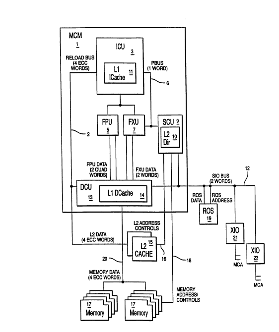
Referring to Figure 2, a block diagram of the overall structure of
the present invention is shown wherein reference numeral 1 represents a
multichip module superscalar processor chip set (CPU), such as is used
in a RISC System/6000 workstation manufactured by IBM Corporation (RISC
System/6000 is a trademark of IBM). Instruction cache unit 3 includes
a branch processing unit 4 (Figure 4) and a level one instruction cache
11. The branch instruction unit (BIU) and branch processing unit (BPU)
processes the incoming instructions and dispatches these instructions to
the floating point unit (FPU) 5 and fixed point unit (FXU) 7. The BPU
provides all of the branching, interrupt, and condition code functions
within the system. Those skilled in the art will understand that FPU 5
executes floating-point instructions while FXU 7 executes fixed point
arithmetic operations (see IBM RISC System/6000 Technology, published by
IBM, 1990, pages 16-42, for a more detailed description of the RISC
System/6000 processing unit).
Storage control unit (SCU) 9 controls access between the CPU and
the level 2 cache 15 and main memory 17. SCU 9 includes a level 2 cache
directory 10 which is used to compare the address of the data or
instructions ("information" as used herein will refer to both data and
instructions) in the L2 cache with the address of the desired
information to determine if a L2 cache hit or miss has occurred. It can
be seen from Figure 2 that SCU 9 does not receive data from either the
L2 cache 15 or memory 17. SCU 9 only provides address and control
information to the L2 and memory. The uni~ue ports from: (1) L2 15 to
DCU 13 and BPU 3; and (2) memory 17 to DCU 13 allow data to be provided
directly to the CPU without the overhead associated with intermediately
storing the data in SCU 9.
Level one data cache unit (DCU) 13 is connected to FPU 5 and FXU 7
and stores recently accessed data which is likely to be needed again by
2142799
-
AT9-94-002 8
the FPU or FXU. DCU 13 includes registers, latches and the like (not
shown), along with the data cache (D-cache) 14 which only stores data.
It can be seen that the architecture of a preferred system implementing
the present invention has separated the L1 cache into a data storage
component 14 and an instruction component (I-cache) 11. In this way,
the data and instructions stored in the L1 cache system are physically
closer to the respective processing units which use data and
instructions. That is, I-cache 11 is in close physical proximity to BPU
3 (contained in ICU 3) such that instructions stored in I-cache 11 can
be easily and quickly provided to, or received from BPU 4. Similarly,
D-cache 14 is located close to FPU 5 and FXU 7 which allows these
execution units ready access to the data stored in D-cache 14. L2 cache
15 is a plurality of static random access memory (SRAMs) devices which
are connected to both the storage control unit 9 and reload hus 2.
Requests for information stored in L2 cache 15 are received from SCU 9,
and if found in the L2, is provided to the requesting processing unit
and the Ll cache along reload bus 2.
The third level of memory is main memory 17 which is a set of
dynamic random access memory devices (DRAMs) which are connected to SCU
9, and DCU 13. Main memory 17 is the slowest memory device in the
system of the present invention, in that it requires the greatest number
of clock cycles to retrieve information therefrom. Memory 17 is
connected directly to DCU 13 which allows information from memory to be
provided directly to FPU 5 and FXU 7. The information is received in
DCU 13 by a register, or the like, and then supplied to the execution
units. Of course, the information from memory 17 could also be provided
to D-cache 14. If instructions are being received from memory 17, the
instruction information is provided from DCU 13 onto reload bus 2 and
then to ICU 3. In this manner data and instruction information can be
provided directly from memory 17 to processing unit 1.
Also shown in Figure 1, is PBUS 6 which transmits the requests for
data or instructions to SCU 9. System input/output bus (SI0)
interconnects DCU 13 (and the various processing units) with the
input/output (I/0) control chips (XI0) 21 and 23. These XI0 chips 21,
- 21~2799
AT9-94-002 9
23 coordinate the transfer of data between an external bus, such as the
Microchannel (MCA) bus (Microchannel is a trademark of the IBM
Corporation) and the internal CPU bus used to interconnect the various
processing units. A read only storage (ROS) chip 19 is shown, also
connected to SIO bus 12, which provides some of the basic routines and
codes used to boot the CPU, such as power on self test (POST) and the
like.
It can be seen from Figures 2 and 4 that ICU 3 not only sends
requests for information to SCU 9, via PBUS 6, but also forwards
instructions to FPU 5 and FXU 7 for execution. Both the FPU 5 and FXU
7 are connected to DCU 13 by two quad word buses for transferring
information between the Ll cache 14 and the processing units. FXU 7 is
also connected to PBUS 6 such that the fixed point unit can also request
information from Ll cache 14. Cache 15 receives address and control
information off of bus 16 (interconnecting it with SCU 9) and is also
connected by reload bus 2 directly to FPU 5 and FXU 7 through register
51 in L1 cache 13 (see Figure 4). Additionally, reload bus 2 directly
connects L2 cache 15 to BPU 4 in ICU 3 through register 50, as shown in
Figure 4. Main memory 17 receives address and control information off
of bus 18 interconnecting it with SCU 9 and is also directly connected
to DCU 13 by bus 20. Figure 2 also illustrates one of the novel
features of the configuration of the present invention in that the L2
cache 15 and memory 17 have a unique port into the processing units and
L1 cache, respectively. Thus, information from memory 17 is not
required to first pass through the L2 cache 15 before being forwarded to
the L1 cache. Additionally, the L2 cache has been connected directly to
the processing units via reload bus 2 and registers in ICU 3 and Ll
cache 13 (see Figure 4). This allows information from L2 cache 15 to be
moved into the requesting execution unit faster than conventional
systems, due to the absence of additional chip crossings. Thus, it can
be seen that the present invention is a non-hierarchical memory system
wherein the L2 cache is directly connected to the processing units, thus
bypassing the L1 cache 13. Further, main memory 17 is directly
connected to Ll cache 13, which bypasses L2 cache 15. When compared
- 21~2799
AT9-94-002 10
with the prior art system of Figure 1, the main memory also bypasses a
memory controller and cache controller such that only a single chip
crossing is needed to provide the requested information to the CPU.
Furthermore, the unique ports of the present invention allows
separation of the memory bus 20 and reload bus 2 such that any bus
loading is minimized. This allows these buses to input information
directly to the CPU, as opposed to a controller, or the like. Thus,
buses 2 and 20 are capable of being operated at a much faster rate, than
conventional systems which tie the entire memory system (e.g. L2 cache
and main memory) directly to a single bus that is connected to the CPU.
Figure 4 shows, in greater detail the non-hierarchical aspect of
the present invention. More specifically, ICU 3 is shown with L1 I-
cache 11 and BPU 4, along with register 50. It can be seen that I-cache
11 is interconnected to branch processor 4 such that instructions are
provided from the cache to BPU 4. Register 50 is directly connected to
reload bus 2 and, thus, to L2 cache 15. The instruction and branch
processor 3 is also connected to FPU 5 and FXU 7 such that the BIU can
dispatch instructions to the floating point and fixed point units. L1
cache 13, including D-cache 14 is shown interconnected to FPU 5 and FXU
7 in order for data required for the execution of instructions by these
processing units can be quickly obtained. DCU 13 also includes a
register 51 which is interconnected to reload bus 2 and L2 cache 15. It
can be seen that a preferred embodiment of the present invention
partitions the Ll cache into I-cache 11 and D-cache 14 for instructions
and data, respectively. These separate partitions are then physically
placed close to the processing units which are most likely to require
the information stored therein. That is, BPU 4 requires instructions,
thus, I-cache 11 is placed near BPU 4. Similarly, FPU 5 and FXU 7
require data, and D-cache 14 is located close to these processing units.
As stated above, conventional hierarchical memory systems provide
information from each level of memory to the next memory level
sequentially until the information finally reaches the requesting
processing unit. However, the present invention allows information
found in a level two cache to be directly provided to the requesting
21~2799
AT9-94-002 1 1
processor. For example, if a L2 cache hit occurs on an instruction
stored therein, the instruction is provided from L2 15 directly to
register 50, via reload bus 2. The instruction is moved into BPU 4 and
I-cache 11 simultaneously during the next cycle. Thus, it can be seen
that the Ll cache is totally bypassed when a cache hit occurs on an
instruction stored in the L2 cache. If the L2 cache hit was for data
information, it would be provided to register 51 and then accessed by
either FPU 5 or FXU 7, without being previously stored in Ll D-cache 14.
Of course, the instruction and data information will be simultaneously
stored in I-cache 11 and D-cache 14, respectively, so that the
information can be more quickly retrieved the next time it is needed,
i.e. information retrieval is faster from the Ll cache than the L2
cache, since the Ll cache is closer to the execution units.
Further, the non-hierarchical nature of the present invention
extends to main memory 17. Conventionally, when Ll and L2 cache misses
occur and the information is found to be in main memory, that
information is then passed to a memory controller, L2 cache controller
and finally to the Ll cache for retrieval by the requesting processing
unit. In contrast, the present invention provides a unique port which
connects the main memory 17 with Ll cache 13 in the CPU, via bus 20.
This direct interconnection of memory 17 with the CPU is implemented by
placing both the memory controller and L2 cache controller in SCU 9,
which only issues address and control signals. As noted above,
conventional systems have a separate cache and memory controller that
receive the requested data and require additional chip crossings before
the data can be provided to the CPU. These additional chip crossings
require a significant amount of overhead in the form of machine cycles
due to the generation of address and control signals, as well as,
intermediately storing the requested data.
More particularly, it can be seen from Figure 4 that memory 17 is
directly connected to register 51 in DCU 13. This allows data
information and instruction information to be provided directly from
memory 17 to register 51. Data information will be accessed by the
execution units 5 and 7 directly from register 51. However, instruction
21~2799
AT9-94-002 12
information will be placed on reload bus 2 for transfer to register 50.
The instruction information is then accessed by BPU 4 from register 50.
The instruction information and data information is also provided to I-
cache 11 and D-cache 14 from registers 50 and 51, respectively, for
later use by the execution units.
Data requested by either FPU 5 or FXU 7 can also be directly
provided from L2 cache 15, via reload bus 2. That is, when data is
requested and a hit occurs in L2 cache 15 the data is placed into
register 51 and then subsequently moved into the requesting processing
unit (FPU 5 or FXU 7) and Ll D-cache 14 during the next cycle. Although
register 51 is physically located in Ll cache chip 13, no Ll latency is
associated with storing data from the L2 cache 15 therein, i.e. there is
no address translation or the like. Thus, the data from L2 cache 15 and
memory 17 bypasses Ll cache 13. In a preferred embodiment, register 51
was placed on the same chip as Ll cache 13 merely for convenience, since
there was space available on that device. It would have been
impractical to redesign the FPU 5 or FXU 7 to include an additional
register. Similarly, providing a separate chip having just a register
therein is also undesirable. Those skilled in the art will understand
that moving requested instructions and data into Ll I-cache 11 and Ll D-
cache 14, respectively will save time, since the information is likely
to be needed again.
Figure 3 is a block diagram of the components which make up SCU 9.
PBUS 6 is shown which transmits requests for information from ICU 3 to
SCU 9. It can be seen that the information requests are placed in both
the L2 request queue 53 and memory request queue 52. Thus, since SCU 9
contains the controller for both the memory 17 and L2 cache 15, the
information request from PBUS 6 can be processed in parallel. When the
request for information exits queue 53, it is input to both L2 cache
directory 10 and comparator 57. The information requested is compared
with the locations in L2 cache 15, i.e. directory 10 outputs address
tags to comparator 57, which then determines if the information in the
cache is that which is requested by ICU 3. If not, a cache miss occurs
and memory operations are allowed to complete, i.e. the main memory is
2l~2799
AT9-94-002 13
searched for the desired information. If the information in the L2
cache is found, by comparator 57 to match the desired information from
queue 53, then a cache hit occurs and a hit signal is sent to L2 cache
controller 55 which in turn sends a stop memory operation signal to
memory controller 59.
The information request from memory request queue 51 is sent to
both memory controller 59 and memory DRAM address translator 61 at the
same time the request is sent from L2 request queue 53 to L2 cache
directory 10. This allows the memory access operations to begin at the
same time the L2 cache is being searched for the requested data. This
provides an advantage since the latency associated with retrieving
information from memory 17 is minimized.
It should be noted that memory controller 59 and L2 cache
controller 55 are on the same integrated circuit (IC) device. This
allows the stop memory operation signal to be provided directly from L2
cache controller 55 to memory controller 59 in a single cycle. Those
skilled in the art will appreciate the enormous savings in cycle time
that occurs when a signal is transferred between components on a single
IC. There is a large amount of overhead associated with transmitted
across chip boundaries. For example, both chips must arbitrate for
ownership of the bus and then implement a transfer protocol. Thus, by
eliminating the chip boundary a large number of clock cycles are saved,
which provide increased performance. That is, when a L2 cache hit
occurs, the stop memory operation signal is received by memory
controller 59 before the memory access operations are complete and any
control signals are output to memory 17 on bus 18. Therefore, when a L2
cache hit occurs, the next memory operation will not be delayed since no
memory operation signals are activated. For example, an MCA adapter
connected to bus 21 or 23 is allowed to continue writing data to main
memory 17 during a DMA transfer with no interruptions due to an
arbitration occurring for ownership of the memory. Additionally, there
is no DRAM perturbation, i.e. the following memory operations are not
held off due to pre-charging of the DRAM.
2l~2~99
AT9-94-002 14
To summarize, not only is the latency associated with memory access
minimized by initiating the L2 cache and memory access simultaneously,
but the memory availability time is also maximized since the memory is
allowed to continue processing when a cache hit occurs. Only when
comparator 57 determines that a cache miss exists is the main memory
even aware that information is being requested.
Eigure 5 is a timing diagram showing the cycles used when an L2
cache miss occurs in a conventional system, such as shown in Figure 1.
In cycle 1, a reload request is placed on data bus 104 and during cycle
2 the conventional cache controller 106 determines that a L2 cache miss
has occurred. Subsequently, a memory controller request signal goes
active during cycle 4 (cycles 3 and 4 were required to communicate the
L2 cache miss signal from cache controller 106 to memory controller 112,
since a chip crossing occurred), and memory arbitration and DRAM address
translation occur during cycle 5 in memory controller 112. In cycles 6
and 7 the Row/Column address is generated, and the row address strobe
(RAS) and column address strobe (CAS) signals are activated at cycles 6
and 7, respectively. When these signals are active, the row and column
address information is on the bus. Information from the memory is
output in cycle 12 to memory controller 112 (on memory data bus 113) and
is placed on data bus 110 (data bus 2 of Figures 1 and 5) during cycle
14. Another chip crossing is then encountered before the retrieved data
can be placed on data bus 104 (data bus 1 of Figures 1 and 5) in cycle
16 and moved into L1 cache 102 in CPU 100. It should be noted that two
clock cycles was used as the time penalty for moving data between chips,
however, other conventional systems may require more than two cycles per
chip crossing. Thus, it can be seen that conventional hierarchical
memory systems require at least 16 cycles in order for information to be
received from main memory when a L2 cache miss has occurred.
~eferring to Figure 6, another timing diagram is shown which
illustrates the sequence of control between L2 cache 15 and the main
memory 17 of the present invention when a cache miss occurs. During
cycle 1, one of the processing units places a reload request on PBUS 6,
as shown by the valid PBUS signal, and in cycle 2 SCU 9 loads the
21~2799
AT9-94-002 15
requested address and performs a L2 cache directory look-up. The
directory tag is compared with bits out of the read address sent on PBUS
6 to determine if the request is a hit or a miss. In parallel, during
cycle 2, memory arbitration and memory DRAM row/column address
generation is performed. In this case it has been assumed that the
cache miss has occurred and the STOP_MEMORY signal is not activated, as
can be seen in Figure 6. Therefore, the memory Row/Column address is
generated during cycles 3 and 4, and the row address strobe signal is
activated in cycle 3. During cycle 4, the column address strobe address
is activated. Thus, at cycle 4, the row and column addresses are on the
bus (bus 18 of Figure 2). These signals are then provided by SCU 9 and
during cycle 9, memory 17 begins driving information onto the memory
data bus 20. At this time, data is provided to DCU 13. If the request
to memory was for data, then the present invention only requires 9
cycles to retrieve the data from memory and make it available to D-cache
14 in DCU 13. However if the request was for instructions, they will be
placed on the reload bus at cycle 11 and available to ICU 11 at this
time. In any event, the information (including data and instructions)
is placed on reload bus 2 at cycle 11 such that the information is
provided to the L2 cache. In this manner, the next time this
information is requested it will be found in the L2 cache and a cache
hit, rather than a L2 cache miss will occur. At cycle 11, the L2 write
enable and chip enable signals are activated to allow the information
to be simultaneously written to L2 cache 15 in parallel with the write
from memory 17 to L1 cache 13 along memory data bus 20 in order to avoid
a future cache miss.
Therefore, it can be seen that the system of the present invention
allows information to be placed in DCU 13 in only 9 cycle (for data) and
on reload bus 2 in only 11 cycles (for instructions), compared to 16
cycles in a conventional system. This is due to the novel aspects of
the present invention which provides a unique port for the memory to
provide information directly to the CPU.
Figure 7 is a timing diagram showing the timing of a conventional
hierarchical memory system, when a L2 cache hit occurs. During cycle 1
2142799
_,
AT9-94-002 16
the requesting processing unit places a reload request on data bus 104,
and in cycle 2, the L2 cache controller 106 does a directory look up and
determines that the information is in the L2 cache. The HIT signal is
activated in cycle 2 indicating that the information to be retrieved is
in the cache. The L2 cache chip enable signal is activated and the L2
address is sent to the L2 cache 108 in cycle 4. In cycle 5, the
retrieved information is output from L2 cache 108 to cache controller
106 in cycle 5. The data is subsequently provided to CPU 100 from data
bus 104 during cycle 7, due to the additional chip crossing required
when the data is provided from L2 cache 108 to cache controller 106,
prior to being placed on bus 104. Thus, it can be seen that with a
conventional hierarchical memory system, at least 7 cycles elapse before
any instructions or data from the L2 cache are placed on data bus 104.
In the prior art shown in Figure 1, the memory access is so slow
that memory operations, e.g. arbitration, memory DRAM address
translation, row/column address generation and the like are not even
initiated, due to the presence of the information in the L2 cache, i.e.
the L2 and memory operations are independent and sequential. However,
other conventional systems may initiate the memory access at the same
time the cache directory is read (cycle 2). In that case at least three
(3) cycles would be added to the memory operations, since an individual
cache controller must send a signal to a separate memory controller.
The present invention, however, combines the cache controller and memory
controller in a single storage control unit (SCU 9) which directly
controls the L2 cache and memory. In this manner, the memory operations
can be aborted before any signals are sent from SCU 9 to memory 17.
Thus, memory 17 may continue normal operations.
Figure 8 is a timing diagram illustrating how the unique port of
the present invention between the L2 cache and the CPU provide data and
instructions to the CPU faster than conventional systems. Additionally,
Figure 8 shows how the memory access is stopped prior to any signals
being output from SCU 9 to the memory 17, when a L2 cache hit occurs.
During cycle 1, one of the processing units, e.g. FXU 7 or BPU 4,
places a reload request on the processor bus PBUS 6 as shown by the PBUS
2142799
-
AT9-94-002 17
valid signal going active. PBUS 6 then transmits the signal to SCU 9.
In cycle 2, SCU 9 loads the address of the requested information and
reads the L2 cache directory 10 to perform an L2 cache directory look-
up. The directory tag from the directory 10 is then compared with bits
from the real address sent on PBUS 6 (using comparator 57 of Figure 3)
to determine if a cache hit or miss has occurred. In parallel, the
memory access operations within SCU 9 are initiated at cycle 2. During
cycle 2 memory arbitration and memory DRAM row/column address generation
is performed. In this case a L2 cache hit has occurred, therefore, a
STOP_MEMORY signal is activated to prevent the memory operation from
ever being started. The STOP_MEMORY signal blocks the memory Row/Column
address from even being generated by SCU 9. Further, the memory RAS and
memory CAS are not sent to the memory (see Figure 6).
During cycle 4, SCU 9 starts the L2 cache read access by activating
the L2 chip enable signal and sending the L2 address from SCU 9 to cache
15. Beginning in cycle 5 the information from L2 cache 15 is driven
onto the reload bus 2 and sent to the requesting processing unit (see
Figure 2). It can be seen from comparing Figures 7 and 8 that
conventional hierarchical memories require 7 cycles to retrieve
information from a L2 cache, but the present invention only requires 5
cycles, thus saving a substantial amount of processing time. This
savings is due to the fact that the unique L2 port allows data to be
transferred directly from the cache to the CPU, rather than through an
intermediate cache controller chip, or the like.
Although certain preferred embodiments have been shown and
described it should be understood that many changes and modifications
may be made therein without departing from the scope of the appended
claims.