Note: Descriptions are shown in the official language in which they were submitted.
wo94/n~03~ 21~ 2 8 6 G PCT/US93/071~2 ;~
METAL ELECTRONIC PACKAGE
I~CORPORATING A MULTI-CHIP MODULE
The present invention relates to metal packages
for housing a plurality of integrated circuit devices.
More particularly, the invention relates to an
adhesively sealed metal package having a circuit:
5 electrically interconnected to a leadf rame and thermally ~;
connected to the package base.
Adhesively sealed metal packages are disclosed in
U.S. Patent Nos. 4,10~,861 to Hascoe; 4,461,92~ to Butt
and 4,939,316 to Mahulikar et al. The packages have a
metallic base and ~o~er. ~ leadframe is disposed
betw~een the base and cover and adhesively bonded to
both. ~The leadframe may include a centrally positioned `
die attach paddle with an integrated circuit device
bonded thereto. Bond wires electrically interconnect
the device to the leadframe.
One advantage of metal packages o~er molded
plastic packages such as quad flat packs (QFPs) or
ceramic packages such as ceramic dual in line packages
(CERDIPs), is improved thermal conduction. The metal ~-
package removes heat generated during the operation of
the device more efficiently than plastic or ceramic
packages. The improved heat dissipation is due to both
the improved thermal conduction of the metallic
components and the ability of the components to disperse
heat laterally along all surfaces of the package~ The
improved thermal dissipation permits encapsulation of
.,, .,, .,, . ~ ~ , . . . . .
W094/05038 21~ 2 8 6 G PCT~US93/071~
~-2-
more comple~ and higher power integrated circuit devices
than is possible with plastic or ceramic packages.
As the integrated circuit devices become more
complex, more electrical interconnections with e~ternal
circuitry and with other integrated circuit devices is
required. The leadframe which electrically
interconnects the device to external circuitry is
usually manufactured from a copper base alloy having a
thickness of from about 0.13mm to about 0.51mm (5-20
mils3. Due to stamping and etching constraints, the
minimum width of each lead, as well as the spacing ~;~
between lead is about equal to the thickness of the
- leadframe. As a result, there is a limit on the number
of leads which may approach the integrated circuit
device~
An additional limitation is lead length. As the
integrated circuit devices become more powerful and
operate at higher operating speeds, the time for an
electronic signal to travel from one device to the nest
limits the speed of the electronic assembly ~such as a
computer). When a single device is encapsulated in each
electronic package, the electronic signal must travel
from the device, through a bond wire, through a
leadframe, through a circuit trace on a printed circuit
board, through a second leadframe, through a second bond
wire and then to a second discretely housed device.
One approach to increase the density of
interconnections to an integrated circuit device and to
reduce the time required for an electric signal to
travel from device to device is a hybrid circuit~ A
hybrid circuit has conductive circuit traces formed on a
dielectric substrate~ Discrete integrated circuit
devices are electrically interconnected to the circuit
traces such that a plurality of devices may all be
~o94/05038 2 1 4 2 8 6 6 PCI/US93/07162
--3--
located on a single substrate. The hybrid circuit can
then be encapsulated in a metal, plastic or ceramic
package typically referred to as a multi-chip module.
E~amples of multi-chip modules, as well as a description
of their development may be found in an article by
Hodson entitled ~Circuits ~eet the Challenge of Size,
Power and Fle~ibility~ which appeared in the October,
1991 issue of ELECTRONIC PACXAGING AND PRODUCTION. -
Multi-chip modules address the problem of
increasing the density of integrated circuit devices.
However, the dielectric substrates which are typically
silicon or alumina, are not ideal for the conduction of
heat from the multi-chip module. While aluminum nitride
has been proposed as an alternate and will provide
better thermal conduction, the material is brittle and
hard to fa~ricate.
Applicants have determined that a low cost, high
- thermal conductivity multi-chip module may be formed
using a metallic sub5trate. The metal, preferably
copper, aluminum or an alloy thereof, has better thermal
conductivity than conventional silicon and alumina
substrates and also better thermal conductivity than
~ovar which is frequently used to house the circuits.
Accordingly, it is an object of the invention to
provide a multi-chip module having high thermal
conductivity. It is a feature of the invention that a
circuit, either rigid or flexible, and either single or
multi-layer, is adhesively bonded to a metallic
substrate with an inorganic dielectric layer disposed
therebetween. A plurality of integrated circuit devices
are electrically interconnected either to that circuit
or to a leadframe positioned around the perimeter of the
circuit. Yet another feature of the invention is that ;`
the devices may be attached to any one of the metallic
W094~5038 2 1 4 2 8 6 6 PCT/US93/071~,
substrate, inorganic dielectric layer, the circuit
traces or an intervening die attach paddle. ~`
It is an advantage of the invention that the
multi-chip modules have high thermal dissipation
5 capabilities. Another advantage of the invention is ~
that the inorganic dielectric layer electrically `
isolates the integrated circuit devices, the adhesively
- bonded ~ircuit and the leadframe from the metallic
package components of the multi-chip module.
In accordance with the invention, there is
provided a leadframe assembly ~or electrically
interconnecting a plurality of semiconductor devices.
The assembly includes a leadframe with inner lead ends ;
defining a central re~ion and a hybrid circuit. The
lS hybrid circuit is made up of a dielectric substrate
which supports circuit traces. The hybrid circuit ;~
contains a first means for electrically interconnecting
at least a portion of the circuit traces to the inner
lead ends of the leadframe and a second means for
supporting a plurality of discrete semiconductor devices.
In a second embodiment of the invention, the
leadframe assembly is encapsulated within metallic
package components or is encased in a plastic molding
resin.
The above stated o~jects, features and ~
advantages, as well as otherst will become more apparent ;
from the specification and drawings which follow.
~igure l shows in cross sectional representation
an adhesively sealed metal package as known from the ~`~
30 prior art. ;~
Figure 2 shows in top planar view an integrated
circuit device bonded to a centrally positioned die
attach paddle as known from the prior art.
wo g4/~038 21 4 2 8 6 G PCT/US93/07162
Figure 3 shows in top plan~r view a hybrid
circuit mounted on a die attach paddle and electrically
interconnected to a leadframe in accordance with a first
embodiment of the invention.
Figure 4 shows in cross sectional representation
a multi-chip module incorporating a centrally positioned ~-
die attach paddle.
Figure 5 shows in cross sectional representation
a hybrid circuit mounted on a metallic package component -~
in accordance with a second embodiment of the invention.
Figure 6 shows in cross sectional representation
a hybrid circuit mounted on a metallic package component
and incorporating a multi-layer circuit in accordance
with a third embodiment of the invention.
Figure 7 shows in cross sectional representation
a multi~chip module with a leadframe is adhesively
bonded to a metallic package component in accordance `~
with a fourth em~odiment of the invention.
Figure 8 shows in cross-sectional representation
20 a hybrid circuit encapsulated in an adhesively sealed ~-
metal package~
The following definitions apply throughout this
application:
Hybrid Circuit - a circuit which combines several
different components in a single package. Typically,
the hybrid circuit will include circuit traces supported ;"
on a dielectric substrate and a plurality of discrete
semiconduc.tor devices.
Multi-Chip Module - an electronic package for
housing one or more hybrid circuits.
Figure 1 shows in cross sectional an adhesively
sealed metal package 10. The package 10 has a metallic
base component 12 and a cover component 14. A leadframe
16 is disposed between the metallic base component 12
W094/05038 ~ 2 1 4 2 8 6 6 PCT/US93/0716~
--6--
and the cover component 14 and adhesively bonded to both
by a polymer adhesive 18.
A die attach paddle 20 which is typically formed
from the same metal as the leadframe is bonded to the `~
metallic base component 12 by a thermally conductive pad
attach adhesive 22. An integrated circuit device 24, -
typically a silicon based semiconductor integrated
circuit, is bonded to the die attach paddle 20 by a die
attach 26 which may be either a low melting temperature
solder or a polymer adhesive. Small diameter bond wires
28 electrically interconnect the leadframe 16 to the ``~
semiconductor device 24. ~-
In the electronic pac~age of U.S. Patent No. ~;`
9,939,316, both the metallic base component 12 and the
co~er component 14 are formed from aluminum or an
aluminum base alloy. At least a portion of the surfaces
30 of the package components is coated with an ~;
anodization layer which provides both corrosion
resistance and electrical isolation. Dependent on
whether the surface 32 of the interior of the metallic
base component 12 is anodized or not, the semiconductor
device 24 may be electrically interconnected to the
metallic base component 12 or electrically isolated ~`
therefrom.
Figure 2 shows in top planar view the positioning ~`
of the semiconductor device 24 on a die attach paddle 20
as known ~rom the prior art. The die attach paddle 20
is disposed within a central region defined by the inner
lead tips 34 of the leadframe. The inner lead tips 34
may approach the semiconductor device 24 from all four
directions as in a quad configuration; from two sides
(dual in-line configuration); or from a single side
(single in-line configuration). Small diameter bond
wires 28 electrically interconnect the semiconductor
W094/~038 ~.- 214 2 8 6 ~ PCT/US93/07162
device 24 to the inner lead ends 34 of the leadframe.
These bond wires 28 are generally smzll diameter,
typically on the order of 0.025mm (~ mil~, wires of
copper, aluminum, gold or alloys thereof and are
thermosonically bonded to the inner lead ends 34 of the
leadframe and metallized input/output pads on the ~`
electrically active face of the semiconductor device
24. Alternatively, thin strips of copper foil as
utilized in tape automated bonding (TAB) may also form
the interconnection between the semiconductor device 24
and the inner lead ends 28.
Due to the stamping and etching constraints
- discussed above, a limited number of inner lead ends 34
may approach the semiconductor device 24. Spacing the
inner lead ends 34 farther from the semiconductor device
24 will permit the inclusion of additional leads, this
is:not a desired solution. As the bond wire length
increases, the operating speed of the de~ice decreases.
Longer bond wires are also prone to sag which may cause
20 an electrical short circuit. These problems are solved :
by the first embodiment of Applicants' invention which
is illustrated in top planar view in Figure 3.
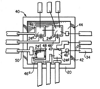
Figure 3 shows a leadframe assembly 40 for the
electrical interconnection of a hybrid circuit 42. The
hybrid circuit 42 comprises a dielectric substrate 44
which supports a plurality of circuit traces 46. The
dielectric substrate 44 may be formed from any suitable
insulative material, either organic or inorganic, and
may be either rigid or fle~ible. Generally, if the
semiconductor devices 24a, 24b, 24C, 24d are
mounted on the dielectric substrate as shown for
semiconductor devices 24a, 24b, 29d, a relatively
thin, on the order of 0.025-0.076mm (1-3 mils),
dielectric substrate is preferred to facilitate the
WOg4/~038 ~ " PCT/~S93/071~,
2142866
-8-
conduction of heat from the semiconductor devices. If
the semiconductor device 24c is mounted in an aperture
48 formed through the dielectric substrate 44 directly
to either the package base (not shown) or a die attach
paddle 20, the thickness of the dielectric substrate
becomes less important. Similarly, if the dielectric
substrate 44 is formed from an insulative material
ha~ing good thermal conductivi~y such as aluminum
nitride or silicon carbide, the thickness of the
substrates is less important.
Typical materials for the dielectric substrate
include ceramics such as alumina (A12O3), aluminum
nitride ~AlN) and silicon carbide (SiC). The dielectric
substrate may also be an organic such as polyimide or an
epo~y, either filled or unfilled. Other substrate
materials include silicon which has good thermal
conductivity and a coefficient of thermal e~pansion
exactly matching that of silicon based semiconductor
devices 24. ~;~
A plurality of circuit traces 46 are formed on
the dielectric substrate 44 by conventional means. For
materials able to withstand high temperatures such as
ceramic and silicon, a desired pattern may be formed
from a metallic paste ~y a process such as screen
printing or direct writing. The metallic paste is then
fired to drive off organic binders leaving behind a
metallized circuit pattern. When the dielectric
substrate 44 is organic based, such as a polyimide, a
metallic film may be deposited by electroless plating or
by lamination of a thin layer of metallic foil.
- Selective etchin~, such as photolithography, forms the
described circuit patterns.
The circuit traces 46 can electrically
interconnect semiconductor devices 24a, 24b. Other
W0941~038 2 1 ~ ~ 8 6 6 PCT~LS93/07162
~,. .. . .
_ g _
.. circuit traces 46' can form a metallization pad for
attachment of an inteqrated circuit device 24a. A
first means is provided to electrically interconnect
circuit trace5 to the inner lead ends 34 of the
5 leadframe. Suit first means include a metallized :~
interposer pad 46~ to shorten the length of bond wires
extending between the inner lead ends 34 of the
leadframe and a semiconductor device 24d.
The circuit traces can form a metallic foil 47
bonded to semiconductor device 24d in TAB format or
for~ a series of discrete bonding sites for direct
soldering to input/output sites on the integrated
circuit device ("flip chip bonding"). ~`
The circuit traces can also form another first
: 15 means for electrical interconnection or an e~tension ~0 -:~
for direct bonding to the inner lead ends 34. The
clrcuit traces 46a can form bonding pads for the
direct attachment of inner lead ends 34 to the hybrid
circuit 42. Attachment may be by any suitable
electrically conductive means such as thermosonic
bonding, thermal compression bonding, soldering and
conductive adhesiYes. Preferred are low melting solders
such as gold tin and lead tin alloys.
Attachment of the leadframe assembly 40 to the
metallic base component 12 of an adhesi~ely sealed metal
package is illustrated in cross-sectional representation
in Figure 4. Figure 4 shows two semiconductor devices
24a, 24c bonded to a die attach paddle 20 by means
of a hybrid circuit 42. Semiconductor device 24a is -
directly bonded to a metallized circuit trace 46'
bonding pad. As more clearly shown in Figure 3,
metallized bonding pad 46' may electrically interconnect
the bac~side of t~e semiconductor device 24a to the
leadframe or to other semiconductor devices.
W094/05038 , ~ ; PCT/US93/071h.
~,'1 42~66
Referring back to Figure 4, the semiconductor
device 24c can e~tend through an aperture 48 in the
hybrid circuit 42 for direct bonding to the die attach
paddle 20. Attachments of the semiconductor devices
S 24a, 24c to either the hybrid circuit 4Z or the die
attach paddle 20 may be by any conventional means such
as an epo~y or a low temperature melting solder. If
electrical interconnection between the backside of the
semiconductor device and the bonding site is desired, -~
10 either a metallic solder such as the gold tin eutectic -~
or a lead tin composition may be used. Alternatively~ a
conductive adhesive such as a silver filled epoay may be
utilized.
If, as illustrated in Figure 3, the integrated
circuit device 24d is directly bonded to the
dielectric substrate 44, suitable die attach materials
include polymer adhesives and, when the dielectric
substrate 44 is a high temperature substrate such as
cera~ic or silicon, a sealing glass may be utilized~
20 Additibnally, metals which alloy with the substrate, for
example, for a silicon substrate gold, may be utilized.
Referring back to Figure 4, two methods of
interconnecting the hybrid circuit 42 to an e~ternal
leadframe are illustrated. Small diameter bond wires 2B
25 electrically interconnect the inner lead ends 34 to a
bondin~ pad 46" which is then electrically
interconnected through a second bond wire 28' to a
semiconductor device 24C. This interposer circuit
structure reduces the length of the bond wire required
30 to interconnect the leadrame to the semiconductor
device 24C.
Alternatively, foil e~tensions 50 may extend from
the circuit metallizations 46 ~or direct interconnection
to inner lead ends 34. Bond 52 between the foil
,, , . , . . . ~ . . . - . . . .
W094/~038 ? . 21 ~ 2 8 6 6 PCT/US93/07162 -~
.extension 50 and the inner lead end 34 may be by any
suitable means which maintains electrical conductivity
between the foil e~tension and the inner lead end such
as a conductive adhesive, a solder or thermal
compressio~ or thermosonic bonding. Most preferred are
low melting temperature solders such as gold-tin or
lead-tin alloys.
The leadframe assembly ~0 is then bonded to a
metallic base component 12 by a pad attach adhesive 22.
The pad attach adhesive 22 may be any suitable metallic
or polymer adhesive such as a solder or eposy. When a
polymer adhesive is utilized, it is desirable to
increase the thermal conductivity of the adhesive to
improve thermal conduction. The pad attach adhesive 22
may be a thermosetting eposy filled with a thermally
conductive material such as silver, graphite or
alumina. One particularly advantageous aspect of this
embodiment is illustrated by the direct bonding of
semiconductor device 24c to die attach paddle 20.
While all the advantages of the hybrid circuit 42 are
obtained, the semiconductor device 24c is in direct
contact with the metallic die attach paddle 20. Heat
generated by the semiconductor de~ice does not pass
through a thermally insulating dielectric substrate 44
to reach the thermally conductive die attach paddle 20.
A second embodiment of the invention is
illustrated in cross sectional representation in Figure
5. The hybrid circuit 42 is bonded such as by an
adhesive 54 directly to the metallic base component 12.
3~ While the dielectric substrate 44 provides electrical
isolation between the circuit traces 46 and the metallic
base component 12, it is desirable to provide an
inorganic dielectric layer 56 between the metallic base
component and the hybrid circuit 42. When the metallic
214286~ `
W094/~038 ~fi~ PCT/US93/071o~
-12-
substrate is aluminum or an aluminum base alloy, the
inorganic dielectric layer may constitute a layer of
anodized aluminum formed by any suitable anodization
process, such as anodic immersion in a solution
containing sulfuric acid and sulfosalicylic acid which
provides an integral black color for aluminum alloys of ~-
the 3~x~ series (aluminum eontaining up to 1.5 weight
percent manganese) as disclosed in U.S. patent No.
5,065,368 to Pasqualoni et al.
Where the metallic base component 12 is copper or
a copper base alloy, the inorganic dielectric layer 56
may constitute a thin refractory oxide layer formed
insitu, by coating with a second material and forming
the inorganic dielectric layer from that second material
or by direct bonding of an insulating layer. The
"insitu" process involves forming the inorganic
dielectric layer 56 directly from the constituents of
the copper base alloy. Preferred copper alloys contain
from about 2 to about 12 percent by weight aluminum.
One particularly preferred alloy is copper alloy C6381
containing 2.~ to 3.1% aluminum, 1.5 to 2.1% silicon and
the balanee copper. The copper base alloy is o~idized
by heating in gases having a low osygen content. One
suitable gas is 4% hydrogen, 96% nitrogen and a trace
of o~ygen released from a trace of water mi~ed in the
gas.
If the copper base alloy is not suited for insitu
formation of the inorganic dielectric layer 56, the
copper base alloy may be clad with a metal or alloy
capable of forming the refractory o~ide. Alternatively,
the copper base substrates may be coated with a second
metal, such as nickel, and a refractory o~ide formed on
the coating layer.
W0~4/05038 2 1 ~ 2 8 6 6 PCT/US93/07162
-13-
Another suitable technique is coating an iron or
copper substrate with a metallic flash of copper or
silver. Aluminum is then electrolytically deposited on
the flash and anodized to form an inorganic dielectric
layer.
Yet another method of forming an inorganic
dielectric layer ~6 on a metallic base component 12 is
soldering an aluminum nitride substrate to a copper
layer using a braze material comprising silver and a
reactive metal selected from the group ~onsisting of
titanium, zirconium and hafnium.
Whatever method is used for the formation of the
- inorganic dielectric layer 56, it is preferred that the
formation of the layer be selective, for e~ample, when
an electrolytic process is used such as anodization, a
plater's tape may mask selected areas to prevent
formation of the layer in those regions. By selective
deposition, semiconductor device 24e may be bonded
directly to the metallic base component 12 to maximize
thermal conduction from the electronic device.
Alternatively, the semiconductor device 24f may be
bonded to the inorganic dielectric layer. The choice
between embodiments 24e and 24f depends on whether ~`
electrical isolation from the metallic base component 12
is desired.
As with the preceding embodiment, the
semiconductor device 24b may be bonded to a `
metallization pad 46' formed from the circuitry traces
46.
Figure 6 illustrates in cross sectional
representation a third embodiment of the invention. In
this embodiment, the hybrid circuit comprises a
multi-layer hybrid circuit 58 having a plurality of
metallic layers and at least one dielectric layer
:
W094/05038 2 ~ 4 ~ g 6 ~ PCT~US93/071~
-14-
separating the metallic layers. Circuit traces 46 may
- be formed on the first metallic layer 60 as well as the
second metallic layer 62. Alternatively, one of the
metallic layers may comprise a solid sheet for use as a
ground or power plane. An electrically conductive via
69 formed by any means known in the art, for e~ample,
deposition of a carbon black dispersion on the walls of
a non-conductive via fol~owed ~y electrolytic or
electroless plating of a conductive material such as
copper may be utilized. The conducti~e vias 6~ allow
electrical interconnection of the second metallic layer
to input/output sites on the face of the semiconductor
device 24b. The semiconductor devices may be bonded
to either of the metallic layers, to the intervening -
dielectric layer 65, to a die attach paddle (not shown)
to the inorganic dielectric layer 56 or to the metallic
base component 12. ~;~
While Figure 6 shows a multi-layer hybrid circuit
58 comprisiny two metal layers and a single dielectric
layer, there may be any number of metallic layers and
intervening dielectric layers. Additionally, while ~`
Figure 6 illustrates an embodiment in which the
multi-layer hybrid circuit 58 is directly bonded to an
inorganic dielectric layer 56 formed on the surface of a `~
25 metallic base component 12, it is within the scope of --
the invention for a die attach paddle to be disposed
between the multi-layer hybrid c;ircuit and the metallic
base component.
Figure 7 illustrates in cross sectional ~-
representation a fourth embodiment of the invention.
The metallic base component 12 has an inorganic
dielectric layer 56 formed on at least one surface. A
thermally conductive, electrically insulating pad attach
adhesive 22 such as a thermosetting polymer,
WO94/05038 1~' 21~`2866 PCI/US93/07162
--15--
thermoplastic polymer or sealing glass bonds both the
inner lead ends 34 of the leadframe and a plurality of
die attach paddles 20 to the metallic base component.
Bond wires 28 electrically interconnect the
semiconductor devices 24 to the leadframe and to
metallic circuit runs 66 which may constitute inner lead
fingers or metallic runs electrically isolated from the -
leadframe.
The semiconductor devi~es 24 are bonded to die
attach paddles 20 with die attach adhesive 26. The die
.
attach paddles are then adhesively bonded to the
inorganic dielectric layer by thermally conductive pad
attach adhesive 22.
The leadframe assemblies illustrated in Figures
3-7 may be encapsulated in any suitable electronic
package, such as plastic, ceramic or metal. Figure 8
illustrates in cross sectional representation a ~:
preferred embodiment in which a multi-layer hybrid
circuit is encapsulated within a metal electronic `
package 70. All elements illustrated in Figure 8 are
not drawn to scale to better show the structure of the
hybrid circuit S8. as a result, certain elements,
notably semiconductor devices 24, are distorted in the
Figure.
The package has a metallic base component 12
formed from a thermally conductive material such as an
aluminum base alloy. Fins 72 may be formed in the
metallic base component 12 to increase thermal
dissipation. A multi-layer hybrid circuit 58 having
30 first 60 and second 62 metallic layers and intervenin~ -
dielectric layers 64 is bonded by adhesive 54 to a die
attach paddle 20. Thermally conductive pad attach
adhesive 22 bonds the multi-layer hybrid circuit and the
die attach paddle 20 to the metallic base component 12.
W094/050~ - ` 2~ 8 6 6 PCT/US93/071~_
-16-
The surface 30 of the base component 12 is preferably
coated with an inorganic dielectric layer to improve
electrical isolation and corrosion resistance. The
first metallic layer 60 contains cantilever foil
extensions 50 for direct bondin~ to the inner leads 34
of leadframe 16. A plurality of semiconductor devices
24 are bonded to the die attach paddle 20. Bond wires
28 electrically interconnec~ the semiconductor devices
24 to circuit traces formed in the first metallic
layer. Electrical interconnection to the second
metallic layer may also be incorporated through the use
of electrically conductive vias (not shown).
A ~over component 14 and a metallic base component
12 are bonded to the leadframe 16 by a polymer adhesive
18. If the polymer adhesive 18 is a thermosetting epo~y
or other adhesive requiring heat for cure, air in the
package cavity 74 will during heating. To prevent the
change in cavity volume from creating pressure on the ;
polymer adhesive 18 and causing an inadequate seal, a
vent hole 76 is preferably formed in the cover component
14. The vent hole 76 is subsequently sealed, for
example, by adhesively sealing a small metal slug to
complete the multi-chip module 70.
While Figure 8 illustrates an embodiment in which
a leadframe assembly is encapsulated within a metal
package, it is within the scope of the invention to
encapsulate any of the above-described leadframe
assemblies in a molded plastic package, a ceramic
package or a glass sealed metal package.
It is apparent that there has been provided in `~
accordance with this invention a leadframe assembly
incorporating a hybrid circuit which fully satisfies the
objects, means and advantages set forth hereinbefore.
While the invention has been described in combination
:
W094/0503~ 2 8 6 6 PCT/US93/0,162
with specific embodiments thereof, it is evident that
many alternatives, modifications and variations will be
apparent to those s~illed in the art in light of the
foregoing description. Accordingly, it is intended to
embrace all such alternatives, modifications, and
variations as fall within the spirit and broad scope of
the claims.