Note: Descriptions are shown in the official language in which they were submitted.
- 2142918
P A T E N T
PD-93125
MICROWAVE WAVEGUIDE MULTIPLEXER
BACKGROUND OF THE INVENTION
Field of the Invention
The present invention relates to waveguide structures for
microwave signal transmission and, more particularly, to
junction elements for microwave waveguide multiplexers.
Background Art
A microwave waveguide multiplexer is a device that either
combines or separates microwave signals of different
frequencies. A typical waveguide multiplexer is fabricated
by joining a filter to a waveguide manifold. The filter is
composed of iris coupled waveguide cavity resonators and
the waveguide manifold is a length of rectangular waveguide
with one end having a metal shorting plate and the other
end connected to a transmit or receive port. In the art,
junctions are usually formed either by a direct connection
of the filter to the broad or narrow wall of the manifold
waveguide or by an additional intermediate length of
rectangular waveguide connected perpendicular to the
manifold and forming a T-junction.
A conventional method of controlling a junction response is
to vary the T-junction distance between the filter and the
manifold by expensive cut-and-try methods. This requires
the development of a breadboard for each design to ensure
that the specifications can be met. Also the T-junction
separation distance needed can be very large, resulting in
a narrow operating frequency band. Since larger microwave
devices have a narrower frequency band over which they
operate successfully, a junction with a step as provided by
the present invention will achieve a wider bandwidth of
CA 02142918 1998-03-0~
operation than a Tjunction.
SUMMARY OF THE INVENTION
An object of an aspect of the present invention is to provide a
microwave waveguide multiplexer wherein the electrical response properties
5 of the waveguide filter-manifold junction of the multiplexer are controlled by the junction design.
An object of an aspect of the present invention is to provide an
improved microwave waveguide multiplexer having a right angle junction
with dimensions selected for controlling the electrical response properties of
10 the junction.
An object of an aspect of the present invention is to provide an
improved microwave waveguide multiplexer having a junction including a
waveguide manifold and a filter connected by a coupling iris and wherein
the electrical response properties of the junction are controlled by a step
15 configuration of the manifold.
An aspect of the invention is as follows:
A method for controlling the electrical response properties of a
waveguide junction, between a filter means and a waveguide multiplexer
manifold structure by reducing the height X of the waveguide junction by a
20 step amount h such that the resultant height of the manifold structure is X-h for the length z of the waveguide junction comprising the steps of:
step 1, providing a calculated equivalent circuit model for said
waveguide multiplexer manifold structure including an impedance inverter
element including first and second pairs of terminals and having a coupling
25 value of K, a pair of shunt susceptance elements each having a value of B
ohms, a first shunt susceptance element connected to one of said second pair
of terminals of said impedance inverter element, and a second shunt
susceptance element connected to the other of said second pair of terminals of
said impedance inverter element, a first transmission line element having a
30 length 1 connected across said first and second shunt susceptance elements
and a second transmission line element having a length 1' connected to said
first pair of terminals of said impedance inverter element, wherein said
CA 02142918 1998-03-0~
2a
coupling value K is the required coupling between the filter means and the
manifold structure and said susceptance elements B represent the additional
elements of the waveguide junction that degrade performance,
step 2, setting the value of B of said susceptance elements of said
5 calculated equivalent circuit to zero for a specified frequency range,
step 3, determining the height h of the waveguide junction step for the
setting of said zero value of B susceptance elements.
BRIEF DESCRIPTION OF THE DRAWINGS
Fig. 1 is a schematic illustration of a microwave waveguide
10 multiplexer according to the principles of the present invention.
Fig. 2 is a schematic illustration of an equivalent circuit diagram for the
junction of the microwave waveguide multiplexer of Fig. 1.
Fig. 3 is a circuit model for a filter-to-manifold with an admittance
inverter.
Figs. 4, 5 and 6 are curves illustrating the electrical
2142918
3 P A T E N T
PD-93125
response of the microwave waveguide multiplexer of Fig. 1.
DESCRIPTION OF THE INVENTION
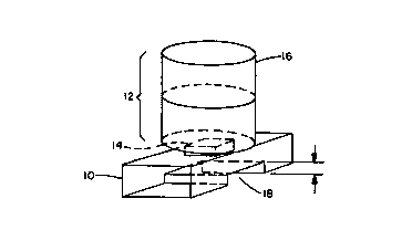
S Referring to Fig. 1 an embodiment of a right angle junction
of waveguides for a microwave multiplexer is shown
including a step in one of the waveguides according to the
present invention for improved electrical response. A
rectangular waveguide manifold 10 is coupled to a filter 12
which includes a coupling iris 14 and a circular cavity
resonator 16.
A circular waveguide is a tubular, circular conductor in
which transverse electric and transverse magnetic modes
propagate. A circular cavity resonator such as resonator
16 is a circular waveguide with two ends closed by a metal
wall.
The embodiment of the present invention shown in Fig. 1
includes a step change 18 in the rectangular waveguide 10
height which controls the electrical response properties of
the junction.
First, a value of the shunt susceptance B is selected.
Typically, it is desired that the structure should have a
susceptance B equal to zero over a specified frequency
range. The designer then varies the height of the step 18
until the value of the shunt susceptance B is set
identically equal to zero at one frequency, normally the
center frequency of the specified frequency range, and the
shunt susceptance B will then ~e approximately equal to
zero over the rest of the frequency range.
More particularly, the changes of the step height 18 of
Fig. 1 produce a resultant response in the form of s-
parameters vs. frequency which is converted to the
CA 02142918 1998-03-0~
equivalent circuit representation of Fig. 2. The equivalent circuit
representation, or model, of the structure of Fig. 1 is composed of an
impedance inverter 20 with value K, a pair of shunt susceptances 22 and 24
each with a value of B ohms, a transmission line 26 of length 1l and a pair of
transmission lines 28, 30 of length 1. The impedance inverter 20 models or
represents the required coupling K between the filter and the manifold. The
susceptances B models or represents the undesired additional elements that
can degrade performance. Susceptance B is determined by the height of the
step 18, so in the technique of the present invention the desired value of B is
10 set equal to zero and the step height for the decided zero value is determined.
The parameters of the configuration of Fig. 1 and its model of Fig. 2 are
obtained and analyzed using electromagnetic simulation software. A
software program entitled HP High-Frequency Structure Simulator (HP
HFSS) which can carry out the analysis is available from the Hewlett-Packard
15 Company, 1400 Fountaingrove Parkway 2US-P Santa Rosa, CA 95403. This
program computes the s-parameters of the configuration shown in Fig. 1 at
specified frequencies. To complete the analysis one skilled in the art can
convert the results into circuit element values for the circuit shown in Fig. 2.Alternatively, an actual device can be constructed and then analyzed
and measured using a microwave network analyzer such as the Hewlett-
Packard Company HP 8510.
As a further aid to one skilled in the art in converting the results of the
analysis of the structure of Fig. 1 into the circuit of Fig. 2, the analysis
program may be coupled to an optimization program such as OSA 90/hope
available from Optimization Systems Associates Inc., 163 Watson's
CA 02142918 1998-03-0~
Lane, Dundas, Ontario, Canada L9HGL1. In such optimization program the
elements of the circuit shown in Fig. 2 can be automatically varied until their
response matches the computed results obtained via simulation such as by
using HP HFSS.
The value K is computed from known circuit design methods for
waveguide or transmission line manifold multiplexers. A program for
computing this value of K is obtaining using the teachings in "Design of
General Manifold Multiplexers" by J. David Rhodes and Ralph Levy, IEEE
Transactions on Microwave Theory and Techniques, Vol. MTT-27, No. 2 Feb.
10 1979, pp 111-123. In this publication, the circuit model for a filter-to-manifold
junction is an admittance inverter of value J, coupled in parallel to a
transmission line or waveguide manifold as shown in Fig. 3. The
configuration from the Rhodes et al publication shown in Fig. 3 is the dual of
that used in the design of the junction shown in Fig. 2 of the present
15 invention, a series coupled impedance inventor of value K. Thus,
numerically a value of J computed in accordance with the teaching of the
Rhodes et al publication equals the value of K used in the circuit of Fig. 2.
Impedance and admittance inverters are common circuit elements used in
Microwave filter design. See "Microwave Filters, Impedance-Matching
20 Networks and Coupling Structures" by George L. Matthaei, Leo Young, and
E.M.T. Jones, McGraw-Hill, New York, NY 1964, pp 431-440.
Having obtained the necessary parameters for the circuit model of Fig.
2, the dimensions of the actual manifold waveguide device depicted in Fig. 1
can be obtained by varying the slot lengths and the step height. The structure
25 of Fig. 1 can be substantially the same as the circuit design of the filter-to-
manifold function of Fig. 2.
CA 02142918 1998-03-0~
Providing the step 18 of the determined height in the waveguide manifold
has the same effect on the structure response characteristics as separating the
T junction distance between the filter 12 and the manifold 10, but has the
advantages of smaller size and wider bandwidth. Thus, the use of the
5 waveguide step 18 becomes important in communications satellite
applications to permit an increase in the number of channel filters that can be
attached to a manifold, and to improve the filter responses.
Figures 4, 5 and 6 show the measured response of a two bandpass
channel multiplexer for first and second bandpass channels using the
10 modified junction of the present invention. Figure 4 shows the common port
return loss; figure 5 shows the insertion loss of the first bandpass channel;
and Figure 6 shows the insertion loss of the second bandpass channel. The
measured responses agree with predictions based on the design model that
assumes B is identically zero.
By increasing the number of channel filters on a manifold, two
multiplexers that cover part of a frequency band can be replaced, typically
every other bandpass channel (an odd-even mutliplexer), with a single
multiplexer that covers the entire band (a contiguous multiplexer). This
allows for replacing a dual feed transmit antenna with a single feed antenna
20 and thereby reducing the weight of the satellite.
The improved filter response permits more stringent system
requirements to be achieved and elimination or reduction of the likelihood of
out-of-spec conditions occurring.
While the invention has been described in connection with a preferred
25 embodiment, it is not intended to limit the scope of the invention to the
particular form set forth, but, on the contrary, it is intended to cover such
~1~2918
7 P A T E N T
PD-93125
alternatives, modifications, and equivalence as may be
included within the spirit and scope of the invention as
defined in the appended claims.