Sélection de la langue

Search

Sommaire du brevet 2142918 

Énoncé de désistement de responsabilité concernant l'information provenant de tiers

Une partie des informations de ce site Web a été fournie par des sources externes. Le gouvernement du Canada n'assume aucune responsabilité concernant la précision, l'actualité ou la fiabilité des informations fournies par les sources externes. Les utilisateurs qui désirent employer cette information devraient consulter directement la source des informations. Le contenu fourni par les sources externes n'est pas assujetti aux exigences sur les langues officielles, la protection des renseignements personnels et l'accessibilité.

Disponibilité de l'Abrégé et des Revendications

L'apparition de différences dans le texte et l'image des Revendications et de l'Abrégé dépend du moment auquel le document est publié. Les textes des Revendications et de l'Abrégé sont affichés :

  • lorsque la demande peut être examinée par le public;
  • lorsque le brevet est émis (délivrance).
(12) Brevet: (11) CA 2142918
(54) Titre français: MULTIPLEXEUR POUR GUIDE D'ONDES HYPERFREQUENCE
(54) Titre anglais: MICROWAVE WAVEGUIDE MULTIPLEXER
Statut: Périmé et au-delà du délai pour l’annulation
Données bibliographiques
(51) Classification internationale des brevets (CIB):
  • H01P 11/00 (2006.01)
  • H01P 01/213 (2006.01)
(72) Inventeurs :
  • HENDRICK, LOUIS W. (Etats-Unis d'Amérique)
  • RAGHAVAN, KRISHNAN (Etats-Unis d'Amérique)
  • SCHWARTZ, CRAIG N. (Etats-Unis d'Amérique)
(73) Titulaires :
  • COM DEV USA, LLC
(71) Demandeurs :
  • COM DEV USA, LLC (Etats-Unis d'Amérique)
(74) Agent: BERESKIN & PARR LLP/S.E.N.C.R.L.,S.R.L.
(74) Co-agent:
(45) Délivré: 1998-09-15
(22) Date de dépôt: 1995-02-20
(41) Mise à la disponibilité du public: 1995-08-23
Requête d'examen: 1995-02-20
Licence disponible: S.O.
Cédé au domaine public: S.O.
(25) Langue des documents déposés: Anglais

Traité de coopération en matière de brevets (PCT): Non

(30) Données de priorité de la demande:
Numéro de la demande Pays / territoire Date
08/198,420 (Etats-Unis d'Amérique) 1994-02-22

Abrégés

Abrégé français

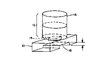
Jonction de guides d'ondes à angle droit pour multiplexeur hyperfréquence, dont un des guides d'ondes comporte un élément de variation en échelon pour améliorer la réponse électrique de la jonction. Un collecteur de guide d'ondes rectangulaire (10) est couplé à un filtre (12) doté d'un iris de couplage (14) et d'un résonnateur à cavité circulaire (16). Ce résonnateur consiste en un guide d'ondes circulaire dont les deux extrémités sont fermées par une paroi métallique. La structure du multiplexeur à guides d'ondes comporte un élément de variation en échelon (18) de la hauteur du guide d'ondes rectangulaire (10), ce qui détermine la réponse électrique de la jonction.


Abrégé anglais


A right angle waveguide junction for a microwave
multiplexer is provided including a step in one of the
waveguides for improved electrical response. A rectangular
waveguide manifold (10) is coupled to a filter (12) which
includes a coupling iris (14) and a circular cavity
resonator (16). The circular cavity resonator is a
circular waveguide with two ends closed by a metal wall.
The structure of the waveguide multiplexer includes a step
change (18) in the rectangular waveguide (10) height which
controls the electrical response properties of the
junction.

Revendications

Note : Les revendications sont présentées dans la langue officielle dans laquelle elles ont été soumises.


THE EMBODIMENTS OF THE INVENTION IN WHICH AN EXCLUSIVE
PROPERTY OR PRIVILEGE IS CLAIMED ARE DEFINED AS FOLLOWS:
1. A method for controlling the electrical response properties of a
waveguide junction, between a filter means and a waveguide multiplexer
manifold structure by reducing the height X of the waveguide junction by
a step amount h such that the resultant height of the manifold structure is
X-h for the length z of the waveguide junction comprising the steps of:
step 1, providing a calculated equivalent circuit model for said
waveguide multiplexer manifold structure including an impedance
inverter element including first and second pairs of terminals and having a
coupling value of K, a pair of shunt susceptance elements each having a
value of B ohms, a first shunt susceptance element connected to one of said
second pair of terminals of said impedance inverter element, and a second
shunt susceptance element connected to the other of said second pair of
terminals of said impedance inverter element, a first transmission line
element having a length 1 connected across said first and second shunt
susceptance elements and a second transmission line element having a
length 1I connected to said first pair of terminals of said impedance
inverter element, wherein said coupling value K is the required coupling
between the filter means and the manifold structure and said susceptance
elements B represent the additional elements of the waveguide junction
that degrade performance,
step 2, setting the value of B of said susceptance elements of said
calculated equivalent circuit to zero for a specified frequency range,
step 3, determining the height h of the waveguide junction step for
the setting of said zero value of B susceptance elements.
2. A method for controlling the electrical response properties of a
waveguide junction according to claim 1 wherein the providing of a
calculated equivalent circuit model includes performing a structure
simulation technique wherein the s-parameters of the said waveguide
multiplexer manifold structure are determined for specified frequencies,
and the elements of said circuit model are determined from said s-

parameters.
3. A method for controlling the electrical response properties of a
waveguide junction according to claim 2 wherein setting the value of B of
said susceptance elements to zero in step 2 of claim 1 is carried out varying
the step height parameter h until the value of said shunt susceptance
elements B is set equal to zero at the center frequency of said specified
frequency range.
4. A method for controlling the electrical response properties of a
waveguide junction according to claim 3 wherein said determining the
height h of said waveguide junction step in step 3 of claim 1 includes
determining the s-parameters of said waveguide multiplexer manifold
structure for said step height at which said shunt susceptance elements B is
equal to zero as determined in claim step 1.

Description

Note : Les descriptions sont présentées dans la langue officielle dans laquelle elles ont été soumises.


- 2142918
P A T E N T
PD-93125
MICROWAVE WAVEGUIDE MULTIPLEXER
BACKGROUND OF THE INVENTION
Field of the Invention
The present invention relates to waveguide structures for
microwave signal transmission and, more particularly, to
junction elements for microwave waveguide multiplexers.
Background Art
A microwave waveguide multiplexer is a device that either
combines or separates microwave signals of different
frequencies. A typical waveguide multiplexer is fabricated
by joining a filter to a waveguide manifold. The filter is
composed of iris coupled waveguide cavity resonators and
the waveguide manifold is a length of rectangular waveguide
with one end having a metal shorting plate and the other
end connected to a transmit or receive port. In the art,
junctions are usually formed either by a direct connection
of the filter to the broad or narrow wall of the manifold
waveguide or by an additional intermediate length of
rectangular waveguide connected perpendicular to the
manifold and forming a T-junction.
A conventional method of controlling a junction response is
to vary the T-junction distance between the filter and the
manifold by expensive cut-and-try methods. This requires
the development of a breadboard for each design to ensure
that the specifications can be met. Also the T-junction
separation distance needed can be very large, resulting in
a narrow operating frequency band. Since larger microwave
devices have a narrower frequency band over which they
operate successfully, a junction with a step as provided by
the present invention will achieve a wider bandwidth of

CA 02142918 1998-03-0~
operation than a Tjunction.
SUMMARY OF THE INVENTION
An object of an aspect of the present invention is to provide a
microwave waveguide multiplexer wherein the electrical response properties
5 of the waveguide filter-manifold junction of the multiplexer are controlled by the junction design.
An object of an aspect of the present invention is to provide an
improved microwave waveguide multiplexer having a right angle junction
with dimensions selected for controlling the electrical response properties of
10 the junction.
An object of an aspect of the present invention is to provide an
improved microwave waveguide multiplexer having a junction including a
waveguide manifold and a filter connected by a coupling iris and wherein
the electrical response properties of the junction are controlled by a step
15 configuration of the manifold.
An aspect of the invention is as follows:
A method for controlling the electrical response properties of a
waveguide junction, between a filter means and a waveguide multiplexer
manifold structure by reducing the height X of the waveguide junction by a
20 step amount h such that the resultant height of the manifold structure is X-h for the length z of the waveguide junction comprising the steps of:
step 1, providing a calculated equivalent circuit model for said
waveguide multiplexer manifold structure including an impedance inverter
element including first and second pairs of terminals and having a coupling
25 value of K, a pair of shunt susceptance elements each having a value of B
ohms, a first shunt susceptance element connected to one of said second pair
of terminals of said impedance inverter element, and a second shunt
susceptance element connected to the other of said second pair of terminals of
said impedance inverter element, a first transmission line element having a
30 length 1 connected across said first and second shunt susceptance elements
and a second transmission line element having a length 1' connected to said
first pair of terminals of said impedance inverter element, wherein said

CA 02142918 1998-03-0~
2a
coupling value K is the required coupling between the filter means and the
manifold structure and said susceptance elements B represent the additional
elements of the waveguide junction that degrade performance,
step 2, setting the value of B of said susceptance elements of said
5 calculated equivalent circuit to zero for a specified frequency range,
step 3, determining the height h of the waveguide junction step for the
setting of said zero value of B susceptance elements.
BRIEF DESCRIPTION OF THE DRAWINGS
Fig. 1 is a schematic illustration of a microwave waveguide
10 multiplexer according to the principles of the present invention.
Fig. 2 is a schematic illustration of an equivalent circuit diagram for the
junction of the microwave waveguide multiplexer of Fig. 1.
Fig. 3 is a circuit model for a filter-to-manifold with an admittance
inverter.
Figs. 4, 5 and 6 are curves illustrating the electrical

2142918
3 P A T E N T
PD-93125
response of the microwave waveguide multiplexer of Fig. 1.
DESCRIPTION OF THE INVENTION
S Referring to Fig. 1 an embodiment of a right angle junction
of waveguides for a microwave multiplexer is shown
including a step in one of the waveguides according to the
present invention for improved electrical response. A
rectangular waveguide manifold 10 is coupled to a filter 12
which includes a coupling iris 14 and a circular cavity
resonator 16.
A circular waveguide is a tubular, circular conductor in
which transverse electric and transverse magnetic modes
propagate. A circular cavity resonator such as resonator
16 is a circular waveguide with two ends closed by a metal
wall.
The embodiment of the present invention shown in Fig. 1
includes a step change 18 in the rectangular waveguide 10
height which controls the electrical response properties of
the junction.
First, a value of the shunt susceptance B is selected.
Typically, it is desired that the structure should have a
susceptance B equal to zero over a specified frequency
range. The designer then varies the height of the step 18
until the value of the shunt susceptance B is set
identically equal to zero at one frequency, normally the
center frequency of the specified frequency range, and the
shunt susceptance B will then ~e approximately equal to
zero over the rest of the frequency range.
More particularly, the changes of the step height 18 of
Fig. 1 produce a resultant response in the form of s-
parameters vs. frequency which is converted to the

CA 02142918 1998-03-0~
equivalent circuit representation of Fig. 2. The equivalent circuit
representation, or model, of the structure of Fig. 1 is composed of an
impedance inverter 20 with value K, a pair of shunt susceptances 22 and 24
each with a value of B ohms, a transmission line 26 of length 1l and a pair of
transmission lines 28, 30 of length 1. The impedance inverter 20 models or
represents the required coupling K between the filter and the manifold. The
susceptances B models or represents the undesired additional elements that
can degrade performance. Susceptance B is determined by the height of the
step 18, so in the technique of the present invention the desired value of B is
10 set equal to zero and the step height for the decided zero value is determined.
The parameters of the configuration of Fig. 1 and its model of Fig. 2 are
obtained and analyzed using electromagnetic simulation software. A
software program entitled HP High-Frequency Structure Simulator (HP
HFSS) which can carry out the analysis is available from the Hewlett-Packard
15 Company, 1400 Fountaingrove Parkway 2US-P Santa Rosa, CA 95403. This
program computes the s-parameters of the configuration shown in Fig. 1 at
specified frequencies. To complete the analysis one skilled in the art can
convert the results into circuit element values for the circuit shown in Fig. 2.Alternatively, an actual device can be constructed and then analyzed
and measured using a microwave network analyzer such as the Hewlett-
Packard Company HP 8510.
As a further aid to one skilled in the art in converting the results of the
analysis of the structure of Fig. 1 into the circuit of Fig. 2, the analysis
program may be coupled to an optimization program such as OSA 90/hope
available from Optimization Systems Associates Inc., 163 Watson's

CA 02142918 1998-03-0~
Lane, Dundas, Ontario, Canada L9HGL1. In such optimization program the
elements of the circuit shown in Fig. 2 can be automatically varied until their
response matches the computed results obtained via simulation such as by
using HP HFSS.
The value K is computed from known circuit design methods for
waveguide or transmission line manifold multiplexers. A program for
computing this value of K is obtaining using the teachings in "Design of
General Manifold Multiplexers" by J. David Rhodes and Ralph Levy, IEEE
Transactions on Microwave Theory and Techniques, Vol. MTT-27, No. 2 Feb.
10 1979, pp 111-123. In this publication, the circuit model for a filter-to-manifold
junction is an admittance inverter of value J, coupled in parallel to a
transmission line or waveguide manifold as shown in Fig. 3. The
configuration from the Rhodes et al publication shown in Fig. 3 is the dual of
that used in the design of the junction shown in Fig. 2 of the present
15 invention, a series coupled impedance inventor of value K. Thus,
numerically a value of J computed in accordance with the teaching of the
Rhodes et al publication equals the value of K used in the circuit of Fig. 2.
Impedance and admittance inverters are common circuit elements used in
Microwave filter design. See "Microwave Filters, Impedance-Matching
20 Networks and Coupling Structures" by George L. Matthaei, Leo Young, and
E.M.T. Jones, McGraw-Hill, New York, NY 1964, pp 431-440.
Having obtained the necessary parameters for the circuit model of Fig.
2, the dimensions of the actual manifold waveguide device depicted in Fig. 1
can be obtained by varying the slot lengths and the step height. The structure
25 of Fig. 1 can be substantially the same as the circuit design of the filter-to-
manifold function of Fig. 2.

CA 02142918 1998-03-0~
Providing the step 18 of the determined height in the waveguide manifold
has the same effect on the structure response characteristics as separating the
T junction distance between the filter 12 and the manifold 10, but has the
advantages of smaller size and wider bandwidth. Thus, the use of the
5 waveguide step 18 becomes important in communications satellite
applications to permit an increase in the number of channel filters that can be
attached to a manifold, and to improve the filter responses.
Figures 4, 5 and 6 show the measured response of a two bandpass
channel multiplexer for first and second bandpass channels using the
10 modified junction of the present invention. Figure 4 shows the common port
return loss; figure 5 shows the insertion loss of the first bandpass channel;
and Figure 6 shows the insertion loss of the second bandpass channel. The
measured responses agree with predictions based on the design model that
assumes B is identically zero.
By increasing the number of channel filters on a manifold, two
multiplexers that cover part of a frequency band can be replaced, typically
every other bandpass channel (an odd-even mutliplexer), with a single
multiplexer that covers the entire band (a contiguous multiplexer). This
allows for replacing a dual feed transmit antenna with a single feed antenna
20 and thereby reducing the weight of the satellite.
The improved filter response permits more stringent system
requirements to be achieved and elimination or reduction of the likelihood of
out-of-spec conditions occurring.
While the invention has been described in connection with a preferred
25 embodiment, it is not intended to limit the scope of the invention to the
particular form set forth, but, on the contrary, it is intended to cover such

~1~2918
7 P A T E N T
PD-93125
alternatives, modifications, and equivalence as may be
included within the spirit and scope of the invention as
defined in the appended claims.

Dessin représentatif
Une figure unique qui représente un dessin illustrant l'invention.
États administratifs

2024-08-01 : Dans le cadre de la transition vers les Brevets de nouvelle génération (BNG), la base de données sur les brevets canadiens (BDBC) contient désormais un Historique d'événement plus détaillé, qui reproduit le Journal des événements de notre nouvelle solution interne.

Veuillez noter que les événements débutant par « Inactive : » se réfèrent à des événements qui ne sont plus utilisés dans notre nouvelle solution interne.

Pour une meilleure compréhension de l'état de la demande ou brevet qui figure sur cette page, la rubrique Mise en garde , et les descriptions de Brevet , Historique d'événement , Taxes périodiques et Historique des paiements devraient être consultées.

Historique d'événement

Description Date
Le délai pour l'annulation est expiré 2013-02-20
Lettre envoyée 2012-02-20
Inactive : Lettre officielle 2009-04-16
Exigences relatives à la nomination d'un agent - jugée conforme 2009-04-16
Inactive : Lettre officielle 2009-04-16
Exigences relatives à la révocation de la nomination d'un agent - jugée conforme 2009-04-16
Lettre envoyée 2009-01-20
Demande visant la révocation de la nomination d'un agent 2008-12-23
Demande visant la nomination d'un agent 2008-12-23
Lettre envoyée 2008-07-30
Lettre envoyée 2007-04-17
Lettre envoyée 2007-02-22
Inactive : Lettre officielle 2007-02-12
Inactive : Lettre officielle 2006-12-05
Inactive : Lettre officielle 2006-12-04
Inactive : TME en retard traitée 2006-10-12
Inactive : CIB de MCD 2006-03-11
Lettre envoyée 2006-02-20
Inactive : Transferts multiples 1999-03-08
Accordé par délivrance 1998-09-15
Inactive : Transferts multiples 1998-08-04
Lettre envoyée 1998-06-30
Exigences de modification après acceptation - jugée conforme 1998-06-30
Inactive : Taxe finale reçue 1998-04-28
Préoctroi 1998-04-28
Inactive : Taxe de modif. après accept. traitée 1998-03-05
Modification après acceptation reçue 1998-03-05
Un avis d'acceptation est envoyé 1997-11-05
Lettre envoyée 1997-11-05
Un avis d'acceptation est envoyé 1997-11-05
Inactive : Renseign. sur l'état - Complets dès date d'ent. journ. 1997-10-29
Inactive : Dem. traitée sur TS dès date d'ent. journal 1997-10-29
Inactive : Approuvée aux fins d'acceptation (AFA) 1997-09-12
Demande publiée (accessible au public) 1995-08-23
Exigences pour une requête d'examen - jugée conforme 1995-02-20
Toutes les exigences pour l'examen - jugée conforme 1995-02-20

Historique d'abandonnement

Il n'y a pas d'historique d'abandonnement

Taxes périodiques

Le dernier paiement a été reçu le 1998-01-22

Avis : Si le paiement en totalité n'a pas été reçu au plus tard à la date indiquée, une taxe supplémentaire peut être imposée, soit une des taxes suivantes :

  • taxe de rétablissement ;
  • taxe pour paiement en souffrance ; ou
  • taxe additionnelle pour le renversement d'une péremption réputée.

Les taxes sur les brevets sont ajustées au 1er janvier de chaque année. Les montants ci-dessus sont les montants actuels s'ils sont reçus au plus tard le 31 décembre de l'année en cours.
Veuillez vous référer à la page web des taxes sur les brevets de l'OPIC pour voir tous les montants actuels des taxes.

Titulaires au dossier

Les titulaires actuels et antérieures au dossier sont affichés en ordre alphabétique.

Titulaires actuels au dossier
COM DEV USA, LLC
Titulaires antérieures au dossier
CRAIG N. SCHWARTZ
KRISHNAN RAGHAVAN
LOUIS W. HENDRICK
Les propriétaires antérieurs qui ne figurent pas dans la liste des « Propriétaires au dossier » apparaîtront dans d'autres documents au dossier.
Documents

Pour visionner les fichiers sélectionnés, entrer le code reCAPTCHA :


Pour visualiser une image, cliquer sur un lien dans la colonne description du document. Pour télécharger l'image (les images), cliquer l'une ou plusieurs cases à cocher dans la première colonne et ensuite cliquer sur le bouton "Télécharger sélection en format PDF (archive Zip)" ou le bouton "Télécharger sélection (en un fichier PDF fusionné)".

Liste des documents de brevet publiés et non publiés sur la BDBC .

Si vous avez des difficultés à accéder au contenu, veuillez communiquer avec le Centre de services à la clientèle au 1-866-997-1936, ou envoyer un courriel au Centre de service à la clientèle de l'OPIC.


Description du
Document 
Date
(aaaa-mm-jj) 
Nombre de pages   Taille de l'image (Ko) 
Abrégé 1995-08-22 1 16
Description 1995-08-22 7 263
Dessins 1995-08-22 3 42
Revendications 1995-08-22 2 62
Description 1998-03-04 8 286
Revendications 1998-03-04 2 71
Dessin représentatif 1998-08-23 1 4
Avis du commissaire - Demande jugée acceptable 1997-11-04 1 165
Avis concernant la taxe de maintien 2006-04-17 1 172
Quittance d'un paiement en retard 2006-10-19 1 166
Avis concernant la taxe de maintien 2012-04-01 1 172
Correspondance 1998-04-12 1 48
Correspondance 1998-04-27 1 56
Taxes 2006-10-11 1 60
Taxes 2006-10-11 1 50
Correspondance 2006-12-04 1 15
Correspondance 2007-02-11 1 20
Correspondance 2007-02-21 1 14
Correspondance 2007-01-22 1 43
Correspondance 2007-04-16 1 16
Correspondance 2007-02-28 2 66
Correspondance 2008-12-22 5 115
Correspondance 2009-04-15 1 13
Correspondance 2009-04-15 1 16
Taxes 1997-01-20 1 64
Correspondance de la poursuite 1995-02-19 9 373