Note: Descriptions are shown in the official language in which they were submitted.
2143074
-1-
A 4 -DQPSK DELAY SPREAD DETECTION
AND COMPENSATION APPARATUS AND METHOD
Background of the Invention
1. Technical Field
The invention relates to digital mobile telecommunications and, more
particularly, to signal receiving circuitry which improves the bit error rate
performance in the presence of interference phenomena.
2. Description of the Prior Art
As demand grows for greater capacity in wireless communication
systems, the telecommunications industry is looking into different approaches
that
will make the limited radio frequency (RF) spectrum currently allocated to
cellular
systems more efficient.
One possible solution to the demand for greater capacity is the digital
systems presently being considered to replace or supplement the existing North
American cellular system which is an analog system. Also known as advanced
mobile phone service or AMPS, the North American cellular system has been
standardized in a number of Telecommunications Industry Association (TIA)
standards, e.g., TR-45.1, and is based upon analog frequency modulation (FM)
technology. This cellular system, however, has the limitation of carrying only
one
voice signal per cellular radio channel.
Typically, in digital wireless communications systems, bandwidth
efficient modulation techniques are used to maximize the amount of information
transmitted in the form of digital voice and data channels. These systems do
so by
reducing the spectral bandwidth required for the transmission of each assigned
channel in the radio frequency spectrum.
One digital cellular system is based upon time division multiple access
(TDMA) techniques and is defined in TIA interim standard (IS)-54. In this
system,
typically 3 to 6 users (data channels) share a common 30 KHz channel. Each
user
transmits data in an assigned time slot that is a part of a larger frame. The
gross bit
rate of the data to be transmitted over the mobile channel is typically 48.6
kilobits
per second (kbps). The modulation method is 4 shifted, differentially encoded,
quadrature phase shift keying (DQPSK).
;2143074
-2-
The combination of digital modulation, error-correcting codes, and
time-slot interleaving provided by the 4 DQPSK technique reduces the effects
of
the most common radio propagation impairments. This, in turn, makes the
limited
RF spectrum currently allocated to cellular systems more efficient, increases
subscriber capacity, and triples the voice channel capacity without requiring
additional RF-spectrum.
The wireless channel, however, consists of a number of interference
phenomena including multipath delay time dispersion or fading, additive white
Gaussian noise (AWGN), co-channel interference and frequency selective fading.
The multipath delay time dispersion in digital communications, for example,
causes
intersymbol interference and also crosstalk between in-phase and quadrature-
phase
signals. This interference phenomena causes imperfections on the wireless
channel
and thus limits the maximum usable transmission rate.
When the multipath delay time dispersion is present at a significant
level, the bit error rate performance of a receiver in the system is
considerably
degraded. The multipath delay time dispersion is characterized by a quality
known as
delay spread. And delay spread, in turn, is the time interval between the
first
arriving signal and last significant echo. It is known in the prior art to
detect delay
spread, as well as co-channel interference. For example, in an article
entitled " In-
Service Monitoring of Multipath Delay-Spread and ClI for QPSK Signal,
published
in Proc. IEEE Vehicular Technology Society Conference (VTC) 1992, pages 592 -
595, S. Yoshida et al. show that the amount of delay spread and also co-
channel
interference on a channel may be detected by monitoring the value of the in-
phase
channel and quadrature channel detector outputs. Similarly, in an article
entitled A
Simple Multipath Delay Time Detection Method for 4 Shift QPSK in Digital
MobilelPortable Communications, published in 41 st IEEE Vehicular Technology
Conference, May 1991, pages 7 -12, B. J. Cho et al. describes an in-service
method
of measuring multipath delay spread which is applicable to a 4 shift QPSK
signal.
In Cho's method, a frequency doubling technique is employed that moves all the
phase states onto the quadrature channel and monitors the in-phase channel for
any
distortion. The circuitry or processing required for implementing the method
of Cho
appears to be rather complex to implement, however. Also, neither Yoshida et
al.
nor Cho et al. provides compensation for multipath delay spread in their
respectively
described schemes.
CA 02143074 1999-07-15
-3-
It is therefore desirable for a receiver in a digital wireless system to
not only be able to detect distortion due to multipath delay spread, but also
be
able to compensate for this distortion in order to improve the bit error rate
performance of such receiver.
Summary of the Invention
In accordance with the invention, a ~/4 delay spread detection and
compensation arrangement effectively detects distortion due to multipath delay
spread on a digital channel and compensates for this distortion with minimum
circuit complexity.
In according with a first aspect of the disclosed embodiment of the
invention, a measured direct current (DC) component signal, which is
proportional to the amount of multipath delay spread on the digital channel,
is
used in compensating for the delay spread in a differential detector in the
receiver. With such compensation, an improvement in the bit error rate
performance for the differential detector is achieved.
In according with a second aspect of the disclosed embodiment of
the invention, the differential detector provides a channel quality measure of
the
level of delay spread on the digital channel. This channel quality measure is
used in selecting either the differential detector or an equalizer for
detecting the
data on the digital channel. When the level of delay spread is low, a
processor
used by the equalizer is freed for other computational tasks or, when the bit
error
rate permits, is not used at all, thereby realizing a reduction in power
consumption in the receiver.
In accordance with one aspect of the present invention there is
provided a digital wireless receiver arranged for decoding digital signals on
a
multipath delay spread digital channel, the receiver comprising: differential
detector circuit means for decoding the digital signals on the channel; means
for
detecting a direct current (DC) component signal produced in the differential
detector circuit means, the level of said DC component signal being
proportional
to the amount of multipath delay spread on the digital channel; and
compensating
means for removing said DC component signal, said compensating means being
responsive to the detecting means for providing compensation to the
differential
detector circuit means for compensating for the multipath delay spread on the
channel.
CA 02143074 1999-07-15
-3a-
In accordance with another aspect of the present invention there is
provided a digital wireless receiver arranged for decoding digital signals on
a
multipath delay spread digital channel, the receiver comprising: differential
detector circuit means for decoding the digital signals on the channel;
equalizer
circuit means for decoding the digital signals on the channel; a moving
average
unit for detecting a direct current (DC) component signal produced in the
differential detector circuit means, the level of said DC component signal
being
proportional to the amount of multipath delay spread on the digital channel;
and
means responsive to the moving average unit for selecting either the
differential
detector circuit means or the equalizer circuit means for decoding the digital
signals on the channel, the selecting means selecting the differential
detector
circuit means when the DC component signal is below a predetermined level and
selecting the equalizer circuit means when the DC component signal is above
the
predetermined level.
In accordance with yet another aspect of the present invention there
is provided a method of decoding digital signals in a wireless receiver, the
digital
signals being received on a multipath delay spread digital channel, the method
comprising the steps of decoding in a differential detector circuit the
digital
signals on the channel; detecting a direct current (DC) component signal
generated in the differential detector circuit, the level of said DC component
signal being proportional to the amount of multipath delay spread on the
digital
channel; and providing compensation to the differential detector circuit in
response to the detecting step for compensating for the multipath delay spread
on
the channel.
In accordance with still yet another aspect of the present invention
there is provided a method of decoding digital signals in a wireless receiver,
the
digital signals being received on a multipath delay spread digital channel,
the
method comprising the steps of: detecting in a moving average unit a direct
current (DC) component signal generated in a differential detector circuit,
the
level of said DC component signal being proportional to the amount of
multipath
delay spread on the digital channel; providing both the differential detector
circuit and an equalizer circuit for decoding the digital signals on the
channel;
and selecting responsive to the detecting step the differential detector
circuit for
CA 02143074 1999-07-15
-3b-
below a predetermined level and selecting the equalizer circuit for decoding
the
digital signals on the channel when the DC component signal is above the
predetermined level.
Brief Description of the Drawings
This invention and its mode of operation will be more clearly
understood from the following detailed description when read with the appended
drawings in which:
FIG. 1 is a model of a typical ~/4 differential quadrature phase-shift
keying communications system and includes a transmitter section, an idealized
multipath frequency selective channel model and a receiver in which the
principles of the invention may be practiced;
FIG. 2 illustrates in flow chart form the program which implements
the principles of the invention in the receiver of FIG. l;
FIG. 3 shows in more detail ~c/4-DQPSK circuitry for use in the
receiver of FIG. l;
_ 2143074
-4-
FIG. 4 provides a graphical illustration of an improvement in
performance obtainable by employing a compensation arrangement achieved in
accordance with an embodiment of the present invention;
FIG. 5 illustrates a relationship between the multipath delay spread in a
digital wireless channel and the DC component signal that may be used in
determining a channel quality estimate; and
FIG. 6 is an illustration of the bit error rate versus signal-to-noise ratio
E
per bit ( Nb ) in dB for normalized excess delay spread of 0.50 ( T ),
compensated
0
and uncompensated, in accord with the principles of the invention.
Detailed Description
Referring now to FIG. 1, there is shown a model of a typical 4
differential quadrature phase-shift keying communications system. The system
includes a transmitter section 110, an idealized multipath frequency selective
channel model 120 and a receiver 150.
Input voice or digital data into the transmitter 110 is provided to a
serial-to-parallel converter circuit 111 in which the even and odd bits are
separated.
The odd bits from the converter circuit 111 are placed on the X k channel and
the
even bits are placed on the Yk channel. Both the odd and even bits,
respectively via
the XK channel and the Yk channel, are coupled to a 4 differential quadrature
phase-shift keying encoder where the carrier is phase shifted according to the
input
data, producing modulated symbols, Ik and Qk. The conventional process
performed in encoder 112 is described in detail in the IS-54 digital cellular
standard
and is, therefore, not further described herein.
From the encoder 112, the modulated symbols, I k and Q k are coupled to
pulse-shaping filters 113 and 114 for generating band-limited, quadrature
component
signals I and Q. These filters may be square root raised cosine transmit pulse
filters
and are described in the IS-54 standard and also described in IEEE
TRANSACTIONS ON VEHICULAR TECHNOLOGY in an article by K. Feher
entitled MODEMS FOR EMERGING DIGITAL CELLULAR-MOBILE RADIO
SYSTEM, Vo1.40, No 2, May 1991, pages 335-365. From the filters 113 and 114,
the
band-limited, quadrature component signals I and Q are provided to a
quadrature
modulator 115 where these quadrature component signals I and Q are modulated
and
coupled onto an RF carrier for transmission at a predetermined frequency.
._ _ 21~~0'~~
-5-
Under ideal conditions, a digital signal transmitted from the transmitter
110 would reach a receiver such as receiver 150 without any fading or
degradation.
However, because of obstructions that may materialize in the path of the
signal,
either while the transmitter is stationary or in motion, such as is the case
while in use
in an automobile, the signal may become distorted. This distortion to the
transmitted
signal occurs when this signal is received via more than one propagation path
of
differing lengths, as caused by the obstructions. Thus multiple images of the
signal
are generated due to reflections from the obstructions. Unfortunately, one or
more of
these multiple images of the signal gets received by a receiver which is then
required
to accurately extract the transmitted information from the distorted signal.
This
negative effect on the transmitted information is illustrated in the frequency
selective
channel model 120.
Channel model 120 shows the transmitted signal input with first and
second independent Rayleigh fading components respectively illustrated in box
121
as fader 1 and in box 122 as fader 2. This channel model 120 is a standard two-
ray
multipath model as recommended by the TIA standards committee and may have up
to a symbol time delay interval between the two rays. The second Rayleigh
fading
component is shown as being delayed by the excess delay of the multipath
channel
and is illustrated in box 123. Although this channel model 120 provides a
worst case
fading environment, it is not to be considered as totally representative of
all delay
spread cases. For example, other channel models may include more multipath
rays
and thereby be more reflective of a particular urban, suburban or bad urban
propagation environment. The channel model 120 is suitable, however, for
generally
illustrating a delay spread profile which requires some type of processing in
order to
recover the distorted transmitted digital signal.
The Rayleigh fading component illustrated in box 121 and the excess
delay obtained at the output of box 123 are summed in a receiving antenna of a
receiver, such as the receiver 150, described later herein. At the antenna
124, the
faded signals are further degraded by the reception of additive white Gaussian
noise
AWGN. Channel model 120 is embodied in the IS-54 standard.
Referring next to the receiver 150 included in a typical 4 differential
quadrature phase-shift keying communications system, the faded digital signals
are
first received in an associated antenna (not shown) and are then coupled into
a
quadrature demodulator 151 in this receiver 150. In the quadrature demodulator
151
the phase modulated carrier is demodulated into its quadrature components I
and Q.
__ _ 2143074
-6-
From the quadrature demodulator 151, the signals I and Q are coupled to pulse-
shaping filters 152 and 153 which are typically cosine filters that limit
noise
bandwidth and also have an impulse response matched to the transmit pulse-
shaping
filters 113 and 114 in the transmitter 110. From the pulse-shaping filters 152
and
153, the band-limited signals, Ik and Qk respectively, are coupled to a 4
differential quadrature phase-shift keying decoder 154. In this decoder 154,
both an
equalizer and a non-coherent, i.e., differential, detector are employed and
selectively
accessed for compensating for delay spread on a digital channel. The operation
of
decoder 154 is described later herein with reference to both the process shown
in
FIG. 2 and the circuitry shown in FIG. 3.
From the decoder 154, the detected and compensated symbols Xk and
Yk are coupled to a parallel-to-serial converter 155, producing a serial
digital, data
stream of the received digital information. The data from the parallel-to-
serial
converter 155 is processed in a conventional manner by being coupled
respectively
to, for example, error correcting and digital voice decoders (not shown).
Finally,
from these decoders, the digital data stream is typically converted into an
analog
form and coupled to, for example, an audio speaker.
With reference now to FIG. 2, there is shown a process which illustrates
the receiver data flow for two modes automatically selectable by the receiver
for
receiving and processing digital data. The process is controlled by a suitably
programmed and readily available commercial processor (not shown) which is
included in the receiver 150.
The process is entered at step 201 where certain processes, such as
course adjustments of automatic gain control, automatic frequency control, and
delay
spread value estimation, are performed. When the process is performed in
accordance with the IS-54 standard, certain slot pre-processing occurs since
data is
transmitted in time-division multiplex slots in the TDMA system defined by
this
standard. This process is also operable in other than a TDMA system, however.
To
be operable in other systems such as , for example, other spread spectrum
systems
and FDMA systems defined by TIA future wireless standards, all that is
required is
that any appropriate pre-processing for another selected system be performed.
From step 201, the process advances to decision 202. In this decision,
the estimated delay spread value is compared to a predetermined threshold Xt.
This
threshold is set at the time of manufacture of the receiver. If the estimated
delay
spread value is greater than the predetermined threshold, the process enters
an
-- 2143074
-7_
equalizer detection processing mode and advances to an equalizer 203. At
equalizer
203, time diversity is extracted from the received frequency selective faded
signal,
thus improving bit error rate (BER) performance. Equalizers are typically
employed
in digital receivers which are affected by multipath delay spreading.
From the equalizer 203, the process advances to an automatic frequency
control unit 204 where frequency offsets in the received signal are minimized.
From
the control unit 204, the process advances to the error correcting decoder
205. This
decoder in the IS-54 standard is typically a Viterbi decoder used to correct
random
bit errors. Such a decoder is disclosed in United States Patent 5,263,052.
From the
decoder 205, the process advances to a digital voice decoder 206 where the
received
bits are decoded into, for example, voice samples for further processing in
other
steps (not shown) by other components in the digital receiver.
Once a time division multiplexed slot has been decoded in the IS-54
standard, the process then returns to step 201 where the next slot is pre-
processed for
subsequent decoding. From the pre-processing step 201, the process again
advances
to the decision 202 where the estimated delay spread value is compared to the
predetermined threshold value. If the estimated delay spread value is less
than the
threshold value, then the process enters the differential detection processing
mode
and advances to the symbol timing recovery unit 207. In this unit, the optimum
sample timing instance is estimated. This includes selecting the proper sample
to be
used for detection and further processing. In the symbol timing recovery unit,
the
optimum sampling instance, i.e., the maximum "eye opening," of the received
signal
is selected in order to obtain reliable data. Channel imperfections are
frequently
evaluated by means of "eye diagrams" or "eye patterns." Such diagrams or
patterns
and an arrangement for obtaining them are described by Dr. K. Kamilo in
Digital
Communications-SatellitelEarth station Engineering, pages 93 - 210, Prentice-
Hall,
1983.
From the symbol timing recovery unit 207, the process advances to
step 208 wherein a base band detector unit such as differential detector 310,
described later herein, is accessed. In this step 208, non-coherent detection
of the
4 -DQPSK signals is performed. A non-coherent detector is employed as the
differential detector rather than a coherent detector because the non-coherent
detector is better in fast fading environments. Some forms of differential
detectors
are described in United States Patent 5,151,926 which issued on September 29,
1992.
- 21430'4
_g_
From step 208, the process advances to an automatic frequency control
unit 209 where frequency offsets in the received signal are minimized. From
step
209, the process advances once again to the error correcting decoder 205 and
on to
the digital voice decoder 206. This process continues for the duration of the
voice
call.
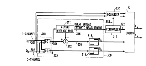
Referring next to FIG. 3, there is shown, in accordance with an
embodiment of the invention, improved 4 -DQPSK differential detector circuitry
300 suitable for use as the differential detector portion of the decoder 154
shown in
FIG. 1. Also shown in Fig. 3 are a controller 317, an equalizer 320 and a
selector
switch 321 which cooperate to provide an advantageous operation when combined
with the differential detector circuitry 300.
This differential detector circuitry 300 may be implemented either in
hardware or in a digital signal processor. An input into the differential
detector
circuitry 300 is provided via a non-coherent, baseband differential detector
310.
These inputs are the Ik signal on the I-Channel and the Qk signal on the Q-
Channel.
The baseband differential detector 310 produces the received data from
differential
phase changes in the received carrier.
The baseband differential detector 310 also performs an autocorrelation
function in the receiver that detects the amount of multipath delay spread
present on
a channel. Mathematically, the baseband differential detector can be
represented as
follows:
Xk-Iklk-1 +QkQk-1 (1~
Yk-Qklk-1 -IkQk-1 (2~
where k = time instant.
Equations 1 and 2 show the use of the autocorrelation function to obtain
the in-phase signal on line 304 and the cross-correlation to obtain the
quadrature
signal on line 303. As the delay spread increases on the digital channel,
equation 1
indicates its presence by computing the sums of the input auto-correlations.
This
sum takes the form of a DC component signal which is proportional to the
amount of
delay spread on the digital channel. The value of the DC component signal
versus
the amount of delay spread on the channel is shown in FIG. 5 for a two ray
channel
_ _214304
-9-
model. From an examination of this figure, a relationship between the delay
spread
and the DC component signal is shown, this relationship being usable as a
channel
quality estimate. In a most economical circuit embodiment using this
autocorrelation function, even a simple level comparator is able to indicate
the
presence of delay spread on a digital channel.
In addition, since it is apparent that the delay spread appears in the form
of a DC component signal on the in-phase signal on line 304, it is also
desirable to
remove this DC component signal in order to improve the BER performance, thus
making the detector 310 more robust in delay spread environments. When the
circuitry of FIG. 3 is employed in the receiver 150 of FIG. 1, an improvement
in the
E
BER vs. Bit Energy per Noise Spectral Density ( Nb ) in dB is provided as
shown in
0
the graph of FIG. 6. In this graph, the ideal performance is shown along with
the bit
error rate curve for normalized excess delay spread of 0.50 ( T ), compensated
and
uncompensated. These curves show the BER performance improvement when using
the compensation arrangement described in FIG. 3. The BER performance
improvement is, for example, approximately 0.5 dB at BER = 1.00E-03.
Referring once again to FIG. 3, The quadrature output signal of detector
310 on line 303 is coupled to a threshold device 314, producing either a 1 or
a -1
output Yk. The in-phase output signal of detector 310 on line 304 is coupled
to both
a moving average unit 311 and to a subtracter 312. The moving average unit 311
estimates the DC component of the signal. This estimated DC component is then
subtracted from the signal on line 304 in the subtracter 312.
The DC compensated in-phase signal on line 306 of FIG. 3 is coupled to
a threshold device 313, producing a 1 or a -1 output Xk. The output of this
threshold
device 313 along with the output of the threshold device 314 are coupled into
a
parallel-to-serial converter, such as the converter 155 shown in FIG. 1.
The estimated DC offset in the moving average unit 311 may be
obtained in either of two ways -- from a moving average filter or a running
average
filter.
In the moving average filter, the final average value is estimated by
sliding a window across the received time slot while measuring the average
value in
the window. In a running average filter, the average value is estimated using
the
entire received time slot data. Moving average units suitable for use as
moving
average unit 311 are known and are described in Digital Signal Process
Principles,
CA 02143074 1999-07-15
-10-
Algorithms, and Applications, by J. G. Proakis et al., 2nd edition, 1992,
pages 102 -
108.
From the moving average unit 311, the delay spread estimate
measurement is provided to controller 317. If the delay spread estimate is
greater
than the predetermined threshold, the equalizer 320 is activated by a signal
from
controller 317 over the control line 318 and the selector switch 321 is also
configured to pass the signal from the equalizer 320 to a parallel-to serial
convener,
such as converter 155 shown in FIG. 1. If the delay spread estimate is less
than the
predetermined threshold, the equalizer is not activated and the signal from
detector 310 is coupled through switch 321.
An equalizer suitable for use as equalizer 320 is disclosed in
United States Patent 5,448,590 issued on September 5, 1995.
Another equalizer is disclosed in United States Patent 5,263,052 which issued
on
November 16, 1993. A general discussion of equalizers is provided in an
article
entitled A comparison of Nonlinear Equalization Methods for the U.S. Digital
Cellular System, by K. L. Baum et al., IEEE-ICC, 1992, pages 291 - 295.
Referring now to FIG. 4, there is shown a graphical illustration of the
differential detector bit error rate in the delay spread channel and the
improvement
obtainable by employing in the differential detector the compensation achieved
by
the embodiment of the present invention. There is also shown, in accordance
with an
embodiment of the disclosed invention, how the best overall improvement in bit
error rate is achieved by employing the differential detector with
compensation and
an equalizer in combination. The method by which this is accomplished is
through a
bimodal operating state selection in the receiver which switches in the
equalizer
when the delay spread value is greater than X~, and for delay spread values
less than
this threshold, use the differential detector. These relationships are
illustrated in
FIG. 4 where the bit error rate BER is shown on the axis of ordinates while
the
normalized delay spread is shown on the axis of abscissas.
When the differential detector is employed without compensation, it
may be seen that the bit error rate (BER) increases rapidly with the presence
of delay
spread in the channel. This is shown by line 401. The differential detector
that is
employed with compensation is shown by line 402. In large delay spreads on a
channel, the bit error rate performance is improved by use of the equalizer as
illustrated by the line 402 in FIG. 4. As recognized by S. H. Good et al. in
IEEE
Vehicular Technology Conference, April 1990, pages 687 - 694, in an article
entitled
A Comparison of Limiter-Discriminator, Delay and Coherent Detection for 4
_ _ 214~~~~
-11-
QPSK, an equalizer performs better when a certain amount of delay spread
exists.
Thus the equalizer's performance starts at a BER floor and improves up to a
point for
increasing delay spreads. The BER floor of a differential detector, both with
and
without compensation is lower than that of the equalizer for small delay
spread.
The differences between the equalizer performance and the non-coherent
detector, without compensation and with compensation, are clearly illustrated
in
FIG. 4. The overall benefit achieved by the embodiment of the present
invention is
that when compensation is employed, the threshold X t can be increased as
shown to
Xt or advantageously set at such level at the time of manufacturer of the
receiver so
that the non-coherent detector is used over a greater delay spread. Since the
detector
is much simpler in circuit complexity, being able to employ this detector over
a
greater range of delay spread advantageously allows a processor used by the
equalizer to be free for other computational tasks in the receiver or, when
the bit
error rate permits, to not be used at all thereby realizing a reduction of
power
consumption in the receiver.
Various other modifications of this invention are contemplated and may
obviously be resorted to by those skilled in the art without departing from
the spirit
and scope of the invention. For example, the co-channel interference which may
appear in the form of a DC component signal on the quadrature output signal
line of
detector 310 may be detected in the manner of the DC component signal on the
in-
phase signal line and similarly used for compensation. Thus it is to be
understood
that the invention may be practiced in ways other than as hereinafter defined
by the
appended claims.