Note: Descriptions are shown in the official language in which they were submitted.
WO 94/07177 PCT/USS°:;r08601
~~ ~3~47
COLOR FILTER SYSTEM FOR DISPLAY PANELS
~ackg~round of the Invention
Flat-panel displays are being developed which
utilize liquid crystals or electroluminescent materials
" 5 to produce high quality images. These displays are
expected t~ supplant cathode ray tube (CRT) technology
and provide a more highly defined television picture.
The most promising route to large scale high quality
liquid crystal displays (LCDs), for example, is the
active-matrix approach in which thin-film transistors
(TFTs) are co-located with LCD pixels. The primary
advantage of the active matrix approach using TFTs is
the elimination of cross-talk between pixels, and the
excellent grey scale that can be attained with
I5 TFT-compatible LCDs.
Flat panel displays employing LCD~s generally
include five different layers: a white light source, a
first polarizing filter that is mounted on one side of
a circuit panel on which the TFTs are arrayed to form
pixels, a filter plate containing at least three
primary colors arranged into pixels, and finally a
second polarizing filter. A volume between the circuit
panel and the filter plate is filled with a liquid
crystal material. This material will rotate the
polarization of light when an electric field is applied
across it between the circuit panel and a ground
affixed to the filter plate. Thus, when a particular
pixel of the display is turned on, the liquid crystal
material rotates polarized light being transmitted
through the material so that it will pass through the
second polarizing filter.
The primary approach to TFT formation over the
large areas required for flat panel displays has
involved the use of amorphous silicon which has
WO 94/07177 PCT/US93/08601
~I436!~'~
-2-
previously been developed for large-area photovoltaic
devices. Although the TFT approach has proven to be
feasible, the use of amorphous silicon compromises
certain aspects of the panel performance. For example,
amorphous silicon TFTs lack the frequency response
needed for large area displays due to the low electron
mobility inherent in amorphous material. Thus, the use
of amorphous silicon limits display speed, and is also
unsuitable for the fast logic needed to drive the
IO display.
Owing to the limitations of amorphous silicon,
other alternative materials include polycrystalline
silicon, or laser recrystallized silicon. These
materials are limited as they use silicon that is
I5 already on glass which generally restricts further
circuit processing to low temperatures. An active
matrix comprising TFTs is also useful in
electroluminescent (EL) displays. The TFTs can be
formed from silicon; however, the same factors that
20 limit the use of polycrystalline silicon and amorphous
silicon in the LCD active matrix also limit the use of
these types of silicon in EL displays. Moreover, EL
displays require TFTs capable not only of high speed
and low leakage, but also of supporting the voltage
25 level needed for electroluminescence.
Thus, a need exists for a method of forming high
quality TFTs at each pixel of a panel display having
the desired speed and providing for ease and reduced
cost of fabrication. Further, a need exists for a
30 method of forming high quality TFTs at each pixel of an
EL panel display having the desired speed and providing
for ease and reduced cost of fabrication, as well has
h
providing the facility to operate the display pixels at
the voltages necessary for luminescence.
~WO 94/07177 ~ PCT/US93/08601
-3-
Summary of the Invention
The present invention relates to panel displays
and methods of fabricating such displays using
thin-films of essentially single crystal silicon in
y 5 which transistors are fabricated to control each pixel
of the display. For a preferred embodiment, the
thin-film or transistor array is transferred
onto an optically transmissive substrate such as glass
or transparent organic films. In this embodiment, the
i0 thin-film single crystal silicon is used to form a
pixel matrix array of thin-film transistors which
actuate each pixel of an LCD. CMOS circuitry that is
highly suitable for driving the panel display can be
formed in the same thin-film material in which the
I5 transistors have been formed. The circuitry is capable
of being fully interconnected to the matrix array using
thin-film metallization techniques without the need for
wires and wirebonding.
Each transistor, by application of an electric
20 field or signal, serves to control the optical
transmission of light from or through an adjacent
material or device. For the purposes of this
application the transistor and the adjacent material or
device through which light from a source is transmitted
25 is referred to as a light valve. Thus, each pixel of
the panel display can be an independently controlled
light valve. Examples of such light valves include LCDs
or any liquid or solid state material whose light
transmitting characteristics can be altered with an
30 electric field or signal and which can be configured to
provide a dense pixel array. The present devices and
related methods of fabrication satisfy all of the
requirements of large scale flat panel to produce
highly defined color images. The transistors or
35 switches can be paired with electroluminescent display
WO 94/07177 214 3 6 4'~ PCT/US93/08601
-4-
elements (ELDs) or light emitting diodes (LEDs) to
provide a display.
A preferred embodiment of the present invention
utilizes large area semiconductor films, separates the
films from the processing substrate, and mounts them on
glass or other suitable optically transmissive
materials. Films of single crystal silicon with
thicknesses on the order of 2 microns sir less, have
been separated from epitaxial substrates, and the films
IO have been mounted on glass and ceramics. Functional p-n
junction devices such as field effect transistors
(FETs) are at least partially fabricated prior to
separation and then transferred to glass. Various
bonding procedures can be used for mounting on
I5 substrates including adhesives, electrostatic bonding,
Van der Waal's forces or a eutectic alloy for bonding.
Other known methods can also be utilized.
A preferred embodiment of the process comprises
the steps of forming a thin essentially single crystal
20 Si film on a release substrate, fabricating an array of
pixel electrodes and thin-film enhancement mode
transistors, and associated CMOS circuitry on the thin
film. Each transistor is electrically connected to one
of the pixel electrodes such that each pixel can be
25 independently actuated by one of the transistors. The
CMOS circuitry can be used to control pixel actuation
and the resulting image or images that are displayed.
Device fabrication can be initiated while the thin-film
is still attached to the release substrate by formation
30 of source, drain, channel and gate regions, and
interconnection with pixel electrodes. By substantially
completing device processing prior to transfer to the
final panel substrate, a low temperature glass or
polymer can be used. Alternatively, all or a portion of
35 device fabrication can occur after release, or upon
WO 94/07177 PCT/US93/08601
-5-
transfer of the processed film to the glass or plastic
plate. After transfer, integration with color filters
and liquid crystal materials completes the panel for an
embodiment employing an LCD.
y 5 Preferred methods of thin-film formation
processes employ silicon-on-insulator (SOI) technology
where an essentially single crystal film is formed on
an insulating substrate from which it can be released.
For the purposes of the present application, the term
"essentially single crystal" means a film in which a
majority of crystals extend over a cross-sectional
area, in the plane extending laterally through the
film, of at least 0.1 cm and preferably in the range of
0.5 -1.0 cmz or more. Such films can be formed using
known techniques, on sapphire, Si02, Si wafers, carbon
and silicon carbide substrates, for example.
SOI technology generally involves the formation
of a silicon layer whose crystal lattice does not match
that of the underlying substrate. A particular
preferred embodiment uses Isolated Silicon Epitaxy
(ISE) to produce a thin film of high quality Si on a
release layer. This process can include the deposition
of a non-single crystal material such as amorphous or
polycrystalline silicon on the release layer which is
than heated to crystallize the material to form an
essentially single crystal silicon. The use of a
release layer enables the film and circuit release
using oxides beneath the active layer that can be
etched without harm to the circuits.
In a preferred embodiment the entire substrate on
which the epitaxial film has been formed is removed by
.
an etch back procedure.
Alternatively, methods of chemical epitaxial
lift-off, a process for transferring semiconductor
WO 94/07177 PCT/US93/08601
-6-
material to glass or other substrates, can be applied
to large area sheets of the desired semiconductor
material. These or other release methods can be used to
remove any thin-film single crystal material from a
growth substrate for transfer onto substrates for
circuit panel fabrication.
The present invention includes CMOS circuit and
pixel electrode formation in a recrystallized silicon
film that is then, secured to a second transfer
substrate, removed from the starting wafer or
substrate, and mounted on the glass or other suitable
substrate to form the circuit panel. Alternatively, one
can first form the circuits, bond the circuits to
glass, and then separate the circuits from the
substrate. The pixels are positioned in rows and
columns having a planar geometry. The order of the
fabrication steps allows the use of conventional fast
CMOS (or other) logic onboard the glass, since the high
temperature processing for these circuits are performed
prior to transfer.
Another preferred embodiment involves the
fabrication of a discrete array of transistor elements,
transferring these elements onto a stretchable
substrate which either contracts or expands to provide
the desired spacing or registration of the discrete
elements and then transferring these elements onto a
final substrate that is including in the display panel.
Other preferred embodiments of the present
invention relate to projection display devices (i.e.
monitors and image projectors) including methods of
fabricating such devices using thin films of single
crystal silicon in which a light valve matrix (or
matrices) is formed for controlling images produced by
these devices. In accordance with the present
invention, projection display devices employing high
~W094/07177 2 ~ ~ PCT/US93/0860t
density single crystal silicon light valve matrices
provide high resolution images compatible with 35 mm
optics.
In one preferred embodiment, an optically
transmissive substrate is positioned to receive light
from a back-light source and a light valve matrix is
secured to the substrate. In accordance with the
present invention, the light valve matrix includes an
array of. transistors and an array of electrodes which
IO are formed in the thin film of single crystal silicon.
The light valve matrix also includes an adjacent light
transmitting material, through which light from the
back-light source is selectively transmitted. Preferred
embodiments are directed to light valves employing a
I5 transmissive light transmitting material such as liquid
crystal or a ferroelectric material, although other
transmissive materials may be used. Each light valve
includes a transistor, an electrode and a portion of
the adjacent light transmitting material. Each
20 transistor, by application of an electric field or
signal, serves to control the optical transmission of
light through the adjacent light transmitting material
for a single light valve.
A driver circuit is electrically connected to the
25 light valve matrix to selectively actuate the light
valves. The drive circuitry may be formed in the same
thin-film material in which the transistors and
electrodes have been formed. The drive circuitry is
capable of being fully interconnected to the matrix
30 using thin-film metallization techniques without the
need for wires and wirebonding. An optical system is
also provided for projecting light transmitted through
the actuated light valves onto a large viewing surface.
The present devices and related methods for
35 fabricating projectors satisfy the requirements of
WO 94/07177 . PCT/US93/08601
_g_
large screen television or monitor displays for
producing highly defined color images. To that end, a
projection display device can have multiple light
valves each adapted to selectively transmit light of a
single primary color. Further, a dichroic prism may be
provided for combining the single color light
transmitted by each light valve producing a multi-color
light image which is projected onto a large viewing
surface.
A preferred embodiment of the formation process
for a light valve matrix employed in a projective
display device comprises the steps of forming a thin
single crystal silicon film which includes forming a
layer of polycrystalline silicon on an insulating
substrate and scanning the polycrystalline layer with a
heat source to crystallize the layer to form a wafer of
single crystal silicon. The process also comprises the
steps of transferring the single crystal silicon film
onto an optically transmissive substrate and attaching
the film to the substrate with an adhesive, forming an
array of transistors, an array of electrodes and drive
circuitry on the silicon film and forming an adjacent
layer of light transmitting material (for example a
liquid crystal material) through which light from a
back-light source may be transmitted. Each transistor
is electrically connected to an electrode such that
each light valve may be independently actuated by one
transistor. The drive circuitry may be used to control
pixel actuation and an optical system is provided for
projecting the resulting images onto a large viewing
surf ace .
In preferred embodiments, the active matrix
circuitry is formed in or on a layer of a semiconductor
material such as silicon. It is noted that any number
of fabrication techniques can be employed to provide
WO 94/07177 ~ PCT/IJS93/08601
_g_
preferred thin-films of polysilicon or single crystal
silicon. In embodiments in which a thin-film of single
crystal silicon is used, extremely high light valve
densities can be achieved such that high resolution
images are obtained. Other embodiments employ the use
s
of a solid state material or any material whose optical
transmission properties can be altered by the
application of an electric field to supply the light
valves of the present invention.
Other preferred embodiments of the present
invention are directed to transmissive and emissive
color displays employing color filters for displaying
color images and methods of fabricating such displays.
In one preferred embodiment, a liquid crystal
transmission display includes an optically transmissive
substrate which is positioned to receive light incident
from a light source. An active matrix circuit panel is
bonded to the optically transmissive substrate such
that the substrate is positioned between the circuit
panel and the light incident from the light source.
The circuit panel comprises a thin film (about 0.1 -
2.0 microns) of an essentially single crystal
semiconductor material such as single crystal silicon.
An array of transistors, an array of pixel electrodes
and a driver circuit are formed in or on the thin film.
Each pixel electrode is electrically connected to a
switching circuit including at least one transistor
such that the circuit panel provides an array of
individually actuated pixel elements. The driver
circuit is electrically connected to each switching
circuit for actuating the pixel elements.
In accordance with the present invention, an
array of color filter elements are formed adjacent to
a
surface of the thin film of essentially single crystal
semiconductor material. Each color filter element is
WO 94/07177 P(.'T/US93/08601
-10-
correlated with a pixel element such that each pixel
element can provide light of a primary color. It is
noted that a primary color is defined herein to
correspond to one of a group of colors which can be
used to provide a spectrum of colors. For example, the ,
color scheme for the array of filter elements can be
red, green and blue or, alternately, yellow, cyan and
magenta, or any other group of colors suitable to
provide the desired spectrum. The color filter
elements are formed by processing an emulsion, a
photoresist, or other suitable carrier in which dyes
can be distributed, or any conventional filter
materials.
A light transmitting liquid crystal material is
positioned adjacent to a surface associated with the
thin film of essentially single crystal material. As
such, the thin film is located between the liquid
crystal material and the color filter array. Further,
a counterelectrode can be formed adjacent to the liquid
crystal material. The liquid crystal material is in
close proximity to the pixel elements such that an
electric field generated across the electrodes of each
pixel element alters a light transmitting property of
the liquid crystal material.
In one embodiment, the filter elements are formed
on an insulating layer which is adjacent to a planar
surface of the thin film and opposite a nonplanar
surface in which the pixel elements are formed. In
another embodiment, the insulating layer is removed
such that the filter elements are formed adjacent to a
planar surface of the thin film. In other preferred
embodiments, the filter elements are formed adjacent to
the nonplanar surface of the thin film in which the
pixel elements are formed. Consequently, the liquid
crystal material is located adjacent to a substantially
WO 94/07177 r ~ ~ ~ ~ ~ PCT/US93/08601
-11-
planar surface of the insulating layer. An advantage
of this construction is that it results in enhanced
performance for the pixels across the display resulting
in sharper displayed images.
The thin film preferably comprises essentially
single crystal silicon material. A matrix array of
opaque (or black) elements can be formed on the thin
film of single crystal silicon such that the opaque
elements are interspersed among the color filter
elements. Each opaque (or black) element serves to
absorb light thereby preventing incident light 'from
impinging upon the transistor or switching circuit
associated with each pixel element.
The active matrix circuit panel is bonded to the
I5 optically transmissive substrate by an adhesive such as
an epoxy or by other methods described in more detail
below. More specifically, an optically transmissive
barrier layer, which comprises a dielectric material
such as a polyimide material or sputtered glass, is
positioned between the array of color filter elements
and the adhesive for isolating the color filter
elements from the adhesive. In other embodiments, the
optically transmissive material can encapsulate the
color filter elements for isolating each ffilter element
from surrounding filter elements, the adhesive and the
thin film.
A preferred embodiment of the fabrication process
for a liquid crystal transmission display comprises
providing a thin film of an single crystal
semiconductor material such as silicon. In one
' embodiment, the processing steps for forming a thin
film of single crystal silicon include forming a layer
of polysilicon over a supporting substrate and scanning
the layer with a heat source to melt and recrystallize
the polysilicon to form a thin film of essentially
WO 94/07177 PCT/US93/08601
2~4364'~
-12-
single crystal silicon. In another embodiment, a
single crystal silicon film or layer can be formed by a
SIMOX (Separation by IMplantation of OXygen) process. .
In another embodiment, the wafer of single crystal
silicon can be secured on a quartz substrate utilizing ,
Van der Waals bonding and the wafer can be thinned
using known techniques to provide the thin film
semiconductor. In yet another embodiment, a bonded
wafer approach can be used to form the layer of thin
IO film single crystal silicon on a single crystal silicon
wafer.
The process also comprises the step of forming an
array of transistors or switching circuits, an array of
pixel electrodes and drive circuitry in or on a front
side of the thin film single crystal silicon such that
each pixel electrode is electrically connected to one
of the switching circuits to provide an active matrix
array of pixel elements. Each pixel element is
actuatable by one of the switching circuits, and the
drive circuitry is used to control pixel actuation.
In accordance with the present invention, the
process includes the step of forming an array of color
filter elements over the front side of the thin film of
essentially single crystal silicon material. Each
color filter element is correlated with one (or more)
of the pixel elements. The color filter elements are
formed by applying a carrier layer such as an emulsion
or a photoresist, including the appropriate dye, on or
over the pixel elements, and then processing the
carrier layer to provide an array of filter elements.
Alternatively, the color filter elements can be formed
by direct deposition of a conventional filter material
such as single layer or multiple layers of thin film
optical coatings. In either case, the layer is then
processed and patterned to produce a resulting color
WO 94/07177 . PCT/US93/08601
~~~~64'~
-13-
filter element adjacent to each of a plurality of pixel
elements for one color. This process can be repeated
to provide different color filter elements for the
remaining pixel elements to produce a multicolor
display.
V.
A matrix array of opaque (or black) elements can
also be formed on or over portions of the thin film of
single crystal silicon such that the opaque elements
are interspersed with the color filter elements. Each
opaque element can be used to define the perimeter of
each pixel element and serves to absorb incident light
that would otherwise impinge upon the switching circuit
associated with the pixel element. Preferably, a layer
of aluminum or the like is also formed over one or both
. 15 side of the thin film and patterned such that each
aluminum element serves as a light shield to reflect
light that may otherwise be directed at the switching
circuits or interconnects to the drive circuitry.
The display fabrication process also includes the
2o step of transferring the thin silicon film, upon which
the active matrix has been formed, and adjacent color
filter array from the supporting substrate onto an
optically transmissive substrate. This will expose a
planar surface which in one embodiment can correspond
25 to an insulating layer adjacent to the back side of the
film or alternatively it will correspond to the back
side of the film if the insulating layer is removed.
The transfer step includes forming an optically
transmissive isolation (barrier) layer, which can
. 30 comprise polyimide, nitride, oxide or sputtered glass,
over the color filter array. The thin film is then
attached to the optically transmissive substrate with
an adhesive such that the isolation layer serves to
isolate the filter elements from each other and the
35 adhesive. A light transmitting liquid crystal material
WO 94/07177 PCT/US93/08601
-14-
is then formed adjacent to the planar surface
associated with the silicon thin film and a
counterelectrode is formed adjacent to the liquid .
crystal material. The counterelectrode is associated
with the array of pixel elements such that an electric
field generated by each pixel element. alters a light
transmitting property of the light transmitting
material.
Yet another preferred embodiment of the present
invention relates to electroluminescent (EL) panel
displays and methods of fabricating such displays using
single crystal silicon materials. Single crystal
silicon is preferred for achieving high resolution in a
small (6 inch by 6 inch or less) active matrix EL
display. In an EL display, one or more pixels are
energized by alternating current (AC) which must be
provided to each pixel by row and column interconnects.
The efficient conduction of AC by the interconnects is
limited by parasitic capacitance. The use of an active
matrix, however, provides a large reduction of the
interconnect capacitance and can enable the use of high
frequency AC to obtain more efficient
electroluminescence in the pixel phosphor and hence
increased brightness. In accordance with the present
invention, the TFTs that provide this advantage are
formed in a single crystal wafer, such as bulk Si
wafers, or thin-films of single crystal or essentially
single crystal silicon. These high quality TFTs are
employed in an EL panel display, providing high speed
and low leakage as well as supporting the high voltage
levels needed for electroluminescence.
Existing EL displays provide a low brightness
output because passive circuitry for exciting pixel
phosphors typically operates at a pixel excitation
frequency (about 100 Hz) that is low relative to the
WO 94/07177 _ ~ ~ ~ ~ PCT/US93/08601
-15-
luminance decay time of the phosphor material. In an EL
display of the present invention, the TFTs are formed
in an active matrix using bulk or thin film single or
essentially single crystal silicon characterized by its
high carrier mobility. As such, the TFTs can operate at
high switching speeds. Thus, the active matrix circuit
panel employing high speed TFTs co-located with the
pixels can provide a high phosphor excitation frequency
relative to the luminance decay time of the phosphor
material resulting in increased brightness of the
display. An EL display of the present invention is
capable of providing a phosphor excitation frequency of
1000 to 10,000 Hz. Preferably, the EL display of the
present invention provides a phosphor excitation
frequency of more than about 5000 Hz and up to about
10,000 Hz leading to a proportionate increase in
luminance.
In preferred embodiments, a thin layer of single
crystal silicon is used to form a circuit panel
comprising an array of transistors and an array of
pixel electrodes, each pixel electrode being actuatable
by one or more transistors. An electroluminescent
material is positioned adjacent to the circuit panel
and patterned to form an array of EL elements. For the
EL display embodiments, each transistor (or transistor
circuit), the associated pixel electrode and the
associated EL material element are referred to as a
pixel. As such, the EL display is comprised of a
plurality of independently controllable pixels. For
each pixel, the transistor (or transistor circuit),
being capable of generating an electric field or signal
across the adjacent EL material, serves to control the
emission of light by the EL material.
CMOS drive circuitry suitable for driving the EL
panel display may be formed in the same single crystal
WO 94/07177 PCT/US93/08601
- -16-
material in which matrices of high voltage DMOS
transistors and pixel electrodes have been formed. The
drive circuitry is capable of being fully .
interconnected to the matrix of pixels using thin-film
metallization techniques without the need for wires and
wirebonding. Further, an optically transmissive
electrode array is positioned over the
electroluminescent material such that the electric
field generated at each pixel lies between the
optically transmissive electrode and the pixel
electrode. As such, each pixel of the EL panel display
can be an independently controlled light emitter whose
light emitting properties are altered by the electric
field or signal.
The present invention comprises devices and
related methods for fabricating EL panel displays
satisfying the requirements for producing high
definition color images. To that end, the
electroluminescent material is used to provide a pixel
that is capable of producing a plurality of different
wavelengths of light. More specifically, the
electroluminescent material can comprise a plurality of
patterned layers, each layer being capable of producing
light of a particular wavelength which is different
relative to the wavelengths produced by other layers
when subjected to the electric field.
A preferred embodiment of the EL display
formation process comprises the steps of forming a
thin-film of single crystal silicon on a supporting
substrate, forming an array of pixel electrodes,
transistors and drive circuitry in or on the silicon
film and forming an electroluminescent structure within
each pixel adjacent to the silicon film. Each
transistor is electrically connected to a pixel
WO 94/07177 ~ ~ PCT/US93/08601
-17-
electrode such that each pixel may be independently
actuated by a drive circuit.
. Preferred methods of single crystal silicon layer
formation processes for an EL display comprise SOI
technology which involves the formation of a silicon
layer on an insulating oxide on a substrate. SoI
structures are preferred because they support the high
voltage, high density circuitry of the EL display of
the present invention. More specifically, the oxide
layer allows the structure to sustain high voltage
devices such as DMOS transistors. Further, the SOI
structure can provide channel isolation for achieving
higher density pixel circuitry which leads to a higher
resolution display.
Other preferred methods relate to thin-film
formation processing for the EL display involving SOI
technology in which a single crystal silicon film is
formed on a support substrate from which it can be
separated and adhered to another material. In one
preferred process, a film of single crystal silicon is
formed on a substrate and active matrix circuitry is
formed in the silicon film. Next, the film is separated
from its substrate and transferred onto a reflective
material for improving light emission of the pixels. In
another preferred embodiment, the film is separated
from its substrate and transferred onto a curved
surface of a material for improved optical properties.
For example, an EL display can be mounted upon a curved
visor of a helmet-mounted system. Alternatively, the EL
display may be mounted onto a curved windshield for a
heads-up display.
In another preferred embodiment, a film of single
crystal silicon is formed on a substrate and the entire
wafer is then attached to a superstrate. Next, the
entire substrate is removed by an etch back procedure.
WO 94/07177 PCT/US93/08601
- -18-
A particular preferred method of the EL display
formation process uses ISE which comprises the steps of
forming a thin essentially single crystal Si film which
includes forming a layer of polycrystalline silicon on
an insulating substrate, forming a capping layer over
the polycrystalline silicon and scanning the
polycrystalline layer with a heat source to
recrystalli2e the layer and form a wafer of
substantially single crystal silicon. The display
formation process further comprises the steps of
forming an array of pixel electrodes, transistors and
drive circuitry in the silicon film and forming an
electroluminescent structure within each pixel. Each
transistor is electrically connected to a pixel
electrode such that each pixel may be independently
actuated by one transistor circuit. The drive circuitry
may be used to control pixel actuation and the
resulting images are displayed.
In another preferred embodiment, an
electroluminescent (EL) color display includes an
active matrix circuit panel formed over a supporting
substrate. As described above, the circuit panel
comprises a thin film (about 0.1 - 2.0 microns) of
single crystal or essentially single crystal
semiconductor material. An array of transistors or
switching circuits, an array of pixel electrodes and a
driver circuit are formed in or on the thin film. An
electroluminescent material is positioned adjacent to
the circuit panel circuitry and patterned to form an
array of EL elements.
For the EL display, each transistor, the
associated pixel electrode and the associated EL
material element are referred to as a pixel element or
light emitter. .For each pixel element, the pixel
electrode is electrically connected to one of the
~WO 94/07177 _ ~ ~ ~ ~ PCT/US93/08601
-19-
transistors which is capable of generating an electric
field or signal across the adjacent EL material causing
the emission of light by the EL material. The driver
circuit can be formed in or on the same single crystal
material as the active matrix circuitry. The driver
circuit is capable of being fully interconnected to the
transistors for actuating the pixel elements using thin
film metallization techniques without the need for
wires and wirebonding.
An optically transmissive electrode is positioned
over the EL structure which can comprise a white
phosphor. As such, the electric field generated at
each pixel element lies between the optically
transmissive electrode and the pixel electrode. An
array of color filter elements is formed adjacent to a
surface of the electrode. Each color filter element is
correlated with one pixel element. The color filter
elements are formed by processing, in accordance with
the techniques described herein, an emulsion, a
photoresist or other suitable carrier in which a dye is
positioned or other conventional filter materials. The
presence of the field causes the EL material to
generate light which passes through the color filter
element to produce a colored light. As such, each
pixel element of the EL display can be an independently
controlled color light emitter whose light emitting
properties are altered by the electric field or signal.
The present invention comprises methods for
fabricating EL displays capable of producing high
definition color images. A preferred embodiment of the
EL display fabrication process comprises providing a
thin film of an essentially single crystal
semiconductor material such as silicon. The processing
steps for forming a thin film of essentially single
crystal silicon include forming a layer of polysilicon
WO 94/07177 PCT/US93/08601
- -20-
over a supporting substrate and scanning the layer with
a heat source to melt and recrystallize the polysilicon
to form a thin film of essentially single crystal
silicon. Alternatively, the single crystal silicon
film or layer can be formed by a SIMOX process, Van der
Waals bonding of a wafer to quartz or a bonded wafer
approach as described in greater detail below.
The process also comprises forming an array of
transistors, an array of pixel electrodes and drive
circuitry in or on the thin film of single crystal
silicon such that each pixel electrode is electrically
connected to one of the transistors to provide an
active matrix array of pixel elements or light
emitters. Each pixel element is actuatable by one of
the transistors, and the drive circuitry is used to
control pixel actuation. The process also includes
forming a layer of EL material (such as a white
phosphor) adjacent to the circuit panel circuitry and
patterning the material to form an array of EL
elements. An optically transmissive electrode is then
formed adjacent to the EL structure. An array of color
filter elements are then formed over the electrode.
Each color filter element is correlated with one (or
more) of the pixel elements.
The color filter elements are formed by applying
a carrier layer such as an emulsion or a photoresist to
the thin film. The carrier layer is then processed and
patterned to produce a resulting color filter element
adjacent to each of a plurality of pixel elements.
This process can be repeated to provide different color
filter elements for the remaining pixel elements to
produce an emissive active matrix color display. A
pattern of opaque (or black) elements can also be
formed such that the opaque elements are interspersed
with the color filter elements. The EL display
WO 94/07177 ~ PCT/US93/08601
-21-
structure is completed by forming an optically
transmissive layer over the color filter array.
The EL display fabrication process can also
include the step of transferring the structure from the
supporting substrate onto an optically transmissive
substrate such as glass, plastic or a head-mounted
visor. The transfer steps can include attaching the
display structure to a temporary substrate, removing
the supporting substrate, attaching the optically
transmissive substrate and removing the temporary
substrate.
A critical advantage provided by the above
referenced methods of color filter fabrication of
display panels is that they provide for precise
alignment of the pixel elements with the filter
elements. Whereas conventional color filter systems
involve alignment of filter elements on the opposite
side of the liquid crystal material, for example, with
the pixel elements in the active matrix when the
laminated structure of the display is finally
assembled, the present system provides for alignment by
fabricating the filter elements directly on the circuit
panel. This provides particular advantages when
utilizing transfer methods as the processing involved
in the transfer can result in some shrinkage of
portions or all of the display thereby making precise
alignment with conventional filter arrays more
difficult.
Brief Description of the Drawinas
The above, and other features of the invention
including various novel details of construction and
combination of parts, will now be more particularly
described with reference to the accompanying drawings
and pointed out in the claims. It will be understood
WO 94/0 ~~ ~ ~~ PC'T/US93/08601
-22-
that the particular panel display and the methods used
in fabricating those panels which embody the invention
are shown by way of illustration only and not as a
limitation of the invention. The principal features of
this invention can be employed in various embodiments
without departing from the scope of the invention.
FIG. lA is an exploded perspective view of a flat
panel display in accordance with the invention.
FIG. 1B is a circuit diagram illustrating the
driver system for a preferred embodiment of the
invention.
FIGS. 2A-2L is a preferred process flow sequence
illustrating the fabrication of a circuit panel for a
flat panel display.
FIG. 3 is a cross-sectional view of a preferred
embodiment of the display panel.
FIG. 4 illustrates in a perspective view a
preferred embodiment of a system used for
recrystallization.
FIG. 5A illustrates the use of a patterned
release layer to entrain boundaries in a crystallized
material.
FIG. 5B illustrates the use of a patterned
capping layer to entrain boundaries.
FIG. 6A illustrates the drain current and
transconductance characteristics for a MOSFET prior to
transfer to glass in accordance with the invention.
FIG. 6B illustrates the drain current and
transconductance characteristics for the MOSFET of FIG.
6A after transfer to glass.
FIG. 7A illustrates the drain current of the
device in FIG. 6A plotted on a logarithmic scale at two _
different drain voltages.
WO 94/07177 . PCT/US93/08601
_213647
-23-
FIG. 7B illustrates the drain current of the
device in FIG. 6B plotted on a logarithmic scale at two
different drain voltages.
FIG. 8A illustrates the drain current output of
the device of FIG. 6A with the gate voltage varying
between O and 5 volts.
FIG. 8B illustrates the drain current output of
the device of FIG. 6B with the gate voltage varying
between O and 5 volts.
FIGS. 9A-9C are a series of cross-sectional
diagrams illustrating a lift-off process in accordance
with the invention.
FIG. lOA is a partial perspective view of a wafer
during lift-off processing according to another
embodiment of the invention.
FIG. lOB is a sectional view taken along lines
II-II of FIG. lOA of the lift-off structure after a
step in the process.
FIG. lOC is a partial perspective view of a
portion of a wafer during lift-off processing in
another embodiment where registration is maintained.
FIGS. lOD and lOE show cross-sections of the
structure of FIG. lOC after additional steps in the
lift-off process.
FIGS. 11A-11E are schematic drawings of a wafer
during various steps in the process flow of a lift-off
procedure in accordance with the invention.
FIGS. 12A-12C are schematic sectional drawings of
another preferred lift-off procedure of the invention.
FIGS. 13A-13C schematically illustrate a
preferred method of transfer in accordance with the
invention.
FIGS. 14A and 14B schematically illustrate
additional transfer methods in accordance with the
invention.
WO 94/07177 PCT/US93/08601
-24-
FIG. 15 illustrates a preferred system for
monitoring and controlling device registration in
accordance with the invention. -
FIG. 16 is a cross-sectional view of a preferred
projection system employed in a high resolution monitor
of the present invention.
FIG. 17 is an illustration of a preferred high
resolution monitor of the present invQntion.
FIG. 18A is an illustration of a high resolution
projection monitor which employs a folded optics
geometry.
FIG. 18B is an illustration of an optical
arrangement which may be employed in the monitor of
FIG. 18A for reducing the thermal losses through the
active matrix.
FIG. 19 is a circuit diagram illustrating the
driver system for a projection device of the present
invention
FIGS. 20A-20D are a preferred process and
transfer sequence for fabricating a light valve matrix
and transferring it to a support structure.
FIGS. 21A-21C are another preferred process and
transfer sequence for fabricating a light valve matrix
and transferring it to a support structure.
FIGS. 22A-22E are yet another preferred process
and transfer sequence for fabricating a matrix and
transferring it to glass substrate.
FIG. 23 is an exploded perspective view of an
active matrix transmission display employing a color
filter system of the present invention.
FIGS. 24A-24C is a preferred process flow
sequence illustrating the SIMOX process for fabricating
a single crystal silicon layer.
FIG. 25 illustrates the Van der Waals bonding
approach for providing a single crystal silicon layer.
WO 94/07177 ~ ~ PCT/US93/08641
-25-
FIGS. 26A-26B is a preferred process flow
sequence illustrating the bonded wafer process for
' forming a single crystal silicon layer.
FIGS. 27A-27G is a preferred process flow
- 5 sequence illustrating the fabrication of a transmissive
active matrix color display.
FIGS. 28A-28K is another preferred process flow
sequence illustrating the fabrication of a transmissive
active matrix color display.
FIG. 29 is a cross-sectional view of the active
matrix color display structure fabricated in accordance
with FIGS. 28A-28K.
FIG. 30A-30H is a process flow sequence using
negative photoresist materials for fabrication of an
array of color filter elements.
FIGS. 31A-31J is a preferred process flow
sequence illustrating in cross-sectional views a
photographic development process for fabricating an
array of color filter elements.
FIGS. 32A-32D is another preferred process flow
sequence illustrating the fabrication of a transmissive
active matrix color display.
FIG. 33A is an exploded perspective view of an
electroluminescent panel display in accordance with the
present invention.
FIG. 33B is a perspective view of an
electroluminescent color display element.
FIG. 33C is a circuit diagram illustrating the
driver system for the electroluminescent panel display.
FIG. 33D is an equivalent circuit for a DMOS
transistor of FIG. 33C.
- FIGS. 34A-34L is a preferred process flow
sequence illustrating the fabrication of a circuit
panel for an electroluminescent panel display.
WO 94/07177 ~ ~ ~~ ~ 4~ . PCT/US93/08601
-2 6-
FIGS. 35A-35D is preferred process flow sequence
illustrating the fabrication of an electroluminescent
color display.
FIGS. 36A-36B is a preferred process flow
sequence illustrating transfer and bonding of an SOI
structure to a superstrate and removal of the
substrate.
FIGS. 37A-37B is a preferred process flow
sequence illustrating an alternative transfer process
in which a GeSi alloy is used as an intermediate etch
stop layer.
FIG. 38 is an exploded perspective view of an
electroluminescent color display in accordance with the
present invention.
FIGS. 39A-39E is a preferred process flow
sequence illustrating the fabrication of an
electroluminescent active matrix color display.
FIGS. 40A-40C is a preferred process flow
sequence illustrating the transfer of an
electroluminescent active matrix color display to an
optically transmissive substrate.
FIG. 4l is an illustration of a patterned pixel
electrode element.
FIG. 42 is an illustration of a head-mounted
active matrix display system.
FIGS. 43A-43E is another preferred process flow
sequence illustrating the fabrication of an
electroluminescent active matrix color display.
FIGS. 44A-44E is another preferred process flow
illustrating the fabrication of a color filter.
FIG. 45 is an illustration of a stacked pixel
element.
WO 94/07177 2 ~ 3 ~ "~ PCT/US93/08601
-27-
Detailed Description of Preferred Embodiments
A preferred embodiment of the invention is
illustrated in the perspective view of a panel display
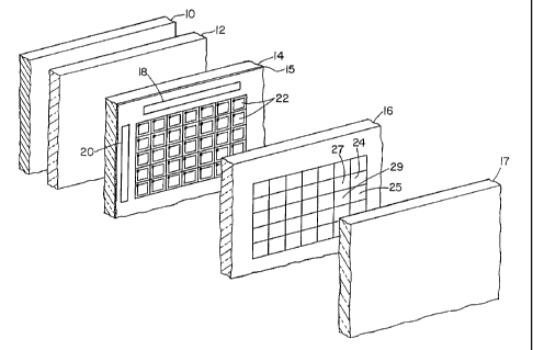
- in FIG. 1. The basic components of the display include
a light source 10 that can be white or some other
' appropriate color, a first polarizing filter 12, a
circuit panel 14, a filter plate 16 and a second
polarizing filter 17, which are secured in a layered
structure. A liquid crystal material (not shown) is
placed in a volume between the circuit panel 14 and the
filter plate 16. An array of pixels 22 on the circuit
panel 14 are individually actuated by a drive circuit
having first 18 and second 20 circuit components that
are positioned adjacent the array such that each pixel
can produce an electric field in the liquid crystal
material lying between the pixel and a counterelectrode
secured to the color filter plate 16. The electric
field causes a rotation of the polarization of light
being transmitted across the liquid crystal material
that results in an adjacent color filter element being
illuminated. The color filters of filter plate system
16 are arranged into groups of four filter elements
such as blue 24, green 25, red 27, and white 29. The
pixels or light valves associated with filter elements
24, 25, 27, 29 can be selectively actuated to provide
any desired color for that pixel group.
The present invention employs any transmissive or
emissive material to form each pixel of the display
panel. To that end, some preferred embodiments employ
the use of a liquid, such as the aforementioned liquid
- crystal material, to form a transmissive light valve
for each pixel. Other preferred embodiments employ the
- use of a solid state material such as a ferroelectric
material to form a transmissive light valve for each
pixel. Further, other preferred embodiments employ the
WO 94/0~~7~~ ~ ~~ PCT/US93/08601
-28-
use of other solid state materials to form a light
emitter for each pixel. An electroluminescent film,
porous silicon or any light emitting material whose
optical transmission properties can be altered by the
application of an electric field can be used to form
the light emitter. Accordingly, electroluminescent
display elements (ELD), porous silicon display elements
or light emitting diodes can be formed and used to
provide a display.
A drive circuit that can be used to control the
display on the panel is illustrated in FIG. 1B. Circuit
18 receives an incoming signal and sends a signal to
the pixels through buses 13. Circuit 20 will scan
through buses 19 to turn on the individual transistors
23 which charges capacitor 26 in each pixel. The
capacitor 26 sustains the charge on the pixel electrode
and the liquid crystal 21 until the next scan of the
array. The various embodiments of the invention may, or
may not, utilize capacitors with each pixel depending
upon the type of display desired.
FIGS. 2A-2L illustrate the use of an Isolated
Silicon Epitaxy (ISE) process, to form
silicon-on-insulator (SOI) films in which circuit panel
circuitry is formed. Note that any number of techniques
can be employed to provide a thin-film of single
crystal Si. An SOI structure, such as that shown in
FIG. 2A, includes a substrate 30 and an oxide 34 (such
as, for example, Si02) that is grown or deposited on
the substrate 30. A thin single crystal layer of
silicon is formed over the oxide 34. The oxide (or
insulator) is thus buried beneath the Si surface layer.
For the case of ISE SOI structures, the top layer is a
substantially single-crystal recrystallized silicon,
from which CMOS circuits can be fabricated. The use of
WO 94/07177
PCT/US93/08601
-29-
a buried insulator provides devices having higher
speeds than can be obtained in conventional bulk
(Czochralski) material. Circuits containing in excess
of 1.5 million CMOS transistors have been successfully
fabricated in ISE material.
As shown in FIG. 2B, the film 38 is patterned to
define a transistor region 37 and a pixel electrode
region 39 for etch pixel. An oxide layer 40 is then
formed over the patterned regions including channel 48
between the two regions 37, 39 of each pixel. The
intrinsic crystallized material 38 is than implanted 44
(at FIG. 2C) with boron or other p-type dopant to
provide a n-channel device (or alternatively, an n-type
dopant for an p-channel device).
A polycrystalline silicon layer 42 is than
deposited over the pixel and the layer 42 is then
implanted 46, as seen in FIG. 2D, with an n-type dopant
to lower the resistivity of the layer 42 to be used as
a gate. The polysilicon is patterned to form the gate
50, as seen in FIG. 2E, which is followed by a large
implant 52 of boron to provide p+ source and drain
regions for the transistor. As shown in FIG. 2F, an
oxide 54 is formed over the transistor and openings 60,
56, 58 are formed through the oxide 54 to contact the
source 66, the drain 64, and the gate, respectively. A
patterned metalization 70 of aluminum, tungsten or
other suitable metal is used to connect the exposed
pixel electrode 62 to the source 60 (or drain), and to
connect the gate and drain to other circuit panel
components.
A second fabrication procedure is one of the
substrate release processes that have been developed to
form thin (1 to 5 micron) films of processed silicon
bonded to glass; these films contain active
semiconductor devices such as FETs that are partially
CA 02143647 2003-02-10
W~ 94/07177 PCT/US93/08601
-30-
of completely fabricated prior to transfer. The
crystallization and release procedures including the
cleavage of laterally grown epitaxiai films for
transfer (CLEFT) approach are described more fully in
U.S. Patent No. 4,727,047.
The chemical epitaxial lift-off (CEL)
approach is described more fully in U.S. Patent Nos.
4,846,931 and 4,883,561. Both of the CLEFT and CEL
techniques permit the reuse of the substrate, leading
to reduced cost compared to other approaches in which
the substrates are consumed. By combining thin film
release techniques with SOI wafers, we are able to form
the required high quality films and circuits on glass.
The foregoing indicates that CEL processes can be
limited by the lateral distance that is required for
the HF (or other etchant) undercut of the release
layer. The key to large area panels using CEL is the
release of patterned devices and/or circuits rather
than complete large-area films, because the circuits or
devices have unused areas that can be used as vertical
channels through the film to allow the etch to reach
the release layer. This approach is illustrated in
FIGS. 2H-2L. To remove the circuit from the release
substrate a first opening 70 (in FIG. 2H) is formed in
an exposed region of layer 36 that occurs between
pixels. A second larger portion of layer 34 is than
removed to form cavity 72 such that a portion of layer
36 extends over the cavity 72.
In FIG. 2I, a support post ?6 is formed to fill
cavity ?2 and opening 70, and which extends over a
portion of layer 36. Openings or via holes 74 are then
provided through layer 36 such that an etchant can be
introduced through holes 74, or lateral openings 78, to
remove layer 34 (see FIG. 2J). The remaining insulating
layer 36 and the circuitry supported thereon are row
WO 94/07177 ~ ~ ~ ~ ~ pCT/US93/08601
-31-
held in place relative to substrate 30 with support
posts 76.
An epoxy that can be cured with ultraviolet light
- is used to attach an optically transmissive substrate
80 to the circuitry, and layer 36. The substrate 80 is
than patterned such that regions of epoxy 84 about the
posts 76 remain uncured while the remaining epoxy 82 is
cured (see FIG. 2K). The substrate 30 and posts 76 are
removed to provide the structure shown in FIG. 2L,
which is then processed to provide the desired display
panel.
Note that the W-cured adhesive (or tape) can be
patterned to protect the circuits where necessary, and
HF can be used to reach the remaining the release
layer.
Note that where tape is used, tape provides
support to the circuits after release. Large area GaAs
devices containing films have been fabricated in this
way, and these have been released to form devices from
entire wafers on one tape. The released circuits can be
remounted on the glass and the other elements of the
liquid crystal display panel. Transparent adhesives are
the preferred method of mounting.
To form the final display panel the circuit panel
shown in FIG. 2L is etched leaving the desired pixel
elements exposed. Insulation and alignment layers,
spacers, a sealing border and bonding pads for
connections as added onto the circuit panel. A screen
printing process can be used to prepare the border. The
plate containing the color filters and the
counterelectrode is sealed to the circuit panel with
the sealing border after insertion of spacers. The
- display is filled with the selected liquid crystal
material via a small filling hole or hole extending
through the border. This filling hole is then sealed
WO 94/07 ~ ~ ~~ ~ ~~ PCT/US93/08601
-32-
with a resin or epoxy. First and second polarizer films
or layers are than bonded to both sides and connectors
are added. Finally, a white light source 114, or other
suitable'light source, is coupled to polarize 112.
A cross-sectional view of the resulting device is
shown in FIG. 3 wherein pixel electrodes 102 and 104
are laterally spaced from each other. Each pixel
electrode 102, 104 will have a transistor 106 and a
color filter 120, 122 associated therewith. Polarizing
elements 112, 118 are positioned on opposite sides of
the structure which also includes bonding element or
adhesive 108 and optically transmissive substrate 110,
such as glass or plastic. Layer 108 can be a
transparent epoxy or a low temperature glass that can
have a thickness of 2-10 microns.
The CLEFT process permits the separation of a
thin single-crystal films, grown by chemical vapor
deposition (CVD), from a reusable homoepitaxial
substrate. Unlike the CEL process, in the CLEFT process
the circuits or devices are first bonded to glass and
after mounting the separation is made between the
circuits and the substrate.
The films removed from the substrate by CLEFT are
essentially single-crystal, of low defect density, are
only a few~microns thick, and consequently the circuit
panel has little weight and good transmission
characteristics. For the purposes of the present
application, the term "essentially single crystal"
means a film in which a majority of crystals extend
over a cross sectional area in a plane of the film of
at least 0.1 cm2, and preferably in the range of 0.5 - '
1. 0 cmz or more .
The CLEFT process, illustrated in U.S. Patent No. '
4,727,047 involves the following steps: growth of the
WO 94/07177 PCT/US93/08601
-33-
desired thin film over a release layer (a plane of
weakness), formation of metallization and other
coatings, formation of a bond between the film and a
second substrate such as glass (or superstrate), and
separation along the built-in-plane of weakness by
cleaving. The substrate is then available for reuse.
The CLEFT process is used to form sheets of essentially
single crystal material using lateral epitaxial growth
to form a continuous film on top of a release layer.
IO For silicon the lateral epitaxy is accomplished by the
ISE process or other recrystallization procedures.
Alternatively, other standard deposition techniques can
be used to form the necessary thin-film essentially
single crystal material.
I5 One of the necessary properties of the material
that forms the release layer is the lack of adhesion
between the layer and the semiconductor film. Since a
weak plane has been created by the release layer, the
film can be cleaved from the substrate without any
ZO degradation. The release layers can comprise
multi-layer films of Si3N4 and Si02. Such an approach
permits the SiOz to be used to passivate the back of
the CMOS logic. (The Si3N4 is the layer that is
dissolved to produce the plane of weakness.) In the
25 CLEFT approach, the circuits are first bonded to the
glass, or other transfer substrate, and then separated
resulting in simpler handling as compared to W-cured
tape.
In the ISE process, the oxide film is strongly
30 attached to the substrate and to the top Si film which
will contain the circuits. For this reason, it is
necessary to reduce the strength of the bond
chemically. This technique involves a release layer
that is preferentially dissolved with an etchant
WO 94/07177 ° PCT/US93/08601
-34-
without complete separation, to form a plane of weakness
in the release layer. The films can then be separated
mechanically after the glass is bonded to the circuits
and electrodes.
Mechanical separation is accomplished as follows: ,
The upper surface of the film is bonded with a
transparent epoxy to a superstrate such as glass. The
film and glass are then bonded with wax to glass plates
about 5 mm thick that serve as cleaving supports. A
IO metal wedge is inserted between the two glass plates to
force the surfaces apart. Since the mask has low
adhesion to the substrate, the film is cleaved from the
substrate but remains mounted on the glass. The
substrate can then be used for another cycle of the
CLEFT process, and the device processing is completed
on the back surface of the film. Note that since the
device remains attached to a superstrate, the back side
can be subjected to standard wafer processing,
including photolithography.
The method further involves the preparation of
single crystal films, with seeding in the case of an Si
substrate and without seeding for the case of foreign
substrates. For the case of seeded Si films, the
standard recrystallization process is employed. In
either case, the bottom oxide or nitride layer can be
optimized for release purposes.
In one embodiment of the recrystallization
system, shown schematically in Fig. 4 the substrate
temperature is elevated to near the melting point by a
lower heater 130. An upper wire or graphite strip
heater 132 is then scanned across the top of the sample
134 to cause a moving melt zone 136 to recrystallize or
further crystallize the polycrystalline silicon. In the
standard process on Si, the lateral epitaxy is seeded
from a small opening through the lower oxide, and the
WO 94/07177 PCT/US93/08601
-35-
resultant single crystal film has the orientation of
the substrate. Capping layer 138 is deposited over the
polycrystalline material prior to crystallization.
The use of foreign substrates precludes seeding.
In this case, essentially single crystal Si is obtained
by grain boundary entrainment techniques. Grain
boundary entrainment can be used by patterning either
the release oxide or the cap layer to introduce a
modulation in the thermal gradients in the regrowth
l0 region. This modulation in the temperature field
changes the location of the melt front and entrains the
boundaries in predictable locations. Patterning of the
release oxide 142 is shown in FIG. 5A. In this
embodiment the substrate 140 has grooves 150 which are
filled with the release oxide 142. Owing to this
entrainment of boundaries 148 in the crystallized
material 144 that can extend between the cap 146 and
the release layer 142, the Si circuits or electrodes
can be located in regions of high quality.
Metallization and other features can be located over
subgrain boundaries.
As shown, a preferable technique is to pattern
the reusable substrate with the necessary entrainment
structure. Once patterned in this way, the reusable
substrate would not require repatterning. In such a
scheme the entraining grooves are provided with a
material of sufficient thickness to entirely fill the
grooves. The material in the grooves could for example,
comprise planarized Si3N" while the release layer could
comprise further deposition of Si02. Alternatively, the
grooves could be filled entirely with Si02; the grooves
could then function as channels for the release etch.
A second approach involves patterning the cap
layer 145 after cap deposition, as shown in FIG. 5B.
WO 94/071 ~~ ~ ~ , . PCT/US93/08601
-36-
Patterned ridges 147 of the cap 145 overlie boundaries
148 in the recrystallized material that can extend
between the cap 145 and release layer 141. A third
approach would be to pattern the polycrystalline
silicon layer. ,
Capping layers can be used with foreign
substrates. The capping layer must be adherent
throughout the thermal cycle, but must be removable for
device processing. A cap works well for smooth Si
substrates, but the patterned layers necessary for
entrainment can require new films.
FIGS. 6-8 illustrate the electrical
characteristics of a MOSFET made in accordance with the
invention before and after transfer onto a glass
substrate. FIG. 6A graphically depicts the drain
current ID and the transconductance GM as a function of
gate voltage Va in the linear region, where the
drain-source voltage is 50 mV, for a MOSFET prior to
transfer to glass. The MOSFET has a width-to-length
ratio of 250 ~Cm/20~em and a gate oxide thickness of 890
in a 0.5 ~cm thick recrystallized silicon material.
FIG. 6B shows the drain current ID and transconductance
GM of the same device after transfer to glass.
FIG. 7A graphically illustrates the drain current
of the device of FIG. 6A plotted on a logarithmic scale
at two drain-source voltages VDS = 50 mV and VDS = 5V.
FIG. 7B graphically illustrates the drain current
of the device in FIG. 6B plotted on a logarithmic scale
at drain-source voltages of VDS = 50 mV and VDS = 5V.
FIG. 8A graphically illustrates the drain current
ID as a function of drain-source voltage of the device
of FIG. 6A at gate voltages of VAS = O, 1, 2, 3, 4 and
5 volts.
~WO 94/07177
PCT/US93/08601
-37-
FIG. 8B graphically illustrates the drain current
ID as a function of drain-source voltage of the device
of FIG. 6B at gate voltages of VAS = O, 1, 2, 3, 4 and
volts.
5 For the CEL approach, a further embodiment
involves remounting of the released circuits on glass
plates. The application method insures uniform intimate
contact between the thin-film semiconductor and the
adhesive, yet must not crack or introduce other defects
IO in the thin films.
Methods involve the application of Apiezon W wax
to the frontside of the layer to be separated. The
stress in the wax imparts a curvature to the lifting
layer thereby allowing the etching fluid access to the
etching front. Access to the etching front is achieved
only from the outer edge of the total area being lifted
off .
This process is of limited use for applications
involving large area liftoff, however, due to long
liftoff times that can extend up to hours or days for
areas larger than 2cmx2cm. Curvature is required to
increase etchant access to the etching front. However,
the curvature necessary for liftoff is caused by a low
temperature wax so that no high temperature processing
can be done while this wax is present. Present samples
are often cleaved to size, not allowing for substrate
reuse. The wax application process is automated and
patternable to allow for substrate reuse in
applications where this procedure is preferred. This
process is useful only for individual small areas that
do not require backside processing.
.Another embodiment of the invention involves
using a combination of thin or thick film materials
with different coefficients of expansion to replace the
WO 94/07177 PCT/US93/08601
v -38-
black wax in the standard liftoff process. This process
is illustrated in FIGS. 9A-9C. By using the correct
temperature the curvature needed for liftoff is
achieved due to the differential stresses in the
layers. A single layer can be used if it has the
correct expansion coefficient with respect to the '
material being lifted off. This method allows for
support layers that impart the correct curvature at the
liftoff temperature, lay flat at room temperature, and
also support the film during backside processing.
This embodiment of the invention will now be
described in connection with structure 200 of FIGS.
9A-9C. A substrate 202, which can comprise any suitable
substrate material upon which epitaxial layers or
devices can be formed, is provided. A release layer 204
is grown, preferably by CVD, on substrate 202. For a
thin-film silicon releasable layer, an Sioz layer can
be used as previously described.
A semiconductor layer structure 206 is formed on
release layer 204, also by CVD or other previously
described methods. Structure 206 preferably comprises
materials arranged for the fabrication of an array of
transistors in accordance with the invention.
By using CVD, for example, structure 206 can be
made very thin, i.e., less than about 5 microns and,
preferably, less than 2 microns, with the contact layer
being less than 0.1 micron thick.
The necessary dopants are typically introduced by
diffusion or implant after the growth processes to
define source, drain and channel regions. Next, the
structure 206 is processed on the front, or top side,
using conventional techniques to form gates and metal
contacts where each pixel is to be located and buss '
bars and bonding pads, as required.
~Cs =:4/07177 ~ ~ ~ PCT/US93/08601
-39-
In a first lift-off embodiment, a coating 208 is
then formed on the front side processed structure 206
(FIG. 9A). The coating consists of a combination of
thick or thin film materials with different thermal
coefficients of expansion. For example, coating 208 can
comprise a nitride, metal, bi-metal or a glass stressed
coating. Contact metallization (not shown) can also be
applied at this time on the contact layer.
The coating layer 208 and structure 206 are then
1o patterned using conventional photolithography and the
coating material 208 and structure 206 is removed in
predetermined areas down to release layer 204 as shown
in FIG. 9B, by etching with a suitable selective
etchant. The above steps are performed at a
predetermined temperature which is sufficiently low so
no significant thermal stress between the coating
materials of coating 208 is produced. Next, the
temperature is elevated to a sufficient degree, causing
thermal stress in the coating 208. While at this
elevated temperature the structure is exposed to a
release etchant (See FIG. 9C).
The release etchant eventually etches the release
layer 204 sufficiently to allow separated device
structures 206 supported by the coating 208 to be
removed. These structures are then brought down to a
lower temperature at which the thermal stress is
relieved to allow the discrete devices to lay flat for
subsequent backside processing.
This process provides a significant advantage
over the Gmitter et al. black wax process in that it
enables the discrete chips to lay flat for backside
processing and the support structure is formed of
materials, such as glass, which are impervious to the
backside processing temperatures.
WO 94/07177 PGT/US93/08601
x,143 ~ 4~
-40-
Two different procedures can be used to achieve
wafer scale liftoff. The first method involves the
etching of the entire substrate on which the film to be
transferred has been formed. This is termed an °'etch
back°° procedure. ,
A second method accesses the release layer from
the edge of the wafer or~sample only and releases the
material as one large sheet. This second method is for
cases which do not require registration between devices
lifted from the same wafer. If registration is not
desired, an automated procedure is used for liftoff of
large areas of individual devices or areas of material.
After frontside processing is completed, W cured epoxy
can be cured with the desired pattern, removed where it
is not wanted, and then used as the mask for etching
down to the release layer. The UV cured epoxy can then
be left on and can act as support for the lifted films
after separation. The separate devices would need to be
retrieved from the etching solution and processed
separately using pick and place type methods.
These alternative lift-off processes will now be
described in connection with FIGS. lOA-lOE, wherein
corresponding items in FIG. 9 retain the same reference
numeral in FIG. 10. As shown in the partial perspective
cross-section of FIG. lOA, a substrate 202 has formed
thereon a release layer 204, followed by a device
structure 206, all as described in connection with FIG.
9. All front side processing, such as bonding pads and
metal contacts (not shown) to the structure 206 are
completed.
A material which can be transformed from a less
soluble or less etchable state to a more soluble or
more etchable state (or vice versa) is formed on the
front-side processed structure 206. For example, a W
curable epoxy 230 can be spread over the structure 206.
~O 94/07177
PCT/US93/08601
-41-
This epoxy has the property that exposure to W light
causes it to be less soluble.
A W light transparent mask release layer 232 of
material is then formed over the epoxy 230 and a
patterned opaque mask 234 with openings 236 is affixed
over the layer 232.
The mask 234 is irradiated with W light, curing
the areas of the epoxy underlying the mask openings 236
and making them less soluble than in the uncured state.
The release layer 232 is removed by and the mask 234 is
removed. Next, the uncured epoxy is removed by a
solvent, such as down to the release layer 204 (See
FIG, lOBj.
The cured epoxy 230 is left on the structure to
serve as a support for the thin film structure 206
after separation from the release layer 204. In this
manner, the etching front is increased by dividing up
the total top surface area of structure 206 into
smaller, areas by cutting channels 240 down to the
release area 204.
A second method for wafer size liftoff relies on
increasing the amount of etching front by dividing up
the total area to be lifted into smaller areas.
Channels are cut into the total area of material to be
lifted thereby exposing the release layer. These
channels can completely separate the area or can
consist of slits cutting part way into the liftoff
area.
The second method addresses the problem of trying
to register these small areas of material with respect
to each other while at the same time allowing the
etching medium greater access to the exposed release
layer. The ability to do this allows for easy retrieval
from the solution, wafer scale processing on the
backside, and short liftoff times due to the smaller
WO 94/07177 PCT/US93/08601
-42-
areas and maximum exposure of the etching front. The
key feature of this approach is that it allows for
registration of the entire wafer area while still
providing the etching solution access to all the
etching fronts. ,
Where registration between devices is required,
as in an array of transistors, the lift-off method of
the alternate embodiment of FIGS. lOC-lOB offers many
advantages.
This alternate process of FIG. lOC solves the
difficult problem of trying to register small device or
pixel areas of material with respect to each other,
while at the same time, allowing the etching medium
access to the exposed release layer. The ability to do
this allows for easy retrieval from the solution, wafer
scale processing on the backside, and short lift-off
times due to the smaller areas and maximum etching
front. This approach also enables registration of
devices throughout the entire wafer area while still
providing the etching solution access to all the
etching fronts. Turning to FIG. lOC, there is shown a
rectangular partial section of a wafer. The wafer is
formed of a semiconductor substrate 202 upon which a
release layer 204 is deposited by CVD followed by a
front processed transistor panel 206, all as previously
described above.
Transformable material, such as uncured liquid UV
epoxy 250 is spread onto the top or front surface of
structure 206. The point of departure with the previous
embodiment occurs in the next step, when a perforated
planar grid 252, made of transparent material, such as
plastic, is aligned on top of the epoxy 250. The
perforations 256 extend orthogonal to, and through, the
plane of grid 252.
-WO 94/07177 PCT/US93/08601
2~4364'~
-43-
A photo-mask with opaque circles 256 aligned to
cover the perforations 256 is then affixed over the
grid 252 (FIG. 10C). (An optional W transparent mask
release layer (not shown) may be formed between the
mask 258 and grid 252 to facilitate mask removal.) W
light is focused onto the mask, curing the underlying
epoxy 254 everywhere except beneath the opaque circles
254, as shown in FIG. lOD wherein the cured sections of
epoxy 250 are shown in shaded section and the uncured
sections are in blank. The mask 258 is removed. The
uncured epoxy 250 is removed from the openings 256 by a
suitable solvent and structure 206 etched away through
the openings down the release layer 204. The release
layer is then etched away using the opening 256, as
provided above. Access for the etchant is thus achieved
at many points across the wafer, resulting in an array
being attached to grid 252 by cured epoxy 254 (See FIG.
lOE) .
Another approach to registration is to form
channels 260 directly in the device material by etching
down to the release layer 204, thereby forming channels
in the material alone (FIG. 11A). These channels can
also be made taller by using the W cured epoxy
patterning method of Fig. 9 and then etching down to
the release layer 204, (See FIG. 11B), or any other
method that forms channels 260 or access streets
between the areas 270 to be separated, as shown in the
plan view of FIG. 11C. A support 280 can then be
attached to the material 270 over the channels 260 and
then the etchant can be allowed to run along the
channels, thereby giving the etchant access to the
center of the wafers (FIGS. 11D-11E). Taller channels
can assist in speeding up the capillary action to
achieve faster release. Other methods can also be used
to speed along the movement of the etchant up the
WO 94/07177 PCT/US93/08601
t
~4~~~~
-44-
channels 260, including vacuum assistance, ultrasonic
assistance, etc.
Along the same lines, channels 260 can be made in
the device material to expose the release layer below.
A porous material is then spun on, or otherwise formed
or attached to the front surface. This material is
rigid or semi-rigid when cured by W, heat, or solvent
treatment, etc., and therefore able to support the
lifted film after separation from the substrate. The
material is sufficiently porous to pass the etchant
fluid without being attacked by the etchant. In this
way, the etchant passes through the porous material and
is given access to the release layer at its exposed
points.
15~ In another embodiment, the release layer etchant
is brought in contact with the release layer before the
overlying support structure is attached to the
structure 206. For this process to work, channels 260
must be formed between devices or areas of material to
be lifted for the etchant to be trapped in. The basic
process is as followss Channels 260 are formed between
lift-off areas 206 which expose the release layer 204
on substrate 202. This can be done with any of the
previously described methods which create channels
between devices. A simple method which works very well
is to form the channels directly in the material 206 by
photoresist masking followed by etching down to the
release layer 204. This forms channels 260 in the
material which are equal to the height of the material
above the release layer. Next, an etchant is placed on -
the surface of the layer to be lifted, or the wafer is
submerged in the etchant. In either case, the channels .
260 between the areas to be lifted 206 are filled with
the etchant material. After this is done, the
overlying support layer, which will also hold the
~WO 94/07177
PCT/US93/08601
-45-
registration after lift-off, is affixed to the front
surface of the structure 206 by bonding methods
described in detail herein. The overlying support is
secured to the material 206 while the wafer is
submerged or while the etchant is covering the front
surface of the wafer and filling the channels. The
support materials must be rigid enough that they do not
fill in the channels that have been formed and thereby
force the etchant out. A suitable support material can
comprise glass, plastic or other optically transmitting
substrate. This allows for a solid support medium that
does not need etchant access holes in it, thus greatly
simplifying the process.
The trapped etchant sufficiently dissolves the
release layer 204 so that the thin film area 206 can be
removed while being supported and registered by support
with the backside exposed for further processing, i.e.,
formation of backside conductor metallization and
bonding pads.
In addition to the support materials referenced
above, W release tapes, which are well known in the
industry for handling small devices, have proven to be
an excellent support choice for several reasons. These
tapes have the property that when exposed to intense UV
radiation, they lose most of their adhesion. In
addition, moisture does not seem to effect the
adhesive, and they can be applied with great success,
even if submerged in liquid. These tapes can be used
alone or in conjunction with a thicker support. This
additional support should be formed of material which
is transparent to W radiation unless it is to be
permanent and it should not be attacked by the etchant
being used.
The W release adhesive can be applied directly
to other support materials, instead of the tape backing
WO 94/07177 PCT/US93/08601
_46_
6
material. As shown in FIGS. 12A-12C, support 280,
combined with double-sided UV release tape 282, can be
used. One side of the tape 282 is adhered to the _
support. Then the other side is adhered to the front of
the structure 206 after the etchant is applied. The ,
etchant is then allowed to undercut the device 206. The
devices are then attached by release tape to the
support 280, as shown in FIG. 12A. The lift-off time is
very short because the etchant has access to the
release layer from many points on the wafer surface.
In this way, the devices are registered with
respect to each other and are supported by the support
280 during backside processing.
The tape's adhesion can then be released by W
irradiation through the support (FIGS. 12B or 12C) and
the tape can be taken off the carrier 280 with the
devices still attached. Further W exposure will
decrease the adhesion of the devices to the tape to a
sufficient degree to allow the devices to be removed by
vacuum wand or to be transferred directly from the tape
to any other tape 284 or epoxy 286 with substrate 288
(See FIGS. 12B or 12C) or other medium. Separate areas
as large as 0.5 cm in width have been lifted by this
non_curvature method. Total wafer size, which can be
lifted and registered simultaneously, is only limited
by the wafer size.
As indicated, an alternative embodiment involves
use of W-cured adhesive tapes and epoxies. The
adhesive can be used to bond the thin-film transistors
and CMOS circuit elements to glass. The adhesive is
applied to plates that are as large, or larger than, 14
inch by 14 inch. Application methods include: spin ,
coating, vapor coating, spraying, and standard thick
film application processes to provide the necessary
uniformity and optical quality.
~WO 94/07177
PCT/US93/08601
-47-
Another preferred embodiment includes a method to
transfer tightly placed devices to positions not so
tightly spaced on the circuit panel. The technique
illustrated in FIGS. 13A-C uses stretching or
contracting of a stretchable tape or film until the
devices are positioned correctly. This technique can
also include previously described lift-off procedures
and mechanical or a combination of stretching and
mechanical methods. Commercially available devices can
IO be used to precisely control the stretching of the
film. Various methods can be used to measure the
spacing of devices during stretching and transfer to
provide proper registration of components.
As illustrated in FIG. 13A in connection with
structure 300, an array of transistors or thin-film
semiconductor regions 304 has been transferred onto a
stretchable substrate 302. Transistors or regions 304
have been fabricated and transferred in accordance with
the procedures set forth above, or using any other
suitable procedure. Substrate 302 can comprise an
adhesive.
In a first embodiment the structure is stretched
along axis 306, as shown in FIG. 13B, thereby
increasing the distance 308 between devices 304 along
axis 306 while leaving the distance 310 between devices
in another direction the same. The substrate 302 is
then stretched along axis 314 to produce the array
shown in FIG. 13C where devices 304 have spacing 308 in
one direction and spacing 312 in an orthogonal
direction.
In another embodiment the structures 300 of FIG.
13A is stretched simultaneously in directions 306 and
314 to provide the array shown in FIG. 13C.
A mechanical technique is shown in FIGS. 14A and 14B.
One starts with a lifted off array of devices 320 on a
WO 94/07177 PCT/US93/08601
-48-
tape. This tape 322 is placed on a frame 324 that moves
in and out along axis 326 and up and down along axis
328. A drum 330 with.a flexible tape 334 is placed
around its circumference. A instrument 340 is then '
pushed onto the device 324, pushing the first row of
devices onto the drum tape 334. The drum tape 334 is
indexed in direction 332 at the necessary angle and
again the instrument 340 pushes a second row of devices
with spacing 338 onto the tape 334. This continues
until all the rows are transferred. This first drum
tape 334 with the rows of devices 336 is then put onto
frame 324. The same operation continues by transferring
rows onto a new drum tape 339.
Another embodiment is to stretch the tape in one
direction, transfer this to another tape and stretch
that tape in the other direction and transfer the
devices to the final support. This method is well
suited for small disconnected devices.
A system for measuring the distance between
devices 304 on a transfer or final substrate is shown
schematically in FIG. 15. A laser 350 directs a beam
352 in the direction of substrate 354 and scans across
the source. Sensors 356 are positioned to detect
transmitted and/or reflected light an generate signals
where the beam is deflected by a device 304. A
controller 358 correlates movement of the beam 352
relative to the substrate 354 so that the distance
between the devices 304 is accurately measured.
Controller 358 is electrically connected to stretching
mechanism 360 so that adjustments can be made to the
spacing of selected rows or columns of devices. '
Stretching mechanism 360 can consist of a piston
that is pressed through a collar to which the substrate '
354 is attached. The movement of the piston face
against substrate 354 and through the collar stretches
~O 94/07177 ~ ~ 4 ~ PCT/US93/08601
-49-
substrate 354 in a precisely defined manner to increase
the spacing between devices 304.
Alternatively, there are commercially available
stretching mechanisms like that shown in FIG. 15 which
grip the substrate along its periphery and precisely
pull the substrate in the appropriate direction.
After stretching the registered devices are
transferred to glass, polyester or other suitable
substrate for light valve (LCD) fabrication.
IO Alternatively, the devices can be mounted onto light
emitting devices for display fabrication.
In another preferred embodiment of the present
invention is a projection monitor which is shown in
FIG. 16. The projection monitor includes a projection
system 500 which produces multi-color images that are
ultimately directed to an enlarged surface 514 which
may be a projection screen, a mirror, or lens. While a
direct path from the projection system 500 to the
surface 514 is shown in FIG. 16, in preferred
embodiments the image output from the projection system
is passed through an optical geometry before being
projected onto the surface 574. Cooling can be provided
by a fan or a suitable heat sink.
Within the projector, light from a halogen lamp
502 is directed by a reflector 505 and a condenser lens
503 to a crossed pair of dichroic mirrors 504. The
condenser lens 503 is preferably designed for maximum
collection efficiency to collect light emitted in the
+X direction. The spherical reflector 505 collects
light emitted in the -X direction and images the light
of the lamp back onto itself.
White light from the lamp 502 is directed to the
crossed dichroic mirrors 504 which separate the light
into red, green and blue primary color portions. The
separated colors of light are directed by adjacent
WO 94/07177 . PCT/US93/08601
~.'~6 ~~
_50_
mirrors 506 to illuminate the back side 508a of each of
three liquid crystal light valve matrices 508. In
accordance with the present invention, each light valve
matrix 508 comprises an array of transistors, an array '
of electrodes, polarizers, cover glass, and drivers
formed in a thin film of substantially single crystal '
silicon and an adjacent liquid crystal material through
which light is selectively transmitted to the surface
514 (described in detail below).
to Each light valve matrix 508 is controlled by a
driver circuit for modulating the individual light
valves so that the illuminating light may be
selectively transmitted through the liquid crystal
material to form an image in the respective primary
color at the front side 508b of the matrix. The three
primary color images are then optically combined by a
dichroic prism 510 into a single multi-color light
beam. The light beam is projected by a projection lens
512 to the surface 514.
In another preferred embodiment, the projection
system employs a single light valve matrix modulated to
produce a monochrome light beam which is projected onto
the enlarged surface. In yet another preferred
embodiment, each light value matrix employs a
ferroelectric material through which light is
selectively transmitted to a viewing surface for
display.
Although a preferred projection system has been
described with three light valve matrices and a
particular internal optical geometry, preferred
embodiments may include one or more light valve
matrices configured with various internal optical
geometries. For example, in one preferred embodiment a
high resolution composite image can be produced in a
~O 94/07177 . PCT/US93/08601
-51-
projection system 520 having four or more light valves
arranged with individual optics.
Referring to FIG. 17, the projection monitor 515
includes an optical arrangement for directing the light
beam from the projector to a screen 518. To that end,
the projection system 500 projects a monochrome or
mufti-color light beam to a mirror 516. The mirror is
positioned at angle relative to the projection system
such that light reflecting off the mirror is
collimated. The collimated light is directed to the
back side of a large viewing screen 518. As such,
images may be viewed at the front side of the screen
518.
FIG. 18A shows a high resolution projection
monitor 513 which employs a folded optics geometry.
The monitor comprises a light source 515 which directs
light to the active matrix 517. The resulting light
image is directed to a lens 519. The light images is
directed form the lens to three mirrors 522, 524, 526
and projected onto the back side of a viewing screen
528. The light images can be viewed at the front side
of the screen 528.
FIG. 18B shows an optional optical arrangement
488 for reducing the thermal loss through the active
matrix LCD 517. The optical arrangement 488 can be
incorporated into the projection monitor of FIG. 18A or
any of the projection displays described herein. The
optical arrangement includes a light source 515 which
directs monochrome or mufti-color light to a collimator
490. A portion of the collimated light is separated by
a polarization beam splitter 492 and directed to a
polarization rotator 493. The rotated light is then
recombined with the light beam by a combiner 494.
Thus, a larger portion of light incident on the active
WO 94/07177 p , PCT/US93/08601
-52-
matrix structure 517 is received by the polarizer
resulting in a more efficient projection system.
Preferred embodiments of the projection display ,
devices include a driver circuit for driving one or
more light valve matrices. Referring to FIG. 19, an
active matrix 600 comprises a plurality of light valves
which are individually actuated by co-located driver
circuitry (see FIG. iB). The co-located driver
circuitry is controlled by supporting driver circuitry
which includes a video conditioning circuit 602, a
system clock 604, an optional amplitude to pulse
duration (APD) converter 606, column drivers 608, and a
row drivers 610.
The video conditioning circuit 602 receives a
I5 video input signal which may be an RGB signal, an NTSC
signal or other video format signal, or any digital or
analog signal. The conditioning circuit processes the
incoming signal producing separate video output signals
(on lines, 61i, 612 and 613) for each primary color and
a synchronization signal (on line 615) for the column
and row drivers 608 and 610. The video output signal on
line 611 is a serial data stream wherein the amplitude
of each signal of the data stream determines the
intensity of light transmitted through each light
valve.
If the APD convertor is not employed, the serial
data stream on line 615 is received by the row drivers
610. The row drivers 610 send each of the signal data
streams to the light valves through buses 618. The
column drivers receive the sync signal on line 615 and, ,
responsive to the sync signal, will be sent through
buses 619 to turn on individual transistors allowing
the associated signal of the data stream to charge the
capacitor in each pixel. The capacitor sustains a
charge, which is proportioned to the amplitude of the
~WO 94/07177 PCT/LJS93/08601 J
-53-
associated signal, on the light valve until the next
scan of the array.
Alternately, the ADP converter may be employed
such that each signal of the video output data stream
is converted to a pulse having a pulse width which is
proportional to the signal s amplitude. In any case,
the driver circuit operates in the same manner as
previously described.
Projection display devices of the present
invention can employ light valve matrices having pixel
densities which satisfy any of a wide range of the
following existing computer display format
requirements:
Application Display Format
(Column x Row)
1) Common Personal 1024x768
Computer 1280x1024
2) Workstation 1280x1024
(Advanced Personal 1580x1280
Computer) 2048x2048
3) Other Workstations 1152x900
(Non-Standard) 1280x1024
1600x1280
Thus, a display monitor employing one or more single
crystal silicon light valve matrices having any of the
above-described pixel densities may be provided in
accordance with the present invention.
One feature of the present invention is that
projection devices employing single crystal light valve
matrices provide high resolution images. High
resolution images are possible because high density
WO 94/07177 , , . PCT/US93/08601
-54-
light valve arrays may be formed in single crystal
silicon films. Referring to Table 1, the light valve
diagonal is shown for various array sizes and pixel
densities. Note that the diagonal dimensions followed
by an asterisk indicate the array is compatible with
35mm optics. The use of 35 mm optics is a key feature
in minimizing the size, weight and cost of the
described optics requiring the light valve image
designed dimension to be no greater than 42 mm (1.654
inches). Therefore, it is desirable to use a light
valve imaging technology that provides the highest
density of information content. It is likely that the
light valve technology discussed herein is compatible
with as-fabricated densities of 2000 dots-per-inch.
This allows projection of high resolution images using
compact, low cost and widely available optical
components. The small size of the light valve allows
the use of small format condenser lens assembly
dichroic mirrors and prisms and projection lens.
Subsequently, the package size of the described
projector and monitor can be maintained at small
dimensions and component weight is similarly minimized.
Appropriate 35 mm format optical components are widely
available and can be obtained at low cost relative to
large and/or custom optical components. For projector
and monitor requirements that cannot be met with a 35
mm compatible light valve, larger conventional or
custom optical components may be employed. Due to the
minimum size of a particular light valve format
afforded by the described light valve technology, ,
similar cost, size and weight advantages are translated
to the procurement of custom optical components. _
As has been described, the light valve technology
described herein can be used to implement projection
arrays of 1024x768 through 2048x2048 pixels using 35 mm
~WO 94/07177 PCT/US93/08601
-55-
format optical components. This will permit the
execution of high resolution color and monochrome image
projectors and monitors at~relatively compact
dimensions and low weight.
One implementation of the monitor is to form a
17.5 inch x 11.5 inch image suitable for the display of
two side-by-side 8.5 inch x 11 inch pages with
additional screen room for data window access. The use
of the described light valve and projection technology
would allow the physical format of the monitor to be
less than 22 inches high, less than 20 inches wide. and
less than 10 inches deep. The use of a single 150 to
300 watt metal-halogen lamp in this implementation
would provide the rear-proportion screen image at a
brightness of 25 foot-Lamberts or greater. The choice
of screen material could include a simple diffuser for
maximum viewing angle or a lenticular configuration for
maximum brightness over a reduced solid viewing angle.
WO 94/07177 A , , PCT/US93/08601
- -56-
TABLE 1. DIAGONAL ARRAY DIMENSION - INCHES/(MM)
Fabricated dots/inch (DPI) on light valve matrix '
ARRAY ~QQ ~0-00 1200 2000
SIZE
1024x768 1.600* 1.280* 1.137* 0.640*
(40.64) (32.51) (28.88) (16.26)
1280x1024 2.049 1.639* 1.366* 0.820*
(52.04) (41.63) (34.70) (20.82)
1580x1280 2.542 2.033 1.695 1.017*
(64.56) (51.65) (43.05) (25.82)
2048x2048 3.620 2.896 2.414 1.448*
(91.96) (73.57) (61.32) (36.78)
Another feature of the present invention is that a
projection display device employing single crystal
silicon light valve matrices provides images with high
brightness. To accomplish this, each single crystal
silicon light valve matrix employed in a projection
display device has a high optical aperture which is
defined as the percentage of transparent area to total
matrix area. Table 2 provides the optical aperture for
various light valve arrays. It is noted that in general
the minimum acceptable optical aperture for an array is
40%. As indicated by Table 2, as pixel density
increases, which increases image resolution, optical
aperture decreases. However, reducing the switching -
device size and/or the interconnect size for a given
pixel density will increase the optical aperture.
~O 94/07177 PCT/US93/0$601
-57-
TABLE 2. OPTICAL APERTURE COMPUTATIONS
Transistor length (um) 3 3 3 3
Transistor width (um) 6 6 6 6
Line width (um) 2 4 6 8
4
lines per inch ~ 1000 1000 1000 1000
pixel size (um) 25.4 25.4 25.4 25.4
grid shadow (sq. um) 97.6 187.2 268.8 342.4
trans. shadow (sq. um) 18 18 18 18
pixel area (sq. um) 645 645 645 645
Packing Factor (%) 85 85 85 85
OPTICAL APERTURE (%) 69.8 58.0 47.2 37.5
Transistor length (um) 3 3 3 3
Transistor width (um) 6 6 6 6
Line width (um) 2 4 6 8
lines per inch 800 800 800 800
pixel size (um) 31.8 31.8 31.8 31.8
grid shadow (sq. um) 123 238 345 444
trans. shadow (sq. um) 18 18 18 18
pixel area (sq. um) 1008 1008 1008 1008
Packing Factor (%) 85 85 85 85
OPTICAL APERTURE (%) 73.1 73.1 73.1 73.1
Transistor length (um) 3 3 3 3
Transistor width (um) 6 6 6 6
Line width (um) 2 4 6 8
lines per inch 1200 1200 1200 1200
pixel size (um) 21.2 21.2 21.2 21.2
grid shadow (sq. um) 80.7 153.3 218.0 247.7
trans. shadow (sq. um) 18 18 18 18
pixel area (sq. um) 448 448 448 448
Packing Factor (%) 85 85 85 85
OPTICAL APERTURE (%) 66.3 52.5 40.2 29.5
WO 94/07177 ~ ~~ PCT/US93/08601
~~
-58-
Transistor length (um) 3 3 3 3
Transistor width (um) 6 6 6 6
Line width (um) 2 4 6 8
A
lines per inch 2000 2000 2000 2000
pixel size (um) 12.7 12.7 12.7 12.7
grid shadow (sq. um) 46.8 85.6 116.4 139.2
trans. shadow (sq. um) 18 18 18 18
pixel area (sq. um) 161.3 161.3 161.3 161.3
Packing Factor (%) 85 85 85 85
OPTICAL APERTURE (%) 50.9 30.4 14.2 2.2
In another preferred embodiment, a growth and
transfer process is employed to provide a thin-film of
single crystal silicon positioned on glass as shown in
FIGS. 20A-20D. Referring to FIG. 20A, a buffer
(insulator) layer 628 of silicon is epitaxially grown
on a silicon substrate 626. A strained GeSi layer 630
is epitaxially grown on the buffer layer 628 and an
upper layer 632 of single crystal silicon is
epitaxially grown on the GeSi layer. The strained layer
630 should be thin, on the order of a few hundred
angstroms, to avoid misfit defect formation that would
thread into the upper silicon layer 632.
Referring to FIG. 20B, integrated circuit
processing techniques, such as any of the techniques
previously described herein, are employed to form light
valve matrix circuitry 634 in the single crystal
silicon layer 632. Next, the processed wafer is mounted
with an epoxy adhesive to a glass or plastic support
636 (FIG. 20C). The epoxy fills in the voids formed by
the processing and adheres the front face to the
~WO 94/071'" _ ~ ~, ~ ~ ~ PCT/US93/08601
-59-
support 636. The silicon substrate 626 and buffer layer
628 are etched off with the GeSi layer 630 serving as
an etch stop layer (FIG. 20D). The GeSi layer could
then be selectively etched away without effecting the
silicon film 632.
FIGS. 21A-21C illustrate another preferred
process for transferring and adhering circuits of thin
films of silicon to a glass substrate. The starting
structure is a silicon wafer 718 upon which an oxide
layer 716 and a thin film of poly-Si, a-Si or x-Si 714
is formed using any of the previously described
processes such as ISE or CLEFT. A plurality of
circuits, such as pixel electrodes, TFT's, Si drivers
and Si logic circuits, are then formed in the thin
film. FIG. 21A shows three such wafers, A, B, C. In
wafer A, logic circuits 740 are formed. In wafer B,
pixel electrodes 762 and TFT's 751 are formed. In wafer
C, driver circuits 720 are formed. A wafer is attached
to a superstrate transfer body 712, such as glass or
other transparent insulator, using an adhesive 721.
Preferably the adhesive is comprised of commercially
available epoxies.
The wafer is attached, using the adhesive 721, to
a glass superstrate 712. The sandwich structure is then
cured to assure that the bonds are fully matured.
Without this cure, certain adhesives may not stand up
to the subsequent etching step.
The wafer, is then cleaned and the native oxide
718 is etched off the back surface. The wafer is put
into a solution (KOH or equivalent). An observer
monitors the process and stops the etch in the buried
oxide layer 716 without punching through to the thin
silicon layer 714 above it. An alternative etchant is
hydrazine, which has a much higher etch rate
selectivity or ethylene diamine pyrocatacol (EDP).
WO 94/07177 PCT/US93/08601
-60-
When the silicon is completely gone, the vigorous
bubbling, which is characteristic of silicon etching in
KOH, abruptly stops, signalling that the etching is
complete.
The thin films 714 transferred to the respective
glass superstrates 712 are now rinsed and dried. If not
already provided with circuits 740, 751, 762, or 720,
the films 714 can be backside circuit processed if
desired.
In the aforementioned light valve matrix
fabrication processes, disclination defects in the
liquid crystal material may be induced by non-planar
circuit topography formed in the film resulting in
irregular stacking and subsequent image aberration.
Planarized circuitry would eliminate the disclination
problem. An option is to use the oxide layer after
transfer of the film to the optically transmissive
substrate to provide a planar surface. The oxide layer
is planar or substantially planar (i.e. uniformities of
<1 micron across its surface) such that an even
topography is provided. Then any necessary shielding or
pixel circuitry can be formed to produce a planarized
circuit substantially free of disclination.
In the aforementioned embodiments, it is noted
that light valve matrices having a diagonal of 1-2
inches do not require spacers in the liquid crystal
volume (see FIG. lA). Since spacers are
non-transmissive elements, eliminating them from the
volume results in an improved optical aperture and thus
increased brightness for the matrix. Also prevents
optical aberration caused by spacers at small pixel
geometries.
Due to the higher intensities of light used in
projection systems that are necessary to provide the
desired brightness, the sensitivity of the single
~WO 94/07177 ..
PCT/US93/08601
-61-
crystal pixel transistors to the light source can
impair performance. The light source can be a halogen
lamp that produces between 100 and 1000 watts and
preferably operates in the range of 150-300 watts.
Other lights such. as discrete lasers (RGB),
" cathodoluminescent light sources, and arc-lamps
producing similar levels of power per unit area can
also be used. It is therefore desirable to reduce the
sensitivity of the active matrix to the light source.
to This is accomplished by shielding one or both sides of
each transistor in the array with a light shield that
will substantially attenuate the light directed or
scattered toward each transistor. A metal or other
optically opaque material can be used as a shield. When
the shield is a metal it can also serve as an
interconnect or a gate to the transistor being
shielded. At normal incidence, a metal shield can
completely attenuate light from the source at
wavelengths at or above the silicon bandgap with
thicknesses in the range of 2000-10,000 angstroms.
Shielding can also be employed around the edge of the
active matrix to attenuate or block light directed
towards the peripheral circuitry.
In FIGS. 22A-22E a process for fabricating a
double shielded active matrix array for a projection
system is illustrated. The left side illustration in
FIGS. 22A-22C and 22E shows a cross-sectional view of a
pixel transistor of each step or embodiment. The right
side illustration in FIGS. 22A-22C and 22E shows a top
view including the transistor 804, pixel area 811, and
interconnect lines 808 and 810. In FIG. 22A there is
shown the silicon substrate 800, oxide layer 802,
source and drain 804 regions, a channel region 805, a
second oxide layer 806, and portions of the
interconnect lines 808 and 810 that serve as the gate
CA 02143647 2003-02-12
- 62 -
and source connector for the transistor 804. FIG. 22B shows
a third oxide layer 812 and holes 814 formed therein to
provide a bridge interconnect between portions of line 808.
In FIG. 22C is shown the formation of the first metal shield
816 over the oxide 812 and through holes 814 to interconnect
lines 808. The first shield 816 has a surface area to
substantially block normally incident light from reaching
transistor 804 from one side of the circuit panel. The area
of shield 816 should be minimized to maintain the optical
l0 aperture of the array. FIG. 22D illustrates the use of a
body contact 822 fabricated after the transfer of the panel
onto glass substrate 818 and formation of the second shield
820. In FIG. 22E there is illustrated the use of a portion
of the second shield 824 as a second back side gate 826.
Gate 826 can be used to control the opposite side of the
channel from the front side gate region 808. The present
transfer process thus provides for additional back side
processing to provide optical interconnects, optical
shielding interconnects, and double sided gating of each or
selected transistors in the array.
The light valve image projector and monitor
configurations can be used for the applications beyond image
presentation. These include image generation/projection for
electronic printing and photographic image recording. In the
former, the light valve and image projection optics can be
used to form an image on an electrophotographic media (as in
the imaging drum of xerographic or laser printer
processors). The key advantage is that the entire two-
dimensional image can be exposed at once. For
~WO 94/07177 PCT/US93/08601
~.~3fi47
-63-
photographic applications, the image can be projected
onto photographic film or paper.
Color can be implemented in the projector or
monitor through the use of color filters instead of
dichroic mirrors. In one implementation, white light
from a single or multiple lamps could be passed through
each of red, green and blue filter to its incidence
onto the appropriate color-assigned light valve.
Alternatively, color filters can be fabricated directly
on the light valve assembly. This could be done with a
single color filter (e.g.,red, green or blue) on a
light valve or the specific alignment of color filters
on the discrete elements constituting the light valve.
The latter would allow a color image to be obtained
using a single light valve but forces a factor of 3 or
4 reduction in color pixel density as the elements are
assigned a red, green, or blue filter or a red, green
blue and white filter respectively. Alternatively,
subtractive color filters (yellow, cyan and magenta)
would be similarly used.
A key criterion in the projector/monitor design
is the management of heat generated by the lamp light
source. A significant portion of this heat is in the
form of infrared (IR) radiation emanating from the
lamp. Methods of controlling this IR radiation are its
absorption by an IR filter or its reflection by an IR
"heat mirror" that allows high transmission of visible
light to the subsequent optics. Another method is the
use of a dichroic mirror that separates the IR
radiation from the visible light path and directs the
IR to directly exit the projector or monitor housing.
A light valve panel formed by the described
technology is compatible with 35 mm format optics.
Therefore, this imaging device can be fabricated such
that the assembled device has equivalent physical
WO 94/07177 ~~ ~ PCT/US93/08601
-64-
dimensions as a standard 35 mm photographic
transparency whose image is projected via a
conventional and generally available 35 mm °'slide _
projector". Thus, an embodiment of the light valve
projector is to use a single light valve matrix panel ,
with integral drive electronics, as described herein,
that is packaged to be size equivalent with a standard
mounted 35 mm transparency and insert this modular
electronic imaging device into a 35 mm °'slide
projector°' without modification in order to generate
the projected image. The light valve imaging device is
connected by a cable to control electronics as are
described herein. In this embodiment, a single light
valve panel could-generate a monochrome image or a
color image through the use of applied color filters as
described elsewhere herein. The light valve panel used
for this embodiment can have the same fabricated
element/pixel density as described for the other
embodiments. Accordingly, other preferred embodiments
of the present invention are directed to an active
matrix (AM) slide assembly adapted for use in a
conventional 35mm slide projector for providing
monochrome or multi-color images.
Another preferred embodiment of the invention is
illustrated in the perspective view of a liquid crystal
transmission display in FIG. 23. The basic components
of the display include a light source 1000 that can be
white or some other appropriate color, a first
polarizing filter 1002, an optically transparent
substrate 1004, a color filter array 1006, an active
matrix circuit panel 1008, a counterelectrode 1010 and
a second polarizing filter 1012, which are secured in a
layered structure. A liquid crystal material 1014 is
placed in a volume between the active matrix circuit
panel 1008 and the counterelectrode 1010.
CA 02143647 2003-02-10
WO 94/07177 PCT/US93/08601
-65-
The circuit panel 1008 comprises an array of
pixel elements 1016 formed in a surface 1018 of a thin
film of essentially single crystal silicon. The pixel
elements 1016 are individually actuated by a drive
circuit having first 18 and second 20 circuit
components that are positioned adjacent the pixel array
such that each pixel can produce an electric field in
the liquid crystal material lying between the pixel
1016 and the counterelectrode 1010 secured to the
IO polarizer 1012. The electric field causes a rotation
of the polarization of light being transmitted across
the liquid crystal material that results in an adjacent
color filter element being illuminated. The color
filter array 1006 is located adjacent to the circuit
I5 panel 1008 such that each color filter element is
associated with a pixel element. The individual
elements of color filter array 1006 can be grouped into
an arrangement of three (or four) colors that can have
any one of a number of geometric configurations such as
20 a triad arrangement, a stripe arrangement or a quad
arrangement. The three colors can be, for example,
blue, green and red, or alternatively yellow, cyan and
magenta, or any other group of colors that will provide
the desired colors to be produced by the display. The
25 four colors can be, for example, blue, green, red and
white or yellow, cyan, magenta and white/black or any
other group of four colors. The pixel elements 1016 or
light valves associated with each filter element can be
selectively actuated to provide any desired color for
'_ - 30 that pixel group.
A drive circuit that can be used to control the
display is illustrated in FIG. 1B and was discussed
previously or as described in U.S. Patent No_ 5,137,236.
WO 94/07177 PCT/US93/08601
-66-
The active matrix circuit panel is formed in or
on a layer of essentially single crystal semiconductor
material such as silicon. It is noted that any number -
of fabrication techniques, including those previously
described herein, can be employed to provide thin films ,
or layers of single crystal silicon.
The present invention includes other fabrication
techniques which can be employed to provide thin layers
of single crystal silicon. In one embodiment, the
SIMOX fabrication process shown in FIGS. 24A-24C can be
used. A single crystal silicon substrate 1003 shown in
FIG. 24A receives an implant of 5*101~/cm2 to 2*101g/cm2
of oxygen atoms 1007 (FIG. 24B). The implant process
can be performed at temperatures exceeding 650°C.
I5 Next, the wafer is subjected to a high temperature
annealing process 1005 (at about 1300°C) for about six
hours. Referring to FIG. 24C, the resulting structure
has a buried oxide layer 1011 (thickness of about 4000
angstroms) below a single crystal layer 1009 (thickness
of about 2000 angstroms). It is noted that a multiple
implant and anneal procedure can be employed to further
improve the crystallinity of the silicon layer.
In another embodiment, a thin film or layer of
single crystal silicon can be secured on a quartz
substrate by Van der Waals bonding. Referring to FIG.
25, a silicon thin film 1017 is located on a quartz
substrate 1015. The film 1017 is secured to the
substrate 1015 by an electrostatic force known as a Van
der Waals force, which is an attractive force between
two different atoms or nonpolar molecules. The Van der ,
Waals force arises because a fluctuating dipole moment
in one molecule-type (either silicon or quartz) induces ,
a dipole moment in the other molecule-type, and the two
dipole moments interact.
~WO 94/07177
PCT/US93/08601
-67-
In another embodiment, a bonded wafer approach
can be employed to provide a layer of single crystal
_ silicon. Referring to FIG. 26A, an oxide layer 1021 is
formed on a single crystal silicon wafer 1023 by known
techniques. A second single crystal silicon wafer 1019
is positioned on the oxide layer 1021. The wafer 1019
is then processed to obtain a thin layer of single
crystal silicon (dashed lines). Any known processing
techniques, such as lapping or etching, can be used to
IO obtain the thin layer of single crystal silicon 1025
(FIG. 26B). Active matrix circuitry can be formed in
the single crystal silicon layer 1025.
FIGS. 27A-27G illustrate a preferred fabrication
process for forming an active matrix color display.
Referring to FIG. 27A, an SOI structure includes a
substrate 1020 and an oxide 1022 (such as, for example,
SiOz) that is grown or deposited on the substrate 1020.
A thin single crystal layer 1024 of silicon is formed
over the oxide 1020. The oxide (or insulator) is thus
buried beneath the Si surface layer. For the case of
ISE SOI structures, described previously, the top layer
is a substantially single-crystal recrystallized
silicon, from which CMOS circuits can be fabricated.
The use of a buried insulator provides devices having
higher speeds than can be obtained in conventional bulk
(Czochralski) material. However, it is noted that any
number of techniques can be employed to provide a thin-
film of single crystal Si.
As shown in FIG. 27B, the film 1024 is patterned
. 30 to define a pixel electrode region 1026 and a
transistor region 1028 for each pixel element 1027. In
. one embodiment, the pixel electrode is formed of single
crystal silicon. In another embodiment, the silicon is
removed and indium tin oxide (ITO) is applied and
CA 02143647 2003-02-10
WI~ 94/07177 PGT/US93/08601
-68-
patterned to fona the pixel electrode. A transistor
1028 is then formed in accordance with any number of
fabrication techniques, including those previously
described herein. A thin layer of SiNZ (not shown) is
then formed over each pixel element. Next, a thin
layer 1030 of optically transmissive material, such as
Si02, is also formed over each pixel element 1027 and
patterned to provide a well 1032 adjacent to each pixel
electrode 1026 (FIG. 27C).
l0 Referring to FIG. 27D, a color filter element
1034 is formed in the well 1032 adjacent to the thin
film of essentially single crystal semiconductor
material. Each color filter element 1034 is correlated
with a pixel element 1027. The color filter elements
can be formed by processing an emulsion or a
photoresist carrier, as explained below, or by
processing conventional filter materials. The
individual color filter elements can be processed to
provide an arrangement of three or four different color
pixel elements in any of the previously described
geometries. A matrix of opaque (or black) elements
1036 can also be formed adjacent to the thin film.
Each opaque element 1036 is correlated with a pixel
element 1027 serves to absorb light. A light shield
for reflecting incident light and preventing the
incident light from impinging upon the transistor 1028
associated with the pixel element can also be used.
A thin optically transmissive layer 1038, which
can be SiOZ, polyimide or sputtered glass, is formed
over each pixel element (FIG. 27E). Referring to FIG.
27F, the active matrix structure is then transferred to
WO 94/07177 . ' PCT/U~93/08601
21~3~4'~
-69-
an optically transmissive substrate 1042. To that end,
an epoxy 1040 is used to attach an optically
transmissive substrate 1042 to the active matrix and
the color filter array. However, the optically
transmissive layer 1038 isolates the color filter array
from the epoxy 1040. The substrate 1020 (and
optionally the oxide layer 1022) is removed and the
epoxy 1040 is cured.
Referring to FIG. 27G, a cross-sectional view of
i0 the resulting display device is shown. Each pixel
electrode 1028 and counterelectrode 1050 are laterally
spaced from each other. Each pixel element 1027 will
have a transistor 1028, a pixel electrode 1026 and an
adjacent color filter element 1036 associated
i5 therewith. Polarizing elements 1052, 1044 are
positioned on opposite sides of the structure which
also includes the bonding element or adhesive 1040 and
the optically transmissive substrate 1042, such as
glass or plastic. The structure is completed by
20 positioning a back light source 1046 adjacent to the
polarizing element 1044.
FIGS. 28A-28K illustrate another preferred
fabrication process for forming an active matrix color
display. Referring to FIG. 28A, an SOI structure
25 includes a silicon substrate 1041 and an insulating
oxide layer 1043 (such as, for example, one micron of
Si02) that is grown or deposited on the substrate 1041.
A thin (i.e. 300 nm) single crystal layer 1045 of
silicon is formed over the oxide 1043 . The oxide is
30 thus buried beneath the silicon surface layer, such
that higher speed devices can be fabricated as
explained previously. However, it is noted that any
number of techniques can be employed to provide a thin
film of single crystal silicon.
WO 94/07177 PCT/US93/08601
-70-
As shown in FIG. 28B, the film 1045 is patterned
into islands to define each pixel element 1047. As
explained below, the pixel elements are then processed
to form a transistor and an electrode for each pixel.
To that end, the pixel elements are masked (not shown)
and subjected to deep arid shallow implants to form an
n-well region 1049 (FZG. 28C). Another masked is
formed over the pixel elements, and the elements are
subjected to deep and shallow implants to form an p-
well region 1051.
Referring to FIG. 28D, an Si02 layer 1053 having
a thickness on the order of 70nm is formed over each
silicon island 1047. A layer of polysilicon having a
thickness of about 500 nm is formed on the oxide layer
1053, doped to provide an n+ region and patterned to
form a transistor gate 1055 (FIG. 28E). Another oxide
layer 1057 having a thickness of about 70 nm is formed
over the polysilicon.
The pixel elements 1047 are masked (not shown)
and doped with 2*1015 of phosphorus to provide an n+
source/drain implantation (FIG. 28F). After the mask
is removed, the pixel elements are again masked and
doped with 4*1015 of boron to provide a p+ source/drain
implantation. As such, a transistor 1054 and a pixel
electrode 1065 have been formed for each pixel element
1047.
A portion 1059 of the oxide layer is then removed
to form a contact for the transistor 1054. Referring
to FIG. 28G, a metallization deposition is then
performed to form a layer 1061 over the transistor
1054. The layer can comprise aluminum and has a '
thickness of about one micron. The layer 1061 serves
as a pixel light shield as well as a contact for the '
transistor 1054.
_ WO 94/07177 PCT/US93/08601
-71-
Referring to FIG. 28H, the entire pixel can be
coated with a thin (about 150 nm) layer of silicon
nitride (not shown). Next, a layer of amorphous
silicon having a thickness of about 500 nm is deposited
over each pixel element. The layer is then patterned
- to provide a matrix of black elements 1067, each black
element associated with a transistor. A color filter
element 1069 is formed over the pixel electrode 1065.
The color filter elements can be formed by processing
an emulsion or a photoresist carrier, as explained
below, or by processing conventional filter materials.
The individual color filter elements can be processed
to provide an arrangement of three or four different
color pixel elements in any of the previously described
geometries.
Referring to FIG. 28I, the active matrix
structure is then transferred to an optically
transmissive substrate 1056 such as glass or plastic.
To accomplish this, an epoxy adhesive 1058 is used to
attach an optically transmissive substrate 1056 to the
active matrix structure. A thin optically transmissive
layer (not shown), which can be Si02, polyimide or
sputtered glass, can be formed over each pixel element
(not shown) to isolate the color filter array from the
epoxy 1058. The substrate 1041 (and optionally the
oxide layer 1043) is removed and the epoxy 1058 is
cured.
A second light shield 1039 is formed in or on the
oxide layer 1043 as shown in FIG. 28J. In one
embodiment, a metallization layer is formed on the
oxide layer 1043 and patterned to form a light shield
adjacent each transistor 1054. In another embodiment,
the oxide layer 1043 is thinned adjacent to each
transistor 1054. A light shield 1039 is formed in the
WO 94/07177 ~ ~~ ~ ~ PCT/US93/08601
-72-
thinned regions such that a substantially planar
surface 1077 is provided adjacent to the liquid crystal
material 1079 (FIG. 28K).
Referring to FIG. 28K, a liquid crystal material _
1079 is disposed in a cavity 1081 along with spacers
1083. An ITO layer 1085, which serves as the ,
counterelectrode, is formed adjacent to the cavity
1081. An optically transmissive layer 1087, such as
glass or plastic, is positioned over the ITO layer.
A partial cross-sectional view of the resulting
active matrix color display device is shown in FIG. 29.
Each pixel electrode 1065 is laterally spaced from the
counterelectrode 1085. Each pixel element 1047 will
have a transistor 1054, a pixel electrode 1065 and an
adjacent color filter element 1069 associated
therewith. Polarizing elements 1089, 1095 are
positioned on opposite sides of the structure. The
display also includes the bonding element or adhesive
1058, the optically transmissive substrate 1056,
optically transmissive layers (1087, 1091, 1097) and
ITO layers (1093, 1099). The structure is completed by
positioning a light source for providing light 1101
adjacent to the ITO layer 1099.
In accordance with the present invention, an
array of the color filter elements is formed adjacent
to the array of pixel elements prior to transfer and
subsequently transferred with the thin film and further
processed to form an active matrix transmission
display. In one preferred embodiment, a filter
fabrication process using negative photoresist
materials is employed to form an array of color filter ,
elements. FIGS. 30A-30H are sectional views
illustrating the steps of forming an array of color
filter elements in accordance with the this fabrication
process.
,iWO 94/07177 ~ ~ PCT/US93/08601
-73-
Referring to FIG. 30A, an SOI structure includes
a substrate 1060 and an oxide 1062 (such as, for
example, Si02) that is grown or deposited on the
substrate 1060. A thin single crystal layer 1054 of
silicon is formed over the oxide 1062. The film 1063
is patterned into an array of pixel elements 1064,
1066, 1068. Each pixel element includes a pixel
electrode region 1070, 1072, 1074 and a transistor
region 1071, 1073, 1075 respectively for each pixel
IO element.
To form a first color filter on each of a first
pixel element 1064, a pigment is dispersed in a
negative resist material and applied as a film 1078
across an isolation layer 1076 (such as, for example,
Si02) as shown in FIG. 30B. Such colored negative
photoresist materials are commercially available. A
portion of the film 1078 is exposed to a light 1080.
The remainder of the film is masked (not shown) such
that it is not exposed to the light 1080. The exposed
portion of the film is developed in the presence of the
light to form a first color filter element. The
undeveloped portion of the film is removed, leaving a
pattern of first color filter elements 1082 adjacent to
each pixel 1064 (FIG. 30C).
A second color filter element is formed in a
similar manner as the first color filter elements 1082.
Referring to FIG. 30D, a pigment is dispersed in a
negative resist material and applied as a film 1084
across the isolation layer 1076 and the elements 1082.
A portion of the film 1084 is exposed to a light 1086,
while the remainder of the film is masked (not shown).
The exposed portion of the film is developed in the
_ presence of the light to form a second color filter
element. The undeveloped portion of the film 1084 is
WO 94/07177 PCT/US93/08601
21~~64~
-74-
removed, leaving a pattern of second color filter
elements 1088 adjacent to each pixel 1066 (FIG. 30E).
A third color filter element is formed in a
similar manner as the first and second color filter
elements 1082, 1088. Referring to FIG. 30F, a pigment
is dispersed in a negative resist material and applied
as a film 1090 across the isolation layer 1076 and the
elements 1082, 1088. A portion of the film 1090 is
exposed to a light 1092, while the remainder of the
film is masked (not shown). The exposed portion of the
film 1090 is developed in the presence of the light,
and the undeveloped portion of the film 1084 is
removed, leaving a pattern of third color filter
elements 1094 adjacent to each pixel 1068 (FIG. 30G).
Optionally, a matrix array of opaque (or black)
elements 1096 (FIG. 30H) can be formed over or adjacent
the transistor region of each pixel element 1064, 1066,
1068 as well as over the interprise spaces. Each
opaque element 1096 serves to absorb light that would
otherwise be incident on a respective transistor and to
provide a uniform background.
In other preferred embodiments, a color filter
array is formed adjacent to the active matrix circuitry
by applying a color photographic development process
for each color. FIGS. 31A-31J illustrate in cross-
sectional views a photographic development process
which uses color-coupler containing developers.
Referring to FIG. 31A, an SOI structure includes
a substrate 1100 and an oxide 1102 (such as, for
example, Si02) that is grown or deposited on the
substrate. A thin single crystal layer 1104 of silicon
is formed over the oxide 1102. The film 1104 is
patterned into an array of pixel elements 1106, 1108,
1110. Each pixel element includes a pixel electrode
~WO 94/07177
PCT/US93/08601
-75-
region 1112, 1114, 1116 and a transistor region 1113,
1115, 1117 respectively for each pixel element.
Referring to FIG. 318, a black and white silver
halide emulsion layer 1118 is formed adjacent to each
S pixel electrode of the active matrix. The formation of
color filter elements utilizing a silver halide
emulsion can be reviewed in greater detail in U.S.
Patent No. 4,400,454. An isolation layer 1105, such as
Si02, is formed over the active matrix and patterned to
expose the portion of the emulsion layer adjacent each
first pixel 1106. This portion of the emulsion layer
is exposed to light 1120 to provide silver particles.
A first developer 1122 containing a color coupler is
added to each exposed region 1125 of the emulsion layer
(FIG. 31C). As such, a dye of a first color is then
formed in each region 1125. Next, the silver is
removed by bleaching or rehalogenating 1124 for each
region 1125 as shown in FIG. 31D.
Referring to FIG. 31E, portions of the unexposed
silver halide emulsion layer 1118 adjacent to each
pixel 1108 are then exposed to light 1126 through a
patterned isolation layer 1127 formed over the active
matrix. A second developer 1128 containing a color
coupler is added to each exposed region 1129 of the
emulsion layer to form a dye of a second color in each
region 1129 (FIG. 31F). Next, the silver is removed by
bleaching or rehalogenating 1130 for each region 1129
as shown in FIG. 31G.
The remaining portions of the unexposed silver
. 30 halide emulsion layer 1118 adjacent to pixels 1110 are
then exposed to light 1132 through a patterned
isolation layer 1133 (FIG. 31H). A third developer
1134 containing a color coupler is added to each
exposed region 1135 of the emulsion layer to form a dye
WO 94/~17I77 ~ 02143647 2003-02-10
_73_
The array of pixels 422 form~d on the: circuit
panel 414 are individually bctuated by a drive Circuit.
The c;~rcuit has fire~t 418 and second 42o circuit
pomponents that are positioned adja~otnt to the array
such that each pixel 4a2 can produce an electric field
iri the electroluminescent structure 41~ between the
pixel'eleCtrode and an element of the electrode 4Z9.
The electric field causes an EL el~ament 424 to be
illuminated.
The electroluminescent structure 416 may be
formed of a single phosphor layer fvr a preferred
embodiment having a monochrome EL display. In another
preferred embodiment, the EL structure 416 is fortaed of
a plurality of patterned phosphor lgyera fer providing
l5 Color display. The phosphor layer: are patterned such
that each color pixel i»cludes red, green and blue
phosphor elements. The EL color display can be formed_
based on the EL display formation process. disclosed"in
published International application No. WO/09268.
Referring to FIG.
338, each EL element 4z4 is divided into single color
elements such as red 476 and 482, green 47s and blue
4so.
To illuminate a si»gle valor element far a given
EL element 424, the drive circuit causes an electric
fiead to be formed between one of the bottom electrodes
!~52 and the transparent electrode 419. For $ selected
illuminated single Color element, the light emitti»g
centexs of the phosphor are i~mpeGt excited by the flaw
of hat electrons through the phosphor layer when the
electric field exceeds a known threshold-. As such, the
pixe~.s 422 can be selectively actuated t~ provide any
illuminated color far that pixel group.
The active matrix pixel array employs transistors
(TFTs) co~located with each pixel in the display to
~WO 94/07I77 PCT/US93/08601
2~.43~~'~
_"_
Referring to FIG. 32B, the active matrix
structure is then transferred to an optically
transmissive substrate 1154. To that end, an epoxy
1152 is used to attach an optically transmissive
substrate 1154 to the active matrix. The substrate
1140 (and optionally the oxide layer 1142) is removed,
and the epoxy 1152 is cured.
An array of color filter elements 1156 is formed
on the oxide layer 1142 adjacent to planar surface of
the thin film 1144 (FIG. 32C). Each color filter
element 1156 is correlated with a pixel element 1150.
The color filter elements 1156 are formed by
processing, in accordance with the aforementioned
processing techniques, an emulsion or photoresist
carrier. The individual color filter elements can be
processed to provide a display having a triad pixel
arrangement of three primary (or non-primary) color
filter elements. Alternatively, the color filter
elements can be arranged into groups of four pixel
elements. As noted previously, a primary color is
defined herein to correspond to one of a group of
colors which can be used to provide a spectrum of
colors. An opaque (or black) element 1158 can also be
formed adjacent to the thin film. Each opaque element
1158 is correlated with a pixel element 1150 and serves
to prevent incident light from impinging upon the
transistor 1146 associated with the pixel element.
A cross-sectional view of the resulting active
matrix display is shown in FIG. 32D. A liquid crystal.
material 1162 is positioned in close proximity to the
pixel elements 1150. An insulating layer 1160, which
can be Si02, polyimide or sputtered glass, is formed
over each pixel element for passivating the pixel
elements from the liquid crystal material 1162. A
WO 94/07177 ~~ ~~ PC'I'/US93/08601
_78_
counterelectrode 1164 is laterally spaced from the
pixel electrodes 1148. Each pixel element 1150 has a
transistor 1146, a pixel electrode 1148 and an adjacent
color filter element 1156 associated therewith.
Polarizing elements 1164, 1168 are positioned on ,
opposite sides of the structure. The structure is
completed by positioning a back light source 1170
adjacent to the polarizing element 1168.
As stated previously, other preferred embodiments
employ an emissive material such as an
electroluminescent film, light emitting diodes, porous
silicon or any light emitting material to form each
pixel element of the display. To that end, another
preferred embodiment of the present invention is
illustrated in the perspective view of an
electroluminescent (EL) panel display in FIG. 33A. The
basic components of the EL display include an active
matrix circuit panel 414, a bottom insulator 423, an
electroluminescent structure 416, a top insulator 417
and an optically transparent electrode 419, which are
secured in a layered structure. The EL structure 416
is positioned between the two planar insulating layers
417 and 423 which prevent destructive electrical
breakdown.by capacitively limiting direct current flow
through the EL structure and also serve to enhance
reliability. The insulators 417 and 423 have high
electrical breakdown so that they can remain useful at
high fields which are required to create hot electrons
in the EL phosphor layers. The capacitive structure of
the display is completed by a pair of thin-film
electrodes adjacent to each insulator. One of these
electrodes (i.e., the pixel electrode) is formed within
the pixel array 422 and the other electrode is the
optically transparent electrode 419 which allows light
to exit the display.
CA 02143647 2003-02-12
- 79 -
The array of pixels 422 formed on this circuit panel
414 are individually actuated by a drive circuit. The
circuit has first 418 and second 420 circuit components
that are positioned adjacent to the array such that each
pixel 422 can produce an electric field in the
electroluminescent structure 416 between the pixel
electrode and an element of the electrode 419. The
electric field causes an EL element 424 to be
illuminated.
The electroluminescent structure 416 may be formed of a
single phosphor layer for a preferred embodiment.having a
monochrome EL display. In another preferred embodiment, the
EL structure 416 is formed of a plurality of patterned
phosphor layers for providing color display. The phosphor
layers are patterned such that each color pixel includes
red, green and blue phosphor elements. The EL color display
can be formed based on the EL display formation process
disclosed in published International application No.
WO/09268. Referring to FIG. 33B, each EL element 424 is
2o divided into single color elements such as red 476 and 482,
green 478 and blue 480.
To illuminate a single color element far a given EL
element 424, the drive circuit causes an electric field to
be formed between one of the bottom electrodes 462 and the
transparent electrode 419. For a selected illuminated single
color element, the light emitting centers of the phosphor
are impact excited by the flow of hot electrons through the
phosphor layer when the electric field exceeds a known
threshold. As such, the pixels 422 can be selectively
actuated to provide any illuminated color for that pixel
group.
The active matrix pixel array employs transistors
(TFTs) co-located with each pixel in the display to
WO 94/07177 PCT/US93/08601
-80-
control the function of the pixel. As applied to EL
displays, the active matrix approach offers significant
advantages including reduced power dissipation in the
circuit panel and increased frequency at which the AC
resonant driver can operate. The formation of a useful
EL active matrix requires TFTs that can operate at high
voltages and high speeds. Single .crystal silicon is
preferred for achieving high resolution in a small (6
inches by 6 inches or less) active matrix EL display.
IO In an EL display, one or more pixels are
energized by alternating current (AC) which is provided
to each pixel by row and column interconnects connected
to the drive circuitry. The efficient conduction of AC
by the interconnects is limited by parasitic
capacitance. The use of an active matrix, however,
provides a large reduction of the interconnect
capacitance and can enable the use of high frequency AC
to obtain more efficient electroluminescence in the
pixel phosphor and increased brightness. In accordance
with the present invention, the TFTs that provide this
advantage are formed in a single crystal wafer, such as
bulk Si wafers, or thin-films of single crystal or
essentially single crystal silicon in accordance with
the previously described fabrication techniques. These
high quality TFTs are employed in an EL panel display,
providing high speed and low leakage as well as
supporting the high voltage levels needed for
electroluminescence.
In preferred embodiments, single crystal silicon
formed on an insulator (SOI) is processed to permit the
formation of high voltage circuitry necessary to drive
the EL display. More specifically, thin-film single
crystal silicon formed by the ISE process or other SOI '
processes allows for fabrication of high voltage DMOS
WO 94/07177 ~ PCT/US93/08601
-81-
circuitry for the TFTs as well as low voltage CMOS
circuitry for the drivers and other logic elements.
The DMOS/CMOS drive circuitry configuration for
controlling an EL monochrome display is illustrated in
FIGS. 33C-33D. Each active matrix EL pixel circuit 425
includes a CMOS and DMOS transistor (TFTs) 421a and
421b respectively. The capacitors 426a, 426b and 426c
represent the parasitic and blocking capacitors
normally present in an AC EL structure. Despite its
complicated appearance, each pixel circuit 425 should
actually occupy only a small fraction of the pixel area
even with array densities of up to 1000 lines/inch.
The drive circuitry for an EL monochrome display is
shown for simplicity purposes only. For an EL color
display, the drive circuitry for each pixel would
comprise three pixel circuits 425 selectively activated
to drive the red, green or blue color elements.
Referring to FIG. 33C, there are two unique
aspects of the pixel circuit 425. The first is that the
use of the DMOS transistor 421b on the output of the
drive circuit allows the EL display to be driven with
an AC drive signal at 428. This feature can be
appreciated by considering just the DMOS transistor.
Referring to FIG. 33D, an equivalent circuit for
a DMOS transistor 421b includes an NMOS device X1 with
a shunting diode D1. If the gate on the NMOS transistor
X1 is raised to the threshold voltage above the source,
current will flow through the transistor X1 during the
positive AC drive pulse. The presence of the shunt
diode D1 allows current to flow in the reverse
direction regardless of the gate voltage, so that with
a high gate voltage, current flows through the
transistor X1 during both the positive and negative
transitions. The EL layer 429 is therefore being
excited and will be illuminated as long as the gate is
WO 94/07177 ~'~ (~3 ~ ~~ . PGT/US93/08601
-82-
held high. If the gate is held low, that is at a
voltage below the threshold voltage Vt, then the
transistor X1 will not conduct during the positive .
drive pulse. Thus, the EL layer 429 will only see a
series of negative pulse and will charge to the pulse ,
potential during the first negative pulses and be
prevented from discharging during the positive pulse by
the rectifying behavior of the diode D1. Therefore,
after a single brief illumination period, the EL layer
429 will remain passive since the total voltage across
it and its isolation capacitors 426b and 426c remains
constant.
Referring back to FIG. 33C, the second unique
feature of the circuit 425 is that it can be controlled
by only two wires. The second feature is achieved in
the present invention through the use of a p-channel
MOS transistor 421a, and a diode 427. The diode 427 may
be fabricated as a lateral or vertical structure and
would not add significantly to the overall area or
complexity. The diode 427 is needed because the NMOS
transistor 421a is a symmetric device and would
otherwise discharge the capacitor 426a during the
illuminate period rendering the circuit and display
inoperable.
To insure the performance of the circuit 425, a
circuit analysis was performed. The circuit 425
operates by first charging the capacitors 426a by
applying a low signal to the select line 413 (0 volts)
in the analysis and then raising the data line 411 to
the desired voltage (in a range from 0.5 to 2 volts in
this analysis). After the charging sequence, the
capacitor 426a will be charged to a voltage
approximately equal to the difference between the data
and select line signal levels and minus the diode 427
~WO 94/07177 PCT/US93/08601
-83-
forward voltage drop. To turn on the output transistor
421b, the select line 413 is first increased to about 1
~ volt and the data line 411 is ramped from -2 volts to 0
volts. The output transistor 421b remains on for a time
~ 5 which is directly proportional to the voltage that was
stored on the capacitor 426x. In this way, grey scale
is achieved by the circuit 425.
A preferred EL display formation process includes
the formation of a single crystal silicon film,
fabrication of active matrix circuitry on the silicon
film and integration of EL materials to form the
emissive elements. To that end, FIGS. 34A-34K
illustrate the Isolated Silicon Epitaxy (ISE) process
to form a silicon-on-insulator (SOI) film as well as a
process for fabricating high voltage DMOS devices and
low voltage CMOS devices on the ISE film to form
circuit panel circuitry. Note that while the ISE
process is shown herein, any number of techniques can
be employed to provide a thin-film of single crystal
Si.
An SOI structure, such as that shown in FIG. 34A,
includes a substrate 430 and an oxide 432 (such as, for
example Si02) that is grown or deposited on the
substrate 430. A polycrystalline silicon film is
deposited on the oxide 432, and the poly-Si film is
capped with a capping layer 436 (such as for example,
Si02). The structure is the heated near melting point,
.and a thin movable strip heater (FIG. 4) is scanned
above the top surface of the wafer. The heater melts
and recrystallizes the silicon film that is trapped
between the oxide layers, resulting in a full area
single crystal silicon film 434.
A thin single crystal layer of silicon 434 is
thus formed over the oxide 432 such that the oxide (or
WO 94/071 ~.~~ ~ PCT/US93/08601
-84-
insulator) is buried beneath the Si surface layer. For
the case of ISE SOI structures, after the capping layer
is removed, the top layer is essentially single-crystal '
recrystallized silicon, from which.CMOS circuits can be
fabricated. The use of a buried insulator provides '
devices having higher speeds than can be obtained in
conventional bulk material. Circuits containing in
excess of 1.5 million CMOS transistors have been
successfully fabricated in ISE material.
As shown in FIG. 34B, the silicon film 434 is
patterned to define discrete islands 437 and 438 for
each pixel. An oxide layer 435 is then formed over the
patterned regions including channels 448 between the
islands 437 and 438. A twin well diffusion process is
then employed to form both p and n wells. To form n
wells, silicon nitride islands 439 are formed to
isolate those islands 438 designated to be p wells
(FIG. 34C). The remaining islands 437 are subsequently
implanted with an n-type dopant 440 to form n wells
441. To form p wells, a thick oxide layer 442 is grown
over the n wells to isolate those islands from the
p-type dopant 443, and the silicon nitride islands are
removed (FIG. 34D). The non-isolated islands are then
implanted with the p-type dopant 443 to form p wells
444.
Following the twin well formation, a thick oxide
film is grown over the surface of the silicon islands
441 and 444 to form active area regions. More
specifically, the oxide layer 446 is etched to a
relatively even thickness and silicon nitride islands
447 are deposited thereon (FIG. 34E). Next, a thick
oxide film is grown around the surface of the silicon
islands 441 and 444 to form active area regions 450
between the thick LOCOS field oxide regions 451 (FIG.
34F). Polysilicon is then deposited and patterned to
WO 94/07177 PCT/IIS93/08601
-85-
form the gates 453 of the high voltage DMOS devices and
the gates 454 of the low voltage CMOS devices (FIG.
34G). Note that the gate 453 of the.DMOS device extends
from the active area region 450 over the field oxide
region 451. The edge of the gate 453 which is over the
active region 450 is used as a diffusion edge for the
p-channel diffusion, while the portion of the gate
which is over the field oxide region 451 is used to
control the electric field in the n well drift region.
Following the channel diffusion, the n-channel and
p-channel source 456, 459 and drain regions 457, 460
are formed using arsenic and boron implantation (FIGS.
34H-34J). Next, a borophosphorosilicate glass (BPSG)
flow layer 458 is formed and openings are formed
through the BPSG layer 458 to contact the source 456,
the drain 457 and the gate 453 of the DMOS device as
well as the source 459 and the drain 460 of the CMOS
device (FIG. 34K). Further, a patterned metallization
462 of aluminum, tungsten or other suitable metal is
used to connect the devices to other circuit panel
components. The preferred process comprises nine masks
and permits fabrication of both high voltage DMOS and
low voltage CMOS devices.
The high voltage characteristics of the DMOS
devices depend on several dimensions of the structure
as well as the doping concentrations of both the
diffused p-channel and n-well drift region. The
important physical dimensions are the length of the
n-well drift region, the spacing between the edge of
the polysilicon gate in the active region and the edge
of the underlying field oxide, and the amount of
overlap between the polysilicon gate over the field
oxide and the edge of the field oxide. The degree of
current handling in the DMOS devices is also a function
of some of these parameters as well as a function of
CA 02143647 2003-02-12
- 86 -
the overall size of the device. Since a preferred
embodiment includes a high density array (1M pixels/in2),
the pixel area, and hence the transistor size, is kept
_ as small as possible.
S Referring to FIG. 34L, the circuit panel can
optionally be removed from the substrate 430 and
transferred to a glass plate 431 upon which EL phosphors
have been formed. The removal process can comprise CEL,
CLEFT or back etching and/or lapping as previously
described in earlier embodiments.
FIGS. 35A-35D illustrate the details of the fabrication
process of an electroluminescent color display. As stated
earlier, this fabrication process is based on the EL color
display formation process disclosed in published
International application No. WO/09268. The EL display
formation process, whether for a monochrome or color
display, comprises the sequential deposition of layers of an
emissive thin-film stack. The phosphor layers are patterned
such that each color pixel includes red, green and blue
phosphor elements. The red color is obtained by filtering a
yellow ZnS:Mn phosphor layer so as to only select the red
component. The green and blue phosphor elements have
components other than Mn for emitting in the desired
spectral regions.
The first layer of the EL display is the bottom
electrode. In a preferred EL display formation process,
the bottom electrode comprises the source or drain
metallization of the transistor in the drive circuit.
This electrode may be optimized for high reflection of
the desired wavelength to increase the luminous
efficiency of the EL panel. Referring to FIG. 35A, the
fabrication process begins with the deposition of the
bottom insulator 423, preferably covering the entire
WO 94/07177 PCT/US93/08601
_87_
surface of the active matrix of the circuit panel 414.
The first color phosphor layer 476 is then deposited
onto the active matrix and patterned. A first etch stop
y layer 477 is deposited, and a second color phosphor
layer 478 is deposited and patterned over the stop
layer (FIG. 35B). A second etch stop layer 479 is
deposited, and a third color phosphor layer 480 is
deposited and patterned over the second stop layer.
Referring to FIG. 35C, the array of patterned
phosphor layers 416 is then coated with the top
insulator 417. The two insulating layers 417 and 423
are then patterned to expose the connection points
between the top electrodes and the active matrix
circuit panel, and also to remove material from areas
I5 which external connections will be made to the drive
logic. The top electrode 419 formed of an optically
transparent material such as indium tin oxide is then
deposited and patterned over the top insulator 417
(FIG. 35D). The deposition of the top electrode serves
to complete the circuit between the phosphors 416 and
the active matrix circuitry 414. A red filter 482 is
then deposited and patterned over the red pixels, or
alternatively is incorporated on a seal cover plate if
a cover is used. The red filter 482 transmits the
desired red portion of the ZnStMn phosphor (yellow)
output to produce the desired red color.
Alternatively, the EL thin-film stack may be
formed on a glass or other substrate to which the
active matrix circuit panel is transferred by the
aforementioned transfer processes. Yet another option
comprises the transfer of both the circuit panel and
the EL stack to another material such as a curved
surface of a helmet-mounted visor.
A preferred process for transferring and adhering
thin-films of silicon from its support substrate to a
WO 94/07177 PCT/US93/08601
-88-
different material is illustrated in FIGS. 36A-368.
This process may be employed for transferring a circuit
panel formed in thin-film silicon (FIGS. 34A-34L) or an ,
entire EL display (FIGS. 35A-35D) and adhering it to a
different material such as glass or a curved surface of ,
a material.
Referring to FIG. 36A, the starting structure is
a silicon wafer 1500 upon whidh an oxide layer 1516 an
a thin film of single crystal silicon 1514 is formed
using any of the previously described techniques, such
as ISE or CLEFT. A plurality of circuits 1511 such as
pixel electrodes, TFTs, drivers and logic circuits are
then formed in the thin-film silicon 1514. The SOI
processed wafer is then attached to a superstrate 1512,
such as glass or other transparent insulator or a
curved surface of a material, using an adhesive 1520.
The wafer is then cleaned and the native oxide is
etched off the back surface 1518 to yield the structure
shown in FIG. 36B. The wafer is put into a solution
(KOH or equivalent). The etchant has a very low etch
rate on oxide, so that as the substrate is etched away
and the buried oxides exposed, the etching rate goes
down. The selectivity of the silicon etch rate in KOH
versus the oxide etch rate in KOH is very high (200:1).
This selectivity, combined with the uniformity of the
silicon etching, allows the etcher to observe the
process and to stop in the buried oxide layer 1516
without punching through to the thin silicon layer 1514
above it. Wafers up to 25 mils thick and oxides as thin
as 4000 ~ have been successfully etched using this
process. An alternative etchant is hydrazine which has
a different etch rate selectivity.
The thin film 1514 transferred to the glass 1512
is now rinsed and dried. If not already provided with
the circuitry 1511, it can be backside circuit
,r W0 94/07177 PCT/US93/08601
2~.43~4~
-89-
processed. Also, if desired, the film can be
transferred to another substrate and the glass
superstrate can be etched off,, allowing access to the
front side of the wafer for further circuit processing.
FIGS. 37A-37B illustrate an alternative silicon
thin-film transfer process in which GeSi is used as an
intermediate etch stop layer. Referring to FIG. 37A, in
this process, a silicon buffer.layer 1526 is formed on
a single crystal silicon substrate 1528 followed by a
thin GeSi layer 1524 and a thin single crystal silicon
device or circuit layer 1532; using well-known CVD or
MBE growth systems.
The layer 1532 is then IC processed in a manner
previously described to form circuits such as TFTs 1600
or pixel electrodes 1602. Next, the processed wafer is
mounted on a glass or other support 1680 using an epoxy
adhesive. The epoxy fills in the voids formed by the
previous processing and adheres the front face to the
superstrate 1680.
Next, the original silicon substrate 1528 and the
silicon buffer 1526 are removed by etching with KOH,
which does not affect the GeSi layer 1524 (FIG. 37B).
Finally, the GeSi layer 1524 is selectively etched away
which does not affect the silicon film 1522.
Another preferred embodiment of an EL color
display is shown in FIG. 38. The EL display 1200 is a
layered structure which includes an active matrix
circuit panel 1201, a bottom insulator 1206, an EL
structure 1204, a top insulator 1208, an optically
transmissive electrode 1210, a color filter array 1212
and an optically transparent superstrate 1213. The EL
y structure is positioned between the two insulating
layers 1206, 1208. The pixel electrode is formed on
the active matrix 1201 and the other electrode is the
optically transmissive electrode 1210.
CA 02143647 2003-02-12
- 90 -
The EL structure 1204 is formed of a single phosphor
layer which produces a white (or other mufti-line spectrum)
light in the presence of an applied field. The layer is
patterned to provide an array of individual phosphor
elements 1205. Each EL element 1205 is associated with a
pixel element 1203. The color filter array 1212 is located
in close proximity to the EL structure 1204 such that each
color filter element 1211 is associated with an EL element
1205 and a pixel element 1203. The individual elements 1211
of color filter array can be arranged in a triad arrangement
of three primary (or non-primary) color filter elements such
as red, green and blue or yellow, cyan and magenta.
Alternatively, the color filter elements can be arranged
into groups of four different color filter elements such as
red, green, blue and white or yellow, cyan, magenta and
black/white.
The pixel elements 1203 of the active matrix 1201 are
individually actuated by a CMOS/DMOS drive circuit,
described previously herein, having first 1217 And second
1219 circuit components that are positioned adjacent the
pixel array such that each pixel element can produce an
electric field in an associated element 1205 of the EL
structure 1204 between the pixel electrode and the
transparent electrode 1210. The electric field causes the EL
element 1205 to emit white light or other mufti-line
spectrum light. The light passes through the associated
color filter element 1211 to produce a colored light which
is readiated by the display through the optically
transmissive electrode 1210.
A preferred fabrication sequence for the formation of
an EL color display is shown in FIGS. 39A-39E. Referring to
FIG. 39A, an SOI structure includes
WO 94/07177 2 ~ ~ 3 6 ~ ~ PCT/US93/08601
-91-
a substrate 1214 and an oxide 1216 (such as, for
example, Si02) that is grown or deposited on the
substrate 1214. A thin single crystal layer 1218 of
silicon is formed over the oxide 1214. For the case of
ISE SOI structures, the top layer is a substantially
single-crystal recrystallized silicon, from which CMOS
and DMOS circuits can be fabricated. The use of a
buried insulator provides devices having better
isolation, higher speeds and higher voltages than can
be obtained in conventional bulk (Czochralski)
material. However, it is noted that any number of
techniques can be employed to provide a thin-film of
single crystal silicon for an EL color display.
As shown in FIG. 39B, the film 1218 is patterned
to define a pixel electrode region and a transistor
region for each pixel element 1224. In one embodiment,
the pixel electrode 1222 is formed of single crystal
silicon. In another embodiment, the silicon is removed
and polysilicon thin-films, reflective metal, or ITO is
applied and patterned to form the pixel electrode 1222.
Alternatively, the single crystal silicon can be coated
with a thin reflective metal layer. A transistor 1218
and associated circuitry are then formed in accordance
with any number of fabrication techniques, including
those previously described herein. Next, the EL
structure is formed (FIG. 39C). To that end, a thin
layer 1226 of insulating material is deposited and
patterned over each pixel element 1224. A white
phosphor layer 1228 is deposited and patterned over the
bottom insulator 1226, and a top insulator 1230 is
deposited and patterned over the phosphor material.
Referring to FIG. 39D, a top electrode 1231 is
formed and patterned on the EL structure. Next, a
color filter element 1232 is formed. Each color filter
WO 94/07177 ~ PCT/US93/08601
1 ~'~ 6 ~'~
-92-
element 1232 is correlated with a phosphor element 1228
and a pixel element 1224 such that each pixel is
capable of producing light of a primary color. As
explained previously, the color filter elements are
formed by processing an emulsion or a photoresist
carrier. The individual color filter elements 1232 can
be processed to provide a triad arrangement of primary
color pixels such as blue, green and red or yellow,
cyan and magenta. In another embodiment, the color
filter elements can be processed to provide a triad (or
quad) arrangement of non-primary color pixels. In yet
another embodiment, the color filter elements can be
arranged into groups of four pixel elements. An opaque
element 1234 can also be formed adjacent to the EL
I5 material. Each opaque element 1234 is correlated with
a pixel element 1224 and serves as a light shield for
preventing incident light from impinging upon the
transistor 1220 associated with the pixel element. A
optically transmissive superstrate 1236 such as glass
or plastic is formed over the EL structure to complete
the EL color display (FIG. 39E).
In another embodiment, the EL color display can
be transferred to an optically transmissive substrate
as illustrated in FIGS. 40A-40C. An EL display
fabricated in accordance with any of the previously
described methods is shown in FIG. 40A. The structure
is inverted and the initial substrate 1214 is removed
(FIG. 408). The structure is then transferred to an
optically transmissive substrate 1242, such as glass or
a curved surface of a visor, and the superstrate 1236
is optionally removed (FIG. 40C).
Another feature of the active matrix displays of
the present invention is that an array of pixel
electrode elements can be patterned in the single
crystal silicon material. In one preferred embodiment,
~WO 94/07177 - PCT/US93/08601
-93-
the individual pixel electrode elements are solid
shaped elements formed of single crystal silicon or
indium tin oxide (ITO). In another embodiment, the
pixel electrodes can be selectively thinned to optimize
transistor performance. Regions of the electrode can
be thinned to about one-tenth the thickness of the 0.1
to 2.0 micron single crystal silicon layer.
In yet another embodiment, the silicon material
is patterned to form an array of pixel electrodes and
each electrode is further patterned into a grid,
serpentine, or other suitable geometry to reduce
transmission loss through the pixel electrode.
Referring to FIG. 41, an individual pixel electrode
1350 initially comprises a solid layer of single
crystal silicon. However, the element is processed
such that areas 1352 of silicon are removed and strips
1354 of silicon remain. As such, the resulting pixel
electrode resembles a grid. The open areas 1352 have a
width (W1) of about 3-5 microns and the strips 1354
have a width (W2) of about 1-2 microns. This provides
an aperture through each pixel electrode that improves
transmission of light by reducing interference effects
and also reducing reflection, absorption and scattering
caused by.the pixel material. One advantage of the
grid-shaped pixels is the increased light transmission
through the active matrix which results in brighter
displayed images. Another advantage is that the grid-
shaped pixels minimize thickness variations in the
single crystal silicon layer. These thickness
variations cause light absorption and/or interference
which reduces the light transmission through the active
matrix. By minimizing thickness variations, brighter
displayed images can be provided. An alternative
embodiment includes further thinning of the pixel
WO 94/07177 ~~~~ ~~ PCT/US93/08601
-94-
electrode material so that the switching circuits are
within a thicker film than the pixel electrode.
Yet another feature of the active matrix displays
described herein is that they may be mounted on a visor
of a helmet to form a head-mounted display. Referring -
to FIG. 42, a visor 1358 formed of optically
transmissive material is securer3 onto a helmet 1356.
An active matrix display 1360 is positioned on the
visor 1358. When activated by an electronics system
(not shown), the display 1360 generates monochrome or
multi-color images which are projected into the helmet
1356 for viewing by a subject. The display 1360 is
substantially transparent when inactive.
Another preferred fabrication sequence for the
formation of an EL color display is shown in FIGS. 43A-
43E, where reference numerals are the same of like
features as in FIGS. 39A-39E. Referring to FIG. 43A,
an SOI structure includes a substrate 1214 and an oxide
1216 (such as, for example, Si02) that is grown or
deposited on the substrate 1214. A thin single crystal
layer 1218 of silicon is formed over the oxide 1214.
For the case of ISE SOI structures, the top layer is a
single crystal or substantially single-crystal
recrystallized silicon, from which CMOS and DMOS
circuits can be fabricated.
As shown in FIG. 43B, the film 1218 is patterned
to define a pixel electrode region and a transistor
region for each pixel element 1224. In one embodiment,
the pixel electrode 1222 is formed of single crystal
silicon. In another embodiment, the silicon is removed _
and polysilicon thin-films, reflective metal, or ITO is
applied and patterned to form the pixel electrode 1222.
Alternatively, the single crystal silicon can be coated
with a thin reflective metal layer. A transistor 1218
~WO 94/07177 PCT/US93/08601
~~~36~~
-95-
and associated circuitry are formed before or after
electrode fabrication in accordance with any number of
fabrication techniques, including those described
elsewhere herein. Next, the EL structure is formed
(FIG. 43C). To that end, a thin continuous layer of
insulating material 1226 is deposited over the pixel
array to form a bottom insulator. The bottom insulator
layer 1226 can be optionally patterned and etched to
remove insulating material from areas adjacent to some
or all pixel circuity 1220. An.opaque element 1234 can
be optionally deposited in the etched areas. The
opaque element 1234 can comprise poly-silicon material
with a reflective coating, tungsten, Ti-tungsten,
molybdenum, or tantalum silicides. Each opaque element
1234 is correlated with a pixel element 1224 and serves
as a light shield for preventing incident light from
impinging upon the transistor 1220 associated with the
pixel element. A continuous layer of a light emitting
material such as a white phosphor 1228 is deposited
over the bottom insulator 1226, and a continuous top
insulator layer 1230 is deposited over the phosphor
material. Although not necessary, any of the bottom
insulator layer 1226, the white phosphor layer 1228, or
the top insulator layer,1230 can be patterned to
register with each pixel element 1224.
Referring to FIG. 43D, a top electrode 1231 is
formed and patterned on the EL structure. Next, a
color filter element 1232 is formed. Each color filter
element 1232 is correlated with the phosphor element
1228 and a pixel element 1224 such that each pixel is
capable of producing light of a primary color. As
explained previously, the color filter elements can be
monolithically formed by processing an emulsion or a
photoresist carrier or by other processes described
hereinafter. As also explained above, the individual
WO 94/07177 PCT/US93/08601
~.~ ~3 ~ 4'~
-96-
color filter elements 1232 can be processed to provide
a triad (or quad) arrangement of primary color pixels
or non-primary color pixels. The color filter elements
1232 can also be pre-fabricated, either as single-color
arrays of as multi-color (e.g. stacked) arrangements of
color filters. The pre-fabricated color filter
elements 1232 can then be aligned with the pixel
electrodes 1222 and adhered in the aligned position.
An optically transmissive superstrate 1236 such as
glass or plastic is formed over the EL structure to
complete the EL color display (FIG. 43E).
Figs. 44A-44E illustrate another preferred
process flow sequence for fabrication of a color
filter. In particular, the color filters are polyimide
color filters. More specifically, the color filter
illustrated is a PiC Green 02 filter available from
Brewer Science, Inc. of Rolla, Missouri.
As shown in Fig. 44A, a pixel element 2010 having
an electrode 2012 and a transistor 2014 is formed on a
semiconductor layer 2015. An optional nitride layer
2020 can be formed over the pixel element 2011, as
shown in Fig. 44B. An optional adhesion promoter (not
shown) can next be coated and baked onto the nitride
layer 2020. In a preferred embodiment, however, an
adhesion promoter is not used.
A layer of polyimide, such as PiC Green 02 is
spun on over the circuit at a speed of 1,000 rpm for 90
seconds. The resulting structure is shown in Fig. 44C.
The polyimide layer 2030 is about 1 to 5 microns thick.
In a preferred embodiment, the polyimide layer 2030 is
about 2 microns thick. The structure is then subjected
to a solvent removal bake at 120°C for 60 seconds on a
hotplate. It should be noted that a solvent bake is
not critical. The structure is then subjected to a
WO 94/07177 . PCT/US93/08601
2143~4'~
_97_
second or °'beta'° bake at 168°C on a hotplate for 90
seconds in vacuum contact. It is critical that the
temperature be uniform in the beta bake step because
the beta bake defines the develop processing
_ 5 characteristics.
As shown in Fig. 44D, a photoresist pattern 2040
is applied to the structure. The positive photoresist
is coated, baked and exposed 2050 at twice the normal
dosage. The pattern is then developed with a standard
fluid developer for 40 seconds. The developer is
preferably a metal ion free developer such as Shipely
MF-312. The polyimide 2030 will develop with the
photoresist. The structure is then rinsed in water and
dried with nitrogen or clean compressed air.
The photoresist is then removed with a
commercially available carbon based solvent which is
spun onto the structure. The resulting color filter
structure 2035 shown in Fig. 44E is then hand baked
between 200 and 260°C for one hour in an oven. In a
preferred embodiment, the baked temperature is 230°C.
The above process is repeated for the red and the
blue color filters to provide a full color liquid
crystal display or EL display.
As display resolutions increase, the demand for
real estate may increase such that the electrodes and
transistors are formed in separate layers as shown in
FIG. 45. As shown, a transistor 2114 is formed on a
semiconductor layer 2115. An insulator 2120 is
deposited over the transistor. An electrode 2112 is
_ 30 formed over the insulator 2120 or adhesive. The
electrode 2112 is interconnected to the transistor 2114
by an interconnect 2113 through the insulator layer
2120. This way, pixel elements having stacked
electrodes 2112 and transistors 2114 can be fabricated
WO 94/07177 PCT/US93/08601
_98_
in an array of pixels. An EL stack employing a white
phosphor layer and color filter elements as described
elsewhere herein are then fabricvated over electrode -
2112, either by monolithic fabrication or transfer and
alignment on a prefabricated EL stack or incorporation -
into a liquid crystal display.
~uivalents
While this invention has been particularly shown
and described with reference to preferred embodiments
thereof, it will be understood by those skilled in the
art that various changes in form and details may be
made therein without departing from the spirit and
scope of the invention as defined by the appended
claims.