Note: Descriptions are shown in the official language in which they were submitted.
WO 94/OSZ57
~. 4 3'~ 6 f pCT/US93/07753
/_
CIRCUIT TRACER
Background of the Invention
1. Field of the Invention
The present invention generally relates to
electronic detection devices, and more particularly to an
apparatus for tracing and locating an open-ended
conductor or a conductor forming a closed circuit, a
portion of which may lie above ground and a portion of
which may lie below the ground.
2 Description of the Prior Art
The art is replete with techniques and devices
for determining the direction to and location of a cable,
such as an insulated, current-carrying conductor. Most
of these techniques involve the use of one or more
inductive sensors, such as a coil or a coil with a high-
permeability core, which picks up the electromagnetic
signal created by an alternating current in the
conductor. See, e.g., U.S. Patent Nos. 4,119,908;
4,134,061; 4,220,913; 4,295,095; 4,387,340; 4,427,942;
4,438,389; 4,390,836; 4,520,317; 4,542,344; 4,639,674;
4,665,369; 4,672,321; 4,767,237; 4,843,324; and
5,093,622. The general direction to the conductor is
indicated when a peak or null signal is detected by the
inductor, depending upon its orientation; a tangential
orientation gives a peak signal and a normal orientation
gives a null signal. A similar technique is used in many
devices sold by Minnesota Mining and Manufacturing
Company (3M--assignee of the present invention), such as
the SCOTCHTRAK TK 3B/6B circuit tracers. Other
measurement techniques may also be used under certain
circumstances. For example, in U.S. Patent No.
4,542,334, two electrodes are used to steer a device
which buries an undersea cable. The electrodes are
located on either side of the cable, and capacitively
couple a signal to the cable, which is then detected and
is used to provide left/right guidance. The sensing of
an alternating current may further be enhanced by certain
signal processing methods, such as that disclosed in U.S.
WO 94/08257 PCT/US93/07753
2143'66 '
-2-
Patent No. 4,942,365.
While the tracing of current-carrying
conductors is thus easily accomplished, this is not the
case for conductors which have a break, i.e., are open-
s ended. In such a conductor, since there is no closed
electrical path, very little current can be established
in the conductor (at least when the conductor has
negligible capacitive coupling to the surrounding
medium), and so typical current-sensing inductors are
relatively useless in the attempted location of such a
conductor. It has also not been feasible to use.':the
guidance technique of the '334 patent since that
technique presumes that the approximate location of the
cable is known, the receiving coupler is placed about the
cable, and the cable is located between or very near the
source electrodes. When the cable is not so located in
the immediate vicinity of the electrodes, the signal
coupled to the cable from the electrodes is too weak to
be successfully processed to provide a left/right signal.
One device which has partially overcome these
problems is described in U.S. Patent No. 4,686,454. That
device uses both inductive sensors and a capacitive
sensor; the capacitive sensor is not differential,
although it is somewhat directional since it uses an
electric field sensing "guarded" electrode. A guarded
electrode is simply one in which the sensing element is
shielded in certain directions by another metallic plate,
which is excited by a potential similar to the electrode
potential to eliminate "fringing" flux. The metallic
plate acts as a driven shield since a feedback
arrangement is used to supply the amplified output signal
from the sensing element to the metallic plate. This
device, however, suffers from the further requirement
that the signal from the capacitive sensor must be added
to the signals from the inductive sensors in order to
provide reliable conductor location. This limitation is
primarily due to the inability of the single capacitive
WO 94/08257 2 I 4 3 7 6 6 P~T/US93/07753
-3-
sensor to accurately determine the precise direction
associated with the maximum received signal, and thus the
signals from the inductive sensors are needed to provide
further orientation.. Otherwise, reliance on the
capacitive sensor signal alone would easily lead to an
erroneous determination of the conductor location.
Furthermore, the combination of the two signals often
creates output results which are confusing. It would,
therefore, be desirable and advantageous to devise an
instrument which overcomes the foregoing limitations, by
providing means for detecting an open-ended conductor
which combines the benefits of a directional sensor with
a differential sensor. The instrument should further
have a magnetic sensor to enable it to trace the
conductor when for various reasons the electric field
sensors are shielded from the conductor.
_Summarv of the Invention
The present invention provides an improved
circuit tracer generally comprising (i) a transmitter
which applies a test signal of alternating voltage to
energize the conductor, (ii) a probe which senses the
time-varying electric field potential surrounding the
energized conductor or, alternatively, which detects the
electromagnetic field when sufficient current can be
established in the conductor, and (iii) a receiver which
processes the signals from the probe to provide a visual
and/or audio indication of relative signal strength which
is indicative of the conductor location.
The probe preferably includes three sensors, an
electric field sensor, a differential electric field
sensor, and an inductive sensor, which are exclusively
selectable by a switch on the probe handle. The electric
field sensor, which -~ireferably takes the form of a
guarded electrode, is first used to find the general
direction to and location of the conductor. The
differential sensor, which takes the form of two
WO 94/08257 PCT/US93/07753
214~~ss
-4-
generally oppositely facing electrodes, is then used to
provide greater resolution in conductor location. The
electric field sensors are generally used when the
conductor is above ground, where the varying electric
field is easily detected. If tracing of the conductor
leads to an underground path, the probe may be switched
to the inductive sensor, which takes the form of an
induction coil. When the portion of the conductor being
traced is underground, there is much greater capacitive
coupling between the ground and the conductor than when
the conductor is above ground. Therefore, even if the
conductor is open-ended, this effect allows a small, but
sufficient, current to be carried on the conductor which
is detectable by the sensitive inductive sensor.
The guarded electrodes are provided in a novel
construction wherein a rear metallic shield is provided
on one surface of a printed circuit board, with the
sensing element on the opposite surface, and a ring
shield surrounding the sensing element on the same
surface. The shields are driven by providing a feedback
circuit to supply the output of each sensing element to
its shield. All three sensors are conveniently packaged
in the head of a probe housing, the head forming an
electrically shielded box which is electrically connected
to the circuit ground. The induction coil is located at
the center of the probe head, and the sensing element and
rear shield of the electric field sensor, and the
shielded box, have a plurality of slots therein to
minimize the conductive areas normal to incoming magnetic
flux and to reduce eddy currents, allowing the magnetic
flux to enter into the probe head and be detected by the
coil. High-gain, low-noise amplifiers are used to
preserve the favorable signal-to-noise ratio obtained
with the sensors. A level may also be provided on the
handle portion of the probe, which is at an angle with
respect to the main extension of the probe, to allow the
operator to determine the depth of the conductor by a
WO 94/08257 ~ ~ PCT/US93/07753
-5-
triangulation technique.
Brief Description of the Drawincxs
The novel features and scope of the invention
are set forth in the appended claims. The invention
itself, however, will best be understood by reference to
the accompanying drawings, wherein:
Figure 1 is a perspective view of the
transmitter unit of the circuit tracing system of the
present invention;
Figure 2 is a perspective view of the receiver
unit of the circuit tracing system of the present
invention;
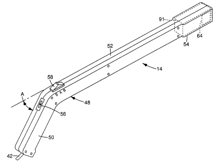
Figure 3 is a perspective view of the probe
unit of the circuit tracing system of the present
invention;
Figure 4 is a perspective view of the probe
electronics, including the sensor array;
Figures 5A, 5B and 5C are front, side, and rear
2o elevational views, respectively, of the novel guarded
electrodes used in the electric field and differential
sensors of the probe electronics;
Figure 6 is a block diagram of the transmitter
electronics;
Figure 7 is a block diagram of the probe
electronics;
Figure 8 is a schematic diagram illustrating
the driven shield of the guarded electrodes used by the
probe unit; and
Figure 9 is a block diagram of the receiver
electronics.
Description of the Preferred Embodiment
With reference now to the figures, and in
particular with reference to Figures 1-3, there is
depicted the circuit tracing system of the present
invention, which is generally comprised of a transmitter
WO 94/08257 PCT/US93/07753
21 ~ 3'~ 6 6
-6-
unit 10 (Figure 1), a receiver unit 12 (Figure 2), and a
probe unit 14 (Figure 3). The circuit tracing system is
particularly suited to locate electrical conductors
(wires) having a break therein at an unknown location,
i.e., open circuits, although it is equally useful with
conductors in a closed-circuit, and operates whether the
conductor is above or below ground. Transmitter unit 10
(discussed in greater detail below in conjunction with
Figure 6) provides a test signal which is applied to the
conductor by means of a cable 16 having an appropriate
connector i8. Transmitter unit 10 is also equipped with
a second cable 20 to provide a ground reference. These
cables and connectors may take on various physical
embodiments depending upon the nature of the circuit to
be tested. For example, if the wire to be traced were
connected to a standard electrical wall outlet, cables 16
and 2o could be combined into a single cord having a
compatible standard plug. Transmitter unit 10 also has
an on/off switch 22, a gain control switch 24; it may
2o further have a speaker or sounder 26 for indicating the
power (on/off) status or battery condition. The
components of transmitter unit 10 are all contained in a
housing 28.
Receiver unit 12 similarly includes an on/off
switch 30, a gain control knob 32, and a readout dial or
meter 34 for displaying the amplitude of the received
signal. A speaker 36 is also provided so the operator
can hear the relative strength of the received signal,
and another switch 38 is provided to change the output of
receiver unit 12 from a compressed logarithmic scale to
an expanded logarithmic scale. A connector port 40
receives the cable 42 from probe unit 14. The components
of receiver unit 12 are contained in a housing 44, which
has attached thereto a shoulder strap 46.
Probe unit 14 is constructed of a housing 48
having a handle or grip portion 50, an arm or extension
portion 52, and a head or end portion 54. Housings 28,
WO 94/08257 214 3'7 6 6 PGT/US93/07753
44 and 48 are all ideally water resistant, and
constructed of any durable material, preferably a polymer
such as high-density polyethylene (HPDE), acrylonitrile
butadiene styrene (ABS), or polystyrene (PS). The
overall length of housing 48 is preferably about 66 cm.
Handle 50 has an appropriate size and shape to allow the
operator to grasp probe unit 14. Proximate handle 5o are
a level vial 56 (a liquid-filled tube containing an air
bubble), and a switch 58. Level 56 allows the operator
to determine the depth of a buried cable using
triangulation, as further explained below. Switch 58
allows the operator to choose one of three sensors in
location and tracing of the conductor, as explained
further below.
Probe head 54 contains the novel sensor array
shown in Figure 4. Three sensors are provided on the
printed circuit board (PCB) 60: a single-ended electric
field sensor comprising a first guarded electrode 62,
located at the front end of head 54; a differential
electric field sensor comprising second and third guarded
electrodes 64 and 66, located at the sides of head 54 and
generally parallel to one another; and an inductive
sensor comprising an~induction coil 68 located between
electrodes 64 and 66, with its axis perpendicular to the
face of electrode 62, i.e., in alignment with arm 52.
Coil 68 is constructed with a high initial permeability,
low retentivity core, and has a high Q to produce the
best possible signal-to-noise ratio. Preamplifiers 70
are provided for each of the electrodes 62, 64 and 66 and
coil 68. The leads 72 from preamplifiers 70 are
connected to an analog switch. The analog switch is
controlled by wires which traverse the length of arm 52
and are connected to the input contacts of switch 58. As
explained further below, the analog switch is connected
to a differential amplifier which in turn is connected to
wires in cable 42 which exit handle 50.
The construction of the guarded electrodes 62,
W~~~Q~~~ PCT/US93/07753
-g-
64 and 66 is shown in Figures 5A-5C. Each electrode has
an electrically insulative substrate 74 which is
preferably formed of the same material as a printed
circuit board, i.e., an epoxy resin composite. The rear
face 76 of the electrodes has a metallic shield 78 bonded
to substrate 74; rear shield 78 has a plurality of slots
80 (preferably about 0.25 mm wide). The front face 82 of
the electrodes has a metallic sensing element 84 with a
plurality of similar slots, preferably parallel with
slots 80, and a pair of metallic borders or strips 86
surrounding sensing element 84, forming an incomplete
ring shield. Element 84 and strips 86 are also bonded
directly to the surface of substrate 74. The preferred
material for element 84 and ring and rear shields 86 and
78 is copper. Rear shield 78 has two copper-plated holes
88 therein which pass through substrate 74 to provide a
lead for electrical conductivity with strips 86, and has
another copper-plated hole 90 with an insulative border
which passes through substrate 74 to provide a contact
for sensing element 84. The resulting guarded electrodes
are highly directional (i.e., in the direction generally
perpendicular to the surface of sensing element 84).
This characteristic is termed directional because the
magnitudes of the potentials of the sensed equipotential
electric field surfaces surrounding the energized
conductor diminish with distance from the conductor. A
differential electrical field potential sensor can only
measure the difference in the potential of two
equipotential surfaces. If the sensor is aligned such
that the two sensing elements both lie in one
equipotential surface, the detected difference is zero.
If the sensor is aligned such that a line from one
sensing element to the other is perpendicular to an
intersecting equipotential surface, the detected
difference is a maximum. Thus, as the differential
sensor is rotated about any axis embedded in an
equipotential surface, the detected difference will
WO 94/08257 ~ ~ ~ PGT/US93/07753
_g_
change from zero when the line between the two sensors is
in the surface (or tangent to the surface), to the
maximum when the line is perpendicular to the surface.
In other words, the amplitude of the sensed electric
field potential is dependent upon its angular location
with respect to the normal of element 84. The novel use
of such directional electrodes in a differential sensor
has been shown to greatly improve the spatial resolution
of.probe unit 14, and eliminates any need for
simultaneous sensing by, e.g., an inductive sensor.
The sensor array (i.e., the space defined by
PCB 60 and the components thereon) is partially shielded
by a metallic box-like screen 91 within probe head 54,
the screen having cutouts corresponding to the location
of electrodes 62, 64 and 66. Screen 91 is also provided
with a longitudinal gap to prevent eddy currents, and is
connected to the circuit ground. The slots in rear
shield 78 and sensing element 84 allow the magnetic field
lines generated by current in the conductor to penetrate
head 54 to coil 68; slots need be provided only in the
electric field sensor (electrode 62) for this purpose;
however, for ease of manufacture, the same slotted design
is used for all three of the electrodes 62, 64 and 66.
The use of the guarded electrode array and screen 91
yields high resolution in the location process due to
ease of precise alignment with the normal to the electric
field equipotentials and due to the maximum decoupling
obtained from earth ground.
Those skilled in the art will appreciate that
the differential sensor would still function even if the
electrodes were not guarded, although this would decrease
their resolution. Also, it is not necessary for the
electrodes 64 and 66 to be completely parallel with one
another. For example, the differential sensor would
still theoretically be able to provide a differential
signal even if these two electrodes were coplanar. In
other words, it is only necessary to position electrodes
WO 94/0$257 PCT/US93/07753
214'766
-10-
64 and 66 at two minimally spaced apart locations in
order that they be able to detect the different
equipotential surfaces.
Referring now to Figures 6-9, the various
electrical circuits in the circuit tracing system are now
explained. A block diagram of the electronics of
transmitter unit 10 is shown in Figure 5: A crystal
oscillator 92 and a divider 94 comprise the frequency
source for the transmitter. The frequency of the test
signal may vary widely but, in the disclosed embodiment,
the transmitter frequency is in the range of 1 kHz to 300
kHz, preferably about 4-32 kHz, and most preferably about
16 kHz. The latter frequency is rarely used in other EM
emission devices, and also balances the competing
requirements for coupling between the signal radiating
from the conductor and the electrodes when the electric
field mode is used, versus current loading of the
conductor when it is underground. A battery 96 may be
supplied to provide power to unit 10, although an
external power source could alternatively be used. It is
understood that the various components of transmitter
unit 10 are powered by battery 96 although the electrical
connections between the battery and the components is
omitted for clarity; similarly, all power supplied from
battery 96 is controlled by on/off switch 22.
Divider 94 is connected, and provides audible
tones, to a battery condition checking circuit 98; if
circuit 98 detects low battery power, a sounder 26 is
activated. The output of oscillator 92 is also directed
to a flyback control circuit 102 which provides voltage
conversion to maintain a specified maximum power output
regardless of load on the circuit, and is controlled by
gain control switch 24. Flyback control circuit 102
includes circuitry to limit the energy stored in a
flyback transformer contained in flyback supply 106. The
output of flyback control circuit 102 is directed to
flyback supply 106 wYrich~converts battery energy to a
WO 94/08257 214 3 7 6 ~ PCT/US93/07753
-11-
voltage for the output power amplifier 108 such that the
power from flyback supply i06 does not exceed an amount
selected by control switch 24. The regulated signal is
sent to an amplifier 108, and then to the output network
110 which is connected to cables 16 and 20. Output
network 110 includes inductive and capacitive resonant
circuits to effectively couple to a wide range of
resistive, inductive, and capacitive loads, while
reducing the harmonic content of the output signal. The
transmitter output is thereby operable for impedances of
1 mfl to 1 Mt1 or more. The amplitude of the test signal
is preferably no more than 50 volts for personnel safety
and battery economy.
A block diagram of the electronics of probe
unit 14 is shown in Figure 7. As mentioned above, each
of the electrodes 62-66 and coil 68 is connected to one
of the preamplifiers 70 which, in the preferred
embodiment, are junction field-effect transistor (JFET)
buffer amplifiers. The outputs of preamplifiers 70 are
connected to an analog switch 112 which is controlled by
mechanical switch 58 to selectively provide a single
output based upon only one of the electric field sensor,
the differential sensor, or the inductive sensor. Upon
reference to the remainder of the specification, those
skilled in the art will appreciate that the differential
sensor and inductive sensor could be used simultaneously;
in the preferred embddim~nt, however, they are not so
used since, as those skilled in the art will further
appreciate, there is no practical advantage and or
synergistic effect to the combined use of the
differential sensor and the inductive sensor and, indeed,
use of switch 58 and analog switch 112 ensures that the
connection to one of the sensors is completely broken
before a connection is made to another sensor ("break
before make"). Analog switch 112 is preferably the
switch commonly known as number 4053B, and is sold by
many companies, including Radio Corporation of America
WO 94/08257 PCT/US93/07753
2143766
-12-
(RCA). The output from analog switch 112 is provided to
a differential amplifier'i13 which sends the signal to
receiver unit 12 via cable 42. Power for the various
components of probe unit 14 is supplied by the battery in
receiver unit 12, via wires in cable 42.
As further shown in Figure~8, each of the
electrodes 62, 64 and 66 have "driven" shields or guards.
The output voltage from each electrode may be maximized
by reducing the effective capacitance of the electrode
with respect to ground. In the present invention, this
is accomplished by energizing the ring and rear shields
at a voltage which is equal to the voltage at the sensing
element, forming the driven shield. The output of a non-
inverting amplifier 114 is connected to strips 86 and
rear shield 78, preventing coupling of sensing element 84
to ground through the regions occupied by either the ring
shield or the narrow gap~formed by substrate 74. In
order to avoid a damaging discharge into FET amplifiers
70, capacitors 115 and 117 preferably has a capacitance
in the range of 10-10,000 picofarads.
Introducing any conductive object near the
energized conductor affects the shape of the
equipotential electric field surfaces. It is thus
desirable when measuring the electric field to disturb it
as little as possible. The driven guarded electrode
minimizes the introduction of such a disturbance since it
aligns the potential of the guard to that of the sensing
electrode and therefore close to the potential of the
equipotential electric field surface in which it lies.
The driven guarded electrode also allows the input
impedance of the electrode to be higher than if it were
not driven, resulting in less disturbance of the
equipotential surface. For these reasons, a driven
guarded electrode is superior to non-driven, guarded
electrodes, yielding the greatest possible signal prior
to amplification, and further eliminating sensing of any
voltages from the circuitry in probe head 54. The use of
WO 94/0257 214 3 7 6 fi P~/US93/07753
-13-
high gain, low noise amplifiers 70, along with the driven
shield on the guarded electrodes, greatly increases the
sensitivity of the single-ended and differential sensors
in tracing low-voltage or remote conductors.
A block diagram of the electronics of receiver
unit 12 is shown in Figure 9. Again, the battery
connections are omitted for ease of viewing Figure 9, but
it is understood that a battery is supplied for receiver
unit 12 in the same manner as shown for transmitter unit
10 in Figure 6, including a battery condition checking
circuit, and the battery of receiver unit 12 is
controlled by switch 30. Another oscillator 116 and
divider 118, tuned to the same frequency as transmitter
unit 10, provide the frequency source for receiver 12.
The output of divider 118 is directed to the detection
circuits described below, and to a phase-lock-loop (PLL)
frequency synthesizer 120. The signal from probe unit 14
passes through a first variable attenuator 122, a low
pass filter 124, and a second variable attenuator 126.
Both attenuators are regulated by gain control knob 32,
and simply maintain the amplitude of the received signal
in the range necessary to sufficiently observe the signal
but also avoid applying an overvoltage to the remaining
circuitry, i.e., when the received signal is very strong.
The output of attenuator 126 is directed to a switch
driver 130 which drives mixer switch 132, whose input is
from PLL 120. The resulting output of mixer switch 132,
an intermediate frequency (IF) signal, passes through
another low pass filter 134 and a bandpass filter 136
which together comprise an IF amplifier.
The conditioned signal from bandpass filter 136
may be processed in many different ways to provide
detection of the test signal from transmitter unit 10.
In the preferred embodiment, receiver unit 12 performs
the pseudo-synchronous detection routine as more'fully
described in U.S. Pa~ent,No. 4,942,365, which determines
the magnitude of the signals from the sensors. The
WO 94/08257 PCT/US93/07753
~143~66
-14-
sinusoidal signal from bandpass filter 136 is used as an
input to another switch driver 138 which drives two
synchronous detectors 140 and 142. Each of the
synchronous detectors includes an inverter and an analog
switch, the analog switch having two inputs, one being
the unmodified signal from switch driver 138, and the
other being the inverted form of that signal. In
detector 140, the analog switch is responsive to the
reference signal from divider llSain detector 142, the
analog switch is responsive to the reference signal from
divider 118 with a 9Q° phase shift. The two signals from
detectors 140 and 142 pass through Bessel low pass
filters 144 and 146, respectively, and are then combined
in a pseudosynchronous, or chopper analog, switch 148,
which is also responsive to the reference signal from
divider 118. The pseudosynchronous signal is directed to
an RMS detector 150, which passes the signal level to an
amplifier 152. The output of amplifier 152 may be based
on a compressed or expanded logarithmic scale depending
upon the setting of switch 38. The output is directed to
both meter 34 and speaker 36.
Operation
Operation of the circuit tracing system of the
present invention begins by attaching the signal cable 20
of transmitter unit=1.0 to the accessible portion of the
conductor, and attaching ground cable 18 to a local
ground. Those skilled in the art will appreciate that
the signal may be applied inductively if it is impossible
or undesirable to directly (conductively) apply the
signal. On/off switch 22 is turned on and, if the
battery check is acceptable, gain control switch 24 is
adjusted according to the particular conditions, i.e.,
"low" for short range tracing, "high" for long range.
The voltage applied by the transmitter results in the
alternate charging and discharging of the cable, creating
a time-varying electric field potential which can be
WO 94/08257 PCT/US93/07753
-15-
detected by electrodes 62, 64 and 66. Furthermore, if
the conductor is part of a closed circuit, an alternating
current will be established which creates an
electromagnetic field detectable by the inductive sensor.
Cable 42 of probe unit 14 is plugged into connector 40 of
receiver unit 12, and on/off switch 30 is turned on.
Again, assuming the battery checks out alright, gain
control knob 32 is adjusted according to the conditions.
If the general lr~cation of the conductor is known, switch
38 may be moved to the expanded logarithmic setting which
gives the sharpest null and best resolution in location
of a cable, but if the probe is being used at a location
fairly distant from the transmitter and the location and
depth of the cable are uncertain, then the operator may
want to start with switch 38 at the compressed
logarithmic setting°to get a general feel for the
direction of the conductor.
The operator may want to begin tracing with
switch 58 of probe unit 14 in either the setting
corresponding to the inductive sensor, or the setting
corresponding to the single-ended sensor. Use of the .
single-ended sensor allows the user to confirm that the
system is operating properly. This is accomplished by
moving probe unit 14 close to, and pointing at, the
transmitter lead 16; if a signal is not immediately
detected, then the equipment should be checked for a
possible malfunction. If the signal is detected, then
the operator will move probe 14 to the general area where
the conductor is to be located. The single-ended sensor
is then used to find the general direction to and
location of the conductor. Switch 58 may thereafter be
set to either the differential sensor or the inductive
sensor, depending upon the specific conditions.
Notwithstanding the foregoing, the inductive
sensor may instead be used first if the conductor forms a
closed-loop or immediately extends underground. Even if
the conductor is open and above ground, if the starting
WO 94/08257 PCT/US93/07753
214~'~ 66 _16_
location for tracing is relatively close to the
transmitter, then the conductor may carry enough current
for a short distance to allow tracing with the inductive
sensor and, if so, this form of detection will be more
accurate than the single-ended electric field sensing.
Switch 58 may thereafter~be moved to the differential
sensor setting when the electromagnetic signal weakens.
The single-ended electric field sensor (electrode 62) is
normally used only to find oi~e wire among a bundled cable
to of wires, or for pinpointing the terminus of an open-
ended conductor.
Regardless of which sensor is used, location
proceeds by following the path of the conductor while
swinging the probe transversely to the conductor (i.e.,
left-right-left). Arm extension 52 of probe 14 should be
held at an orientation generally perpendicular to the
conductor. For example, if the conductor extends
vertically in a wall, extension 52 should be horizontal,
but if the conductor travels horizontally underground,
then extension 52 should be vertically pointed straight
at the ground. During the swinging movement, when the
probe is pointed directly towards the conductor, meter 34
and/or speaker 36 will provide an indication of alignment
(i.e., a peak signal from the single-ended electric field
sensor, or a null signal from the differential electric
field or inductive sensors).
If the portion of the conductor being traced is
underground, the surrounding conductive mass of the earth
may limit the electric field to a region very close to
the conductor, making detection by electric field sensors
difficult or impossible. In such cases, however, the
high capacitance of the conductor to earth allows a small
current to flow even in an open conductor, and the
electromagnetic field established thereby can be sensed
by coil 68 (when oriented in the proper direction).
There are cases where the electric field sensors are
preferred for underground conductors. If the conductor
214 3 7 ~ ~ P~/US93/07753
WO 94/08257
-17-
is buried shallow or is in poorly conducting soil, the
technique is viable, and can further aid in
discriminating the paths of the desired conductor even
when it is in the vicinity of other conductors. In such
a case, the tracing signal may flow in the other
conductors as well, and magnetic sensing cannot easily
discriminate between these other conductors and the
desired conductor, whereas the desired conductor can be
adequately discriminated with the differential electric
field sensor. Also, while the terminus of a buried open
conductor can be determined using the inductive sensor,
if the conditions are conducive to use of the electric
field sensors, then the location of the terminus can be
determined more precisely with the single-ended sensor.
If the conductor is underground, the operator
may also want to know its depth. This may easily be
determined by using level 56 in a well-known
triangulation operation. Once the azimuthal location and
direction of the conductor is known, a marker, such as a
pin flag, may be placed on the ground. The operator then
moves away from the marker, in a direction perpendicular
to that of the conductor path, while maintaining the
probe in an orientation wherein the bubble in the level
remains between the two lines, i.e., with handle 50 at a
horizontal pitch. As the operator moves away from the
conductor, meter 34'will begin to drop off, establishing
a null or reference point for triangulation at the
location of the minimum signal. By measuring the
distance from this reference point to the marker, and
knowing the relative angle between handle 50 and
extension 52, the operator may calculate the depth of the
conductor. To simplify this procedure, however, handle
50 preferably extends at an angle A of 45° with respect
to extension 52. In this manner, the triangle formed by
the conductor, the marker, and the reference point is
isosceles and, therefore, the depth of the conductor is
approximately equal to the distance from the reference
WO 94/08257 PCT/US93/07753
-18-
~,~ ~3~ ~ 6
point to the marker. Thus, no calculation need be made
other than measuring this distance.
Although the invention has been described with
reference to specific embodiments, this description is
not meant to be construed in a limiting sense. Various
modifications of the disclosed embodiment, as well as
alternative embodiments of the invention, will become
apparent to persons skilled in'the art upon reference to
the description of the invention. It is therefore
contemplated that such modifications can be made without
departing from the spirit or scope of the present
invention as defined in the appended claims.