Note: Descriptions are shown in the official language in which they were submitted.
WO 94/06181 1 ~ 1 4 3 9 4 4 - PCT/US93/08444
-1-
Multi-stripe Array Grating Integrated Cavity Laser
SPECIFICATION
Field of the Invention
The invention relates generally to semiconductor lasers; in particular, it
5 relates to multi-wavelength integrated semiconductor lasers.
Background Art
Multi-wavelength semiconductor lasers are needed for several
applications, particularly for wavelength-division multiplexing (WDM)
telecommunications systems including computer buses. In such systems, multiple
1() laser.s each emitting at a different frequency are separately modulated by different
dat~ signal.s, and all the so modulated optical carriers are impressed on a single
optical fiber. At the receiving end of the fiber, the separate optical wavelengths are
separated by a spectrometer or other wavelength-sensitive means so that each single
optical channel can be extracted from the fiber and detected. The absorption
15 spectrum of the silica Sber used in long-distance telecommunication networks
dictates that the optical carriers be in the 1.3 or 1.5 ~m bands available in InP and
related active opto-electronic materials while the shorter computer buses can use the
O.X llm band available in GaAs.
For economy and ease of operation, the multiple lasers should be
2() integrated on a single inte~rated circuit chip, that is, an opto-electronic integrated
circuit (OEIC). Chang-Hasnain has disclosed a method of fabricating an array of
vertical-cavity, surface-emitting lasers emitting at different wavelengths in U.S.
Patent 5,029,176. Althou~h her method allows the fabrication of a large number of
individual lasers, present designs for conllllullication networks do not foresee a need
25 for more than 2() to 40 separate wavelengths separated by about 1 or 2 nm. Her
design suffers from doubts about its reproducibility, its incompatibility with wafer-
scale fabrication, and the vertical emission of the laser li~ht. It would be preferred to
~ retain a planar geometry for ease of packaging.
A different approach uses distributed feedback (DFB) edge-emitting
30 lasers in which separate Bragg diffraction gratings determine the lasing wavelen,~ths.
The period of the gratings are tailored for the separate wavelengths. The state of the
art in this approach, presently about 2() lasers on a single integrated circuit chip, is
disclosed by Zah et al. in "1.55 ~m tensile-strained single quantum well 2()-
wavelen,~th distributed feedback laser arrays"~ El~ctronics L~tt~rs vol. 2~ 2,
WO 94/06181 2 1 ~ 3 ~ 4 ~ : PCI/US93/08444
pp.lSX5-15X7. This approach suffers from two disadvantages. First, if the laser
integrated circuit is to attain a channel spacing of about 1 nm, then the variation in
the periods of the diffraction gratings and other portions of the structure must be
controlled to about this same distance. The etching and lithography becomes very5 difficult in satisfying such tight dimensional control. Secondly, the efficient
coupling of the multiple laser emissions into a single optical fiber remains unsolved.
Of course, bulk optical lenses could be used to focus the outputs to the small fiber
core, but such an approach would be neither economical nor rugged.
Several groups have proposed fabricating an OEIC spectrometer which
I () could be integrated with multiple detectors for a WDM application. See, forexample, Gibbon et al. in "Optical performance of integrated 1.5 ~m grating
wavelength-demultiplexer on InP-based waveguide," Electronics Letters, vol. 25,
19X9, pp. 1441-1442, Soole et al. in "Monolithic InP/lnGaAsP/lnP grating
spectrometer for the 1.4X-1.56 ~n wavelength range," Applied Physics Letters,
15 vol. SX, 1991, pp. 1~49-1951, and Cremer et al. in "Grating spectrograph in
InGaAsP/lnP for dense wavelength division multiplexing" Applied Physics Letters,vol. 59, 1991, pp. 627-629. In these approaches, multiple waveguides are formed in
the surface of an OEIC. One of the waveguides acts as an input waveguide receiving
light from off the chip. The input light exits the input waveguide on its interior end
2() and irradiates a vertically arranged diffraction grating formed into the chip's surface.
The grating spectrally separates the light to the other waveguides, which act asoutput waveguides. Separate optical detectors are fabricated on or otherwise
associated with the output waveguides for detecting the spectral components of the
light. Such a design could conceivably be adapted for parallel DFB lasers formed in
25 such waveguides, but it would not be satisfactory. The DFB gratings would still
require precise lithography. Also, the diffraction grating would not be completely
decoupled from the optical cavities of the DFB lasers, and the coupled cavities
would necessitate a complex and constrained design. Pratt et al. disclose a related
related bulk-optical design in "Four channel multiple wavelength laser transmitter
3() 1nodule for 155() nm WDM systems," Electronics Lette)-s, vol. 2X, 1992, pp. 1066-
1 ~)67.
A related design for a multi-wavelength laser array takes advantage of
the resonances of the optical cavity associated with the diffraction grating, as has
been disclosed by Kirkby et al. in U.K. Patent Application, 2.225,4X~2A; by Kirkby
35 in "Multichannel Wavelength-Switched Transmitters and Receivers--New
Component Concepts for Broad-Band Networks and Distributed Switching
Systems," .lou~/tal of Li~htwave Technolo~y, vol. X, 19~0, pp. 2()2-211; by White et
WO 94/06181 ~ 21~ 3 ~ ~ 4- PCr/US93/08444
al. in "Demonstration of a Two Wavelength Multichannel Grating Cavity Laser,"
12th International Conference on Semiconductor lasers, 1990, pp. 210-211, in
"Demonstration of a 1 x 2 multichannel grating cavity laser for wavelength division
multiplexing (WDM) applications," Electronics Letters, vol. 26, 1990, pp. X32-X34,
5 and in "Crosstalk compensated WDM signal generation using a multichannel grating
cavity laser," European Conference on Optical Communications, 1991, pp. 6~9-692;by White in "A Multichannel Grating Cavity Laser for Wavelength division
Multiplexing Applications," Jourltal of Lightwav~ T~chnology, vol. 9, 1991,
pp. X93-X~X; and by Nyairo et al. in "Multichannel grating cavity (MGC) laser
1() transmitter for wavelength division multiplexing applications," Journal of EE-J
Proceedings, vol. 13X, 1~91, pp. 337-342. Although Kirkby et al.'s patent
application suggests an integrated desi~n, the experimental results of this workinvolve.s a separate planar diffraction grating, a bulk lens, and a laser bar of active
waveguides formed in a chip. Multiple parallel rib waveguides are formed in the
15 laser bar, each of which could be separately electrically pumped. One waveguide
serves as the master amplifier guide while the remainder of the waveguides serves as
active reflector guides. None of the waveguides are frequency selective within the
overall bandwidth of the laser array, that is, no distributed feedback nor Braggreflective gratings are formed over the waveguides. Lasing is achieved by
2() simultaneously driving both the master amplifier and a selected one of the reflectors.
The combination of master amplifier and selected reflector determine the lasing
wavelength because the diffraction gratin,~ controls which wavelength propagatesbetween the two. The design ensures that no single rib can lase on its own. The
advantage of this approach is that the lasing wavelengths are determined by the
25 relative spatial positions of the waveguides and the diffraction grating, a much easier
arrangement to set up than the fabrication of DFB gratings. However, simultaneous
multi-wavelength emission creates a problem because the cavities for the different
wavelengths, whether in the bulk optical structure or the proposed integrated
structure, all include the one active master amplifier. Carrier depletion introduces
3() significant crosstalk between the wavelen~th channels as they interact in the master
~ amplifier. White et al. in the last paper cited above and Nyairo et al. attempt to
suppress the crosstaLlc with active feedback control or other methods. However, such
suppression is considered unsatisfactory because of its active nature. Farries et al.
have disclosed an external cavity multi-wavelength laser in "Tuneable
35 multiwavelength semiconductor laser with single fibre output," Elcctronics Lettcrs,
vol. 27, l'~'~1, pp. 14~X-14'~). Their device uses a bar similar to Kirkby's for a laser
array with no frequency determination and relies on lenses and a bulk diffraction
WO 94/06181 . :~ . PCI/US93/08444
~1~39~'4
-4 -
grating to define a multi-wavelength cavity.
Summary of the Invention
The invention may be summarized as a multi-wavelength integrated
cavity laser in which a plurality of active waveguides of wide gain bandwidth, a5 passive output waveguide, and a diffraction grating are formed in a substrate. The
geometrical relationship of the elements determines the lasing wavelengths of the
active waveguides, which can be independently activated. All wavelengths are
coupled into the passive output waveguide.
Brief Description of the Drawings
FIG. I is a plan view of a multi-wavelength integrated laser of the
invelltion.
FIG. 2 is a schematic diagram of the geometry of a Rowland-circle
spectrometer.
FIG. 3 is a diagram, partially in plan view and partially schematic, of
15 the Rowland circle applied to the laser of the invention.
FIG. 4 is a cross-sectional view of the active stripes taken along
sectional line ~ 4 of FIG. 1.
FIG. 5 is a cross-sectional view of the passive output waveguide taken
along .sectional line 5--5 of FIG. 1.
2() FIG. 6 is a cross-sectional view of the grating trench taken along
sectional line ~6 of FlG. 1.
Detailed Description of the Preferred Emb~diment
An embodiment of an integrated multi-wavelength laser 10 is illustrated
in plan view in FIG. 1. On a substrate of a single integrated circuit chip 10 are
25 formed a plurality of active waveguide stripes 14, a passive output waveguide 16,
and a diffraction grating IX. Interior ends 20 of the active stripes 14, an interior end
22 of the output waveguide 16, and the diffraction grating 1~ are formed in a
Rowland-circle focu.sing geometry to be described in more detail later. Each of the
active stripes 14 can be separately electrically pumped so as to output light from it.s
3() interior end 2(). This light diffracts from the diffraction grating IX to the output
waveguide 16. An optical cavity is set up within and between the active stripes 14
and the output waveguide 16, and the Rowland-circle geometry between each activestripe 14, the grating IX, and the output waveguide 16 determines the resonant
wavelength (frequency) of the stimulated light emitted by that active stripe 14. The
35 resulting laser light is emitted from the laser device 1() through an external end facet
1'~ of the output waveguide 16. If more than one of the active stripes 14 are
WO 94/06181 ~' 2 1 ~ 3 ~ ~ ~ PCI /US93/08444
electrically pumped, multiple wavelengths are emitted from the exterior end 19 of
the output waveguide 16. There are no Bragg diffraction gratings or other frequency
selective means operatively associated with the separate active stripes 14 beyond the
gain bandwidth and other frequency-limiting features of the entire laser, which
5 encompasses all the selectable wavelengths.
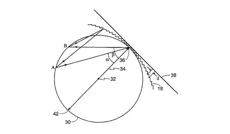
The Rowland circle geometry, illustrated schematically in FIG. 2, is
well known in x-ray optics. A Rowland circle 30 has a radius R /2 about a center 32.
A circle diameter 34 defines at one end a tangent point 36 with a straight tangent 3X
and a circular grating 1 X. The grating 1 X has a radius R about the other end 42 of the
1() circle diameter 34 and has a constant pitch d as projected on the straight tangent 3X.
As is well known, if the diffraction grating 1 X has a large extent, the pitch d needs to
vary along its length in order to reduce optical aberrations. In x-ray diffraction, a
Rowland-circle spectrometer is usually used to spectrally separate and focus a
multi-wavelength source at point A to a photographic plate or other detector at or
15 surrounding point B, but in the laser of the invention point B is associated with the
active stripes 14 and point A with the output waveguide 16. The diffraction
condition is given by
d[sina + sin~ = P , (1)
where a and ~ are the angles between the respective lines connecting points A and B
2() with the tan~ent point 36 and the circle diameter 34, ~ is the free-space wavelength
of the light, /1 iS the index of refraction of the medium within the Rowland circle 30,
and p is the diffraction order, a non-zero integer. Assuming that a is fixed, there is a
different ~ for each ~.
As applied to the present invention, as illustrated in nG. 3, the interior
25 ends 2() of N parallel active stripes 14 are positioned about point B from angle ~I to
~N. with corresponding resonance wavelengths ~I to ~N as determined by
Equation (1). The central active stripe 14, having an angle ,B( is aligned with the
tangellt point 36. The interior end 22 of the output waveguide 1~ is positioned at
point A at angle a. Although the output waveguide 16 is generally parallel to the
3() active stripes 14, for the sake of light-gathering efficiency, it has a curved portion 37
so that its interior end 22 is aligned with the tangent point 36, that is, bears an angle
a with the perpendicular 34 to the line tangent 3X of the diffraction grating 1 X.
The re,sonant wavelengths ~l to ~N are determined by the Rowland-
circle geometry and not by individualized structure.s of the active .stripe.s 14. When
35 one or more of the active stripes 14 are electrically pumped. the output waveguide
WO 94/06181 ~ 13 9 g 4; ~ PCI/US93/08444
16 receives light at the one or more resonant wavelengths associated with those
active stripes 14. Because there is no electrical pumping or other gain in the output
waveguide 16, crosstalk associated with carrier depletion is eliminated. The
resonant cavity of the multi-wavelength laser includes the optical path between the
5 selected active stripe, the diffraction grating, and the output waveguide, and all of
the active stripe and output waveguide. For lasing to occur, a significant portion of
the light coupling into the output waveguide must be reflected back toward the
selected active stripe.
We are pursuing an implementation of the laser of the invention. It is
1() designed to emit around 1.545 ~m from ~ active stripes. The spectrometer is
designed with a Rowland radius R of l 3 mm, a grating spacing d of 5 ~rrt, an angular
e~tent of the grating of 2()~ with respect to the output waveguide, and an effective
index of refraction /t of 3.244. The diffraction order p is 17-th order. The angular
spacing (x of the output waveguide is 4~~, and the active stripes are spaced at ,B
15 between 6() and 64~. As a result, the lateral spacing of the active stripes is about
50 ~lm. Variable blazing is used on the diffraction grating so that, all along the
grating, light is specularly reflected off the grating facets between the center of the
stripe array and the output waveguide.
The above geometrical dimensions allow a design that suppresses lasing
2() between two active stripes directly linked through the diffraction grating. The
active-to-passive coupling occurs in 17th order forp at wavelengths ~ between 1.530
and 1.558 !lm according to Equation (1). The corresponding equation for light
diffracted between two active stripes i and j is given by
d[sin,B; + sin~ = P , (2)
25 According to this equation, the active-to-active coupling occurs in 19th order in p'
for wavelengths between 1.479 and 1.529 ~m and in l~th order between 1.561 and
1.614 ~t. Also, according to Equation (1), the active-to-passive coupling for lXth
al1d 16th order in ~ occur at wavelengths between 1.445-1.471 and 1.626-1.656 llm,
respectively. Thereby, the desired wavelength band avoids the band of any
3() undesired reflections. To take advantage of this separation, the gain peak of the
active medium is centered within the desired band through choice of the composition
and thickne~sses of layers comprising the multi-~uantum wells so that the active-to-
active mode~s have lower gain than the desired active-to-passive modes. If a mode is
to lase. its gain less it.s loss per round trip within the cavity must be equal to zero.
35 The above described grating blazing reduces the light backscattered to another active
WO 94/06181 ~ 9 4 ,~ PCl/US93/08444
stripe and thus increases the loss of the active-to-active modes to the point where
lasing cannot occur. Only the active-to-passive coupling and associated gain
spectrum are high enough to support lasing.
The integrated laser chip In can be grown as illustrated in cross-section
5 in FIG. 4 for the array stripes 14, in FIG. 5 for the passive output waveguide, and in
FIG. 6 for the diffraction grating IX. All growth is epitaxial and performed by
organo-metallic chemical vapor deposition operating at 76 torr at 620~C. On a
(10())-oriented 11+-lMP substrate 50 is grown an n-type IMP buffer layer 52 doped
1()l8cnl-2 with sulfur and having a thickness of 0.5 ~n. An IIIGaAsP waveguide
I () core layer 54 is grown over the buffer layer 52. Its composition is lattice-matched to
InP and provides a 1.3 ~nt bandgap. It is doped n-type to 10l7cm-3, and has a
thickness of ().3 ~n. An unillustrated thin etch-stop layer of 111P is deposited over
the core layer 54 to a thickness of 3() ~mn The lower 15 nm is l1-type at 5xl01; cm
while the upper 15nm is undoped. A multiple quantum-well (MQW) layer 56,
15 illustrated only in FIG. 4 although it is initially deposited in all regions, is grown
over the core layer 54. It consists of 6 InGaAs wells with l~lGaAsP barriers
therebetween. The wells are about X nm thick while the barriers are about 10 nm
thick and their composition has a bandgap of 1.3 I~lm. Both compositions are
lattice-matched to InP. Over the MQW layer 56 is grown an upper p-contact layer
2() 5X consisting of about ().1 ~n of undoped IIIGaAsP having a 1.3 llm bandgap
followed by a 0.1 ~m layer of undoped InGaAsP having a 1.2 ~m bandgap followed
by ().~ ~n of InP doped /~-type with zinc and graded from 1()l7cnl--3 to 7xl()l7cm-3
and then followed by 0.2 ~m of InGaAsP doped p-type with 7x1()l8 and having a
bandgap of 1.3 ~m.
Up to this point, there has been no lateral definition. An SiO 2 mask is
deposited and patterned with stripes corresponding to the active stripes 14 and
extending along the [011] direction. The unmasked regions are first dry etched by
ion-milling with argon and then wet etched with H3PO4:H202:H20 (1:1:8, by
volume using standard reagent concentrations). The etch-stop layer above the core
3() layer 54 defines the bottom of the wet etching. The wet etching is continued until
- the width of the MQW region is reduced to such a dimension that the fully fabricated
stripe 14 supports only single-mode propagation along the stripes. After etching, the
~ chip is returned to the OMCVD chamber for regrowth of a semi-insulating layer 6()
of F~ P to a thickness of I ~n. The semi-insulating layer 60 isolates the stripes
35 14, passivates the sides of the MQW layer 5~, and provides an upper cladding in the
planar waveguide section extending throu~h the interior of the Rowland circle.
WO 94/06181 2 1 ~ 3 9 4 4 PCI/US93/08444
-X -
The passive output waveguide 16 of FIG. 5 and the diffraction grating
1~ of FIG. 6 are then formed by depositing an SiO2 layer 64 onto the entire area of
the integrated circuit chip 10 and patterning this layer with openings 65 to define the
output waveguide 16 and with an opening 66 to define the diffraction grating 18.S The shape of a rear boundary 67 of the grating opening 66 is nearly a biLI~ly. The
entire area of the integrated circuit chip 10 is then covered with photoresist or other
ion-beam resistive material (not shown in the figures). A portion of this resist is then
removed so as to expose the opening 66 that defines the grating 1 X. A trench 6X is
then etched through the opening 66 by a process of chemically assisted ion-beam
10 etching using ISOOV X~+ ions and a Cl2 reactive flux, as has been disclosed by
Scherer et al. in "Fabrication of microlasers and microresonator optical switches,"
A/~li~d Physi~.s /.~tt~r.s, vol. 55, 2724-2726, 19X9. The trench 6X that is thereby
formed defines a vertical wall 7() of the diffraction grating lX. Etch rates of about
().5 ~m per minute are used but are not critical. Tilting of the sample at an angle of
15 approximately 10~ with respect to the ion beam provides a highly vertical 3 ~m-deep
grating wall 70. Angular evaporation onto the grating wall 70 of a reflective layer
74 of 11 nm of Ti and 300 nm of Au provides a highly reflective grating lX.
Thereafter, the layer of protective resist is removed from the integrated chip 10.
Another resist layer (not shown in the figures) is then deposited onto the integrated
2() chip 10, and an area of this resist is removed so as to expose the openings 65
associated with the output waveguide 16. An ion-beam etch produces shallow
trenches 75 around the passive waveguide 16 resultin,~ in a ridge waveguide for
single-mode propagation.
An additional mask is used to define deep isolating trenches 76 on each
25 side of the output waveguide 16. The deep trenches 76 may be relatively far outside
the shallow trenches 75 and are used to prevent the coupling of spurious scattered
light into the output waveguide 16.
The SiO 2 layer 64 is patterned for deposition of a p-contact
metallization 7X, preferably Ti(2()nm)1Au(X()Onm). The substrate is thinned, and3() an unillustrated n-contact metallization is deposited over the bottom of the chip,
preferably a multi-layer structure of Ni (10 nm)lG~ (35 nm)lAu (S() nm)l
Ni (35 nm)lAu (200 nm). The common n-contact would preferably be replaced with
separate contacts to each of the laser stripes. As illustrated in FIG. 1, the chip is
cleaved perpendicularly to the active stripes. A metal layer or other highly reflecting
35 coating X() is deposited on the cleaved face at the end of the active stripes in order to
decrease the cavity loss.
~ WO 94/06181 PCr/US93/08444
9 ~ ~
The stripe structure of FIG. 4 produces an array of buried double
heterojunction lasers which are individual activated by applying a forward bias
across the ,v-contact metallization of the selected laser and the n-contact
metallization. More than one laser can be simultaneously selected. The output
5 waveguide of FIG. 5 is not electrically pumped and is thus passive. Accordingly,
crosstalk between the channels is substantially reduced. Light is guided between the
active stripes. the diffraction grating and the output waveguide by a planar
waveguide extending throughout the interior of the Rowland circle.
Partially operable versions of the above embodiment have been
1() fabricated and tested. One version had no passive output waveguide, and its light
was output from the exterior end of one or the two active stripes selected at any time.
The resultant structure thus resembled Kirkby's. The output stripe was biased at a
constant 215 mA, and an injection current of 70-100 mA into the other stripe wasrequired to obtain lasing. Lasing wa.s obtained at 15 discrete wavelengths, from1507 to 1535 nm with the wavelength distribution departing from linearity by no
more than 0.05X nm.
Although the above embodiment is an InP OEIC, the invention can be
applied to other active optical semiconductors, such as GaAs, and to other planar
optical waveguide structures, for example, silicon or silica. The active devices can
2() be added to the planar waveguide structure by buttjoining, by using variousalignment techniques, such as solder-bumps, or by van der Waals bonding following
epitaxial lift off of a semiconductor thin film. Other geometries than the Rowland
circle are possible. Other forms of diffraction gratings could be used, such as
transmissive gratings. Other energy dispersive means such as a distributed feedback
grating could be used, and more than one dispersive grating may be included in the
cavity.
The invention thus provides a simple multi-wavelength laser which can
be designed and fabricated with relatively easy design rules. The values of the
lasing wavelengths are determined by the spacing of elements on a scale much larger
3() than those wavelengths. The fabrication of all the lasers and the multiple7~er on a
single chip reduces the cost and provides a rugged optical system. The describedfabrication sequence is fairly standard, and the only regrowth is that of the upper
cladding layer, which is not even necessary if other means of isolation and
passivation are used. Overall, the critical steps are considered to be the deposition of
layers of uniform thickness and composition and the highly vertical and smooth
etching of the diffraction grating, which are considered to be well in hand for the
described structure.