Note: Descriptions are shown in the official language in which they were submitted.
SPECIFICATION
OPTICAL ELECTRIC FIELD SENSOR USING OPTICAL COMPONENTS
HAVING ELECTROOPTICAL EFFECT
(Technical Field)
This invention relates to an optical electric
field sensor for use in measurement of an electric field
intensity within a spatial field, typically, in EMC
(Electro-Magnetic Compatibility) measurerment (noise measurement).
(Background Art)
An optical waveguide Mach-Zehnder interferometer
has a structure in which an optical waveguide is branched
and one or both of branched optical waveguides are
applied with an electric field parallel to a crystal axis
thereof to phase-shift light beams propagating therein,
which beams are thereafter combined again. Because a
light intensity after combined is varied by the electric
field applied thereto, the interferometer is used as an
electric field sensor for detecting, by measurement of
_ the light intensity, an electric field intensity applied
to antennas connected to electrodes. The intensity of an
outgoing light beam of the Mach-Zehnder interferometer
exhibits a trigonometric function wave curve with respect
to the electric field applied to the electrodes.
Fig. 1(a) shows one example of a conventional
optical electric field sensor. As illustrated in the
CA 02144079 2001-02-14
2144079
2
figure, the optical electric field sensor comprises an
optical branched waveguide type interferometer formed on
an LiNb03 substrate by diffusion of Ti. One of two
branched optical waveguides is provided with electrodes
to form an optical modulator. The optical modulator is
fixedly housed in a case 1 made of plastic. The
electrodes of the optical modulator are connected to
antennas 2, respectively. A polarization maintaining
fiber 3 and a single mode fiber 4 are connected to a
light incident side and a light outgoing side of the
optical modulator, respectively. An electric field
spontaneously or forcedly generated is transmitted
through the antennas to the electrodes to produce phase -
modulation in the optical waveguide. The light beam
combined thereafter is modulated in intensity and, thus,
has the light intensity corresponding to the electric
field.
Fig. 2 shows a conventional optical waveguide
Mach-Zehnder interferometer used in the optical modulator
illustrated in Fig. 1(a). As illustrated in Fig. 2, the
optical waveguide Mach-Zehnder interferometer has a
structure such that an optical waveguide is branched into
branched optical waveguides 12 and 12, one or both of
which are applied with an electric field parallel to an
optical axis through modulation electrodes 22 and 22 to
provide phase-shift in the optical waveguides before
combined again. Because a light intensity after combined
is varied by the electric voltage applied thereto, the
2I44Q79
3
interferometer can be used ~s an electric field sensor
for detecting, by measurement of the light intensity, an
electric field intensity applied to antennas 2 as a low
voltage applied across the modulation electrodes 22 and
22.
Fig. 3 shows an optical modulation characteristic
of the Mach-Zehnder interferometer illustrated in Fig. 2.
As illustrated in Fig. 3, an output intensity (relative
intensity) of the light beam modulated in intensity by
the Mach-Zehnder interferometer varies along a trigono-
metric function wave (sine wave) curve with respect to
the applied voltage. In view of the above, adjustment
(optical bias adjustment) is performed so that the light
intensity is located at a linear variation point (a
middle point between the maximum level and the minimum
level) of the trigonometric function wave when the
applied voltage is equal to OV. In this event, variation
in light intensity and the applied electric field exhibit
a proportional relationship. It is therefore possible,
as an electric field sensor, to measure the applied
electric field by the light intensity. In other words,
such a characteristic is required for use as an electric
field sensor.
The conventional. optical electric field sensor,
however, has a distance between the electrodes which is
as small as several microns. If foreign substances, such
as alkali ions, exist between the electrodes, the voltage
applied across the electrodes is accumulated as a charged
2144079
4
voltage. This results in fluctuation of an optical
modulation ratio with respect to the applied voltage.
Such fluctuation tends to occur in a low frequency rather
than in a high frequency (DC drift, giving a largest
influence upon a direct-current voltage). In that
event, measurement accuracy of the optical electric field
sensor is deteriorated. When the optical electric field
sensor of this type is subjected to temperature
variation, carrier particles are generated within a
crystal, moved, and nonuniformly accumulated in the
vicinity of the electrodes to produce an internal
electric field. This results in instability (temperature
drift) of the outgoing light beam. Such fluctuation in
characteristic is great and small when the temperature
variation is drastic and gentle, respectively. The
temperature drift will briefly be described in
conjunction with Fig. 1(b) and Fig. 1(c). Referring to
Fig. 1(b), the optical electric field sensor is put in a
condition where an ambient temperature is equal to 30°C
which is higher than a room temperature. An incident
light beam is incident to the polarization maintaining
fiber 3 (Fig. 1(a)) and passes through the conventional
optical electric field sensor to be emitted from the
single mode fiber 4 as a normal output light beam having
a waveform A. An abscissa and an ordinate represent an
applied electric field and a light intensity,
respectively. Herein, adjustment is made so that the
light intensity is located at a middle point between the
-- ~i44o79
maximum level and the minimum level when the electric
field applied to the antennas is equal to 0 (V). As far
as a normal operation is carried out, the waveform is as
illustrated in Fig. 1(b). When subjected to the
temperature drift, the output light beam emitted from the
single mode fiber 4 has a waveform B illustrated in Fig.
1(c). In the waveform B, the light intensity is
phase-shifted by 7C/4 with respect to the waveform A of
the incident light beam when the electric field applied
to the antennas is equal to 0 (V). Such shift is the
temperature drift which deteriorates the temperature
characteristic of the optical electric field sensor. As
a result, the sensitivity becomes unstable.
In order to improve the temperature characteris-
tic, the optical modulator used in the conventional
optical electric field sensor adopts a method of indirect
compensation. Specifically, the optical crystal is given
distortion equal in magnitude and reverse in polarity to
the drift by, for example, application of a physical
stress caused by a Peltier element or the like, and
alternatively, addition of an extra electric field
reverse to the distortion the modulation electric field.
As known in the art, such fluctuation in characteristic
can be avoided by forming a conductive film on the
surface of the substrate to cancel the electric charge
within the crystal.
However, there has been no such optical electric
field sensor that has a structure for suppressing heat
244079
6,
conduction to the optical modulator, which heat
conduction substantially is a cause of deterioration of
the temperature characteristic. In order to monitor the
output of the optical modulator, to measure the
temperature drift, and to apply distortion for
compensating it as described above, a device for
operating these mechanisms is required. Furthermore, an
accuracy is required. In addition, a typical optical
modulator uses the conductive film such as a
semiconductor Si film to suppress the fluctuation in
characteristic. However, because sputtering or vacuum
deposition is adopted therefor, there arises a problem of
an increase in process time.
On the other hand, when the above-mentioned
Mach-Zehnder interferometer is manufactured, the optical
modulation characteristic with respect to the applied
voltage generally changes in dependence upon the
characteristic of the LiNb03 substrate or the
manufacturing condition of the element. Specifically, it
is possible to assure a reproduciability of those
characteristics such as a half-wavelength voltage and a
loss. However, it is difficult to adjust the light
intensity at the applied voltage of OV to the middle
point between the maximum level and the minimum level as
required to the electric field sensor. In view of the
above, it is a general practice to carry out adjustment
(optical bias adjustment) by giving distortion to the
waveguide after manufactured.
2144079
In the meanwhile, the electric field sensor has a
structure in which the antennas made of metal receive the
electric field to generate the applied voltage at the
electrode portions of the optical modulator. When any
metal other than the antenna is present around the
sensor, the electric field generated around the electric
field sensor is disturbed. Therefore, the package is
preferably made of a nonmetallic material to remove metal
components other than the antennas. Use is generally
made of resin such as plastic. The electric field sensor
thus manufactured is used to measure the electric field
intensity on the order of several mV/m because of its
characteristic, and is readily subjected to the influence
of the electric field generated therearound. In
addition, the package made of resin such as plastic
generates an electrostatic field having such a level that
fluctuates the optical bias. Since the electrostatic
field generated by the package is greatly concerned with
variation of humidity or the like, it is difficult to
provide an element having a constant optical bias.
However, in order to compensate for deviation of the
optical bias due to the electrostatic field, consider-
ation has mainly been directed to adjustment of the
optical bias after packaging.
It is therefore one object of this invention to
remove an electrostatic field generated by a package
material after packaging as well as to improve heat
insulation of an optical waveguide element so as to
21440?9
remove fluctuation of an optical bias due to temperature
drift of a Mach-Zehnder interferometer.
It is another object of this invention to provide
an optical electric field sensor which has a structure
for suppressing heat conduction of thermal fluctuation
outside of the optical electric field sensor to an
optical crystal, to thereby dispense with the device
requiring the high accuracy and to improve a temperature
characteristic.
It is still another object of this invention to
provide an optical electric field sensor having a
conductive film formed by an inexpensive and simple
process.
It is other object of this invention to provide
an optical electric field sensor which is capable of
inhibiting interference with an external environment to
readily prevent invasion of dirt or foreign substances by
applying an agent having a stable characteristic on an
area between electrodes where invasion of the foreign
substances is otherwise easy.
It is a further object of this invention to
provide an optical electric field sensor having a
structure of removing an electrostatic field generated by
a package material after packaging to thereby avoid
disturbance of an electric field to be measured_
(Disclosure of the Invention)
According to this invention, there is provided an
optical electric field sensor which comprises optical
2144079
9
components including an optical crystal and which is for
measuring the intensity of an electric field,
spontaneously or forcedly generated, by the use of
variation of at least one of an intensity, a phase, and a
polarization direction of a light beam passing through
the electric field, wherein the optical components are
arranged in a package made of at least one of a heat
insulation material and a plastic material having an
antistatic-treated surface.
According to this invention, the heat insulation
material preferably is at least one selected from a
ceramics material and a glass material. Instead of the
ceramics material, use may be made of a glass material -
including quarts. In either event, it is preferable that
a surface (including an inner surface) of the package is
partially or entirely subjected to abrasion (grinding).
According to this invention, the resin such as
plastic, which has conventionally been used, is made to
have a surface conductivity substantially equivalent to
that of a semiconductor and is used as a plastic material
having an antistatic-treated surface which provides an
antistatic effect. The plastic material preferably
comprises vinyl chloride.
According to this invention, the electric field
is preferably applied through antennas connected to the
optical crystal.
According to this invention, it is preferable
that the package is fixedly surrounded by a heat
2144079
l~
insulation material such as expanded polystyrene foam.
According to the optical electric field sensor of
this invention, the optical components are preferably
arranged in a manner such that at least a pair of
modulation electrodes are located in the vicinity of an
optical waveguide formed on an optical crystal substrate
having an electrooptical effect and an electric field
spontaneously or forcedly generated is led to the pair of
modulation electrodes.
According to this invention, there is provided an
optical electric field sensor which comprises at least a
pair of modulation electrodes located in the vicinity of
an optical waveguide formed on an optical crystal
substrate having an electrooptical effect and which is
for measuring an electric field intensity by the use of
variation of at least one of an intensity, a phase, and a
polarization direction of a light beam that is caused by
leading to the pair of modulation electrodes an electric
field spontaneously or forcedly generated, wherein at
least one of treatments is carried out which include
application of conductive resin onto an entire surface of
the optical crystal substrate and application of silicone
between the modulation electrodes.
Specifically, according to this invention, a
conductive resin film is used as the conductive film and
a structure is used where the conductive film is applied
onto the entire surface of the crystal substrate to cause
migration and cancellation of unstable electric charge
214407
11
produced by temperature variation. The conductive film
used must be carefully selected in respect of a
resistance and a material so as not to affect the drift.
According to this invention, silicone is used. This
agent is excellent in isolation from the external
environment, rapid in drying, and easy in application.
In addition, the agent itself does not act as a foreign
substance causing voltage fluctuation because of absence
of any undesired unstable ions. Thus, it is noted that
the agent is reliable for a long time. According to this
invention, it is preferable that the optical crystal
substrate is fixedly surrounded by a heat insulation
material. Specifically, according to this invention, the
optical modulator is fixedly housed in a case made of a
heat insulation material such as a low heat conduction
material, a foam-containing material, and a low heat
conduction and foam-containing material. Alternatively,
a case in which the optical modulator is fixedly housed
is covered with a heat insulation material. Thus, heat
conduction from the outside of the optical modulator is
suppressed.
(Brief Description of the Drawing)
Fig. 1(a) is a view illustrating a structure of a
conventional optical electric field sensor;
Figs. 1(b) and (c) are views for describing an
influence of a temperature upon a relationship between a
light intensity and an electric field in the optical
electric field sensor in Fig. 1(a);
2144079
12
Fig. 2(a) is a plan view of the optical electric
field sensor illustrated in Fig. 1(a):
Fig. 2(b) shows a relationship between the time
and the light intensity of an input light beam in the
optical electric field sensor in Fig. 2(a);
Fig. 2(c) shows a relationship between a voltage
of an electric field signal and the time in the optical
electric field sensor in Fig. 2(a);
Fig. 2(d) shows a relationship between the time
and the light intensity of an output light beam in the
optical electric field sensor in Fig. 2(a);
Fig. 3 shows an optical modulation characteristic
pith respect to an applied voltage in the optical
electric field sensor in Fig. 2;
Fig. 4 is a perspective view illustrating a
structure of an optical electric field sensor according
to a second embodiment of this invention with an upper
half of a package removed;
Fig. S(a) shows an optical electric field sensor
according to a third embodiment of this invention;
Figs. 5(b) and (c) are views for describing an
influence of a temperature upon a relationship between a
light intensity and an electric field in the optical
electric field sensor in Fig. 5(a);
Fig. 6(a) is a plan view of an optical electric
field sensor according to a fourth embodiment of this
invention;
_~I44079
13
Fig. 6(b) is a sectional view of the optical
electric field sensor in Fig. 6(a) taken along a line
A-A';
Fig. 7 shows a relationship between an applied
voltage and an output light beam in the optical electric
field sensor in Fig. 6;
Fig. 8(a) is a plan view of an optical electric
field sensor according to a fifth embodiment of this
invention;
Fig. 8(b) is a sectional view of the optical
electric field sensor in Fig. 8(a) taken along a line
B-B':
Fig. 9 shows a relationship between an applied
voltage and an output light beam in the optical electric
field sensor illustrated in Figs. 8(a) and (b); and
Fig. 10 shows an optical electric field sensor
according to a sixth embodiment of this invention.
(Best Mode for Embodying the Invention)
Now, description will be made in detail with
reference to the accompanying drawings.
(First Embodiment)
An optical electric field sensor according to a
first embodiment of this invention has a structure
similar to that of the conventional optical electric
field sensor illustrated in Fig. 1(a) except that a case
1 is made of glass instead of plastic in the conventional
example.
2144079
14
Specifically, the optical electric field sensor
comprises an optical branched waveguide type interfero-
meter formed on an LiNb03 substrate by diffusion of Ti.
One of two branched optical waveguides is provided with
electrodes. This optical modulator is fixedly housed in
the glass case. The electrodes of the optical modulator
are connected to antennas 2, respectively. A polariza-
tion maintaining fiber and a single mode fiber are
connected to a light incident side and a light outgoing
side of the optical modulator, respectively.
When the optical electric field sensor having the
above-mentioned structure according to the first
embodiment is put in an environment of 30°C which is
higher than the room temperature, no fluctuation in
optical modulation characteristic is observed.
(Second Embodiment)
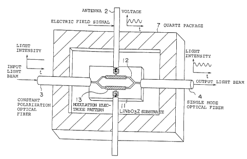
Fig. 4 is a slightly perspective view of an
optical electric field sensor according to a second
embodiment of this invention with an upper half of a
quartz package removed. A Mach-Zehnder interferometer
pattern was formed on a Z-cut substrate 11 (having a
crystal axis in a Z direction) of LiNb03 by a Ti pattern.
Then, optical waveguides 12 were formed by thermal
diffusion. Thereafter, an Si02 film was formed on a
surface on the optical waveguides 2. Modulation
electrode patterns 13 were formed thereon. For input and
output of a laser beam, the optical waveguide 12 was
subjected to face polishing. A constant polarization
_2144079
optical fiber 3 and a single mode fiber 4 were connected
to a light incident side and a light outgoing side,
respectively. Those elements thus manufactured had the
optical modulation characteristics as illustrated in Fig.
2 and described in the foregoing. Selection was made of
an optimum one as an optical electric field sensor.
Thereafter, antennas 6 for electric field detection were
connected to modulation electrodes 13. An entire
arrangement was housed in the quartz package 7. The
package was made up by the use of an organic adhesive and
sealed so that the internal element is not affected by an
outside air. For the sake of comparison, a conventional
optical electric field sensor was prepared by the use of
a package made of acrylic plastic. It was noted here
that those elements were selected to have a same optical
modulation characteristic.
In order to demonstrate the effect of this
invention, each element was wrapped by acrylic sponge and
left at the room temperature for one day with the
electrodes short-circuited, so as to generate an
electrostatic field by the package. Then, the optical
modulation characteristic of each optical electric field
sensor was measured. In the conventional optical
electric field sensor, fluctuation of the optical bias
was observed. On the other hand, no fluctuation was
found in the optical electric field sensor of this
invention. With respect to variation of the ambient
temperature, no fluctuation of the optical bias was
214~D79
16
observed in the optical electric field sensor of this
invention using the quartz package even in a condition
(10°C higher than the room temperature) where fluctuation
of the optical bias is caused in the conventional optical
electric field sensor with the package made of acrylic
plastic.
Similar comparison was made as regards another
optical electric field sensor according to this
invention. In this optical electric field sensor, the
quartz package was subjected to the abrasion process. In
this event, a more excellent result was obtained as
compared with the above-mentioned case. With the package
made of ceramics, a similar result was obtained as in _
case of quartz.
By the use of the package made of glass (quartz)
or ceramics, the above-mentioned optical electric field
sensor according to the second embodiment of this
invention achieves stable characteristics without
variation of the optical modulation characteristic after
assembling and without fluctuation of the optical bias in
response to the temperature variation from the room
temperature. Because heat insulation of the element is
stable in the optical electric field sensor according to
the first embodiment of this invention, no consideration
is required of the influence of the temperature drift as
far as it is used at the room temperature (mainly used in
an EMC measurement within a radio dark room, which is
carried out in an environment of the room temperature).
2144Q7~
17
It is therefore possible to provide an optical electric
field sensor manufactured with a high productivity by
removing a process for making any way against the
temperature drift.
By the use of such a technique in the second
embodiment of this invention, no electrostatic field is
generated by the package material and the influence of
the variation of the ambient temperature upon variation
of the temperature within the package is reduced.
(Third Embodiment)
Fig. 5 shows an electric field sensor according
to a third embodiment of this invention. As illustrated
in Fig. 5, an optical branched wave_guide type
interferometer is prepared on an LiNb03 substrate by
diffusion of Ti. One of two branched optical waveguides
is provided with electrodes. This optical modulator is
fixedly housed in a glass case 1. The electrodes of the
optical modulator are connected to antennas 2. A
polarization maintaining fiber 3 and a single mode fiber
4 are connected to a light incident side and a light
outgoing side of the optical modulator, respectively. A
combination of those components forms the optical
electric field sensor. In Fig. 5, the optical electric
field sensor is put in a condition where the ambient
temperature of the optical electric field sensor is 30°C.
A light beam is incident to the polarization maintaining
fiber 3 and passes through the optical electric field
sensor to be emitted from the single mode fiber 4 as a
214479
18
normal outgoing light beam having a waveform C. An
abscissa and an ordinate represent an applied electric
field and a light intensity, respectively. Herein,
adjustment is made so that the light intensity is located
at a middle point between the maximum level and the
minimum level when the electric field applied to the
antenna is equal to 0 (V). The foregoing structure is
similar to that of the first embodiment. The optical
electric field sensor according to the third embodiment
of this invention is different from the first embodiment
in that it is covered by expanded polystylene foam 5
having a heat insulation effect.
In the_optical electric field sensor according to
the third embodiment of this invention, a light beam is
incident to the polarization maintaining fiber 3 and
passes through the optical electric field sensor to be
emitted from the single mode fiber 4 as a normal outgoing
light beam having a waveform C as illustrated in Fig.
5(b). Adjustment of a zero point is carried out so that
the light intensity is located at a middle point between
the maximum level and the minimum level when the electric
field applied to the antenna is equal to 0 (V), as is
similar to the conventional case. However, as
illustrated in Fig. 5(c), a difference exists in that a
waveform D of the outgoing light beam emitted from the
single mode fiber 4 is coincident with the waveform C
without being subjected to the temperature drift.
Specifically, in the waveform D, the light intensity is
19
equal to 0 (V) when the electric field applied to the
antennas is equal to 0 (V). Thus, the waveform is not
varied from the waveform C of the normal outgoing light
beam. As described, the expanded polystylene foam 5
suppresses the temperature drift (see Fig. 1(c)) of the
optical electric field sensor to achieve an excellent
temperature characteristic and a stable sensitivity.
From the above-mentioned result, it is understood
that the optical electric field sensor using a material
having a heat insulation effect according to the third
embodiment of this invention can suppress the influence
of the temperature drift resulting from variation of the
_ ambient temperature to improve a temperature character-
istic and to keep a stable sensitivity of the sensor.
According to the third embodiment of this invention, the
influence of variation of the ambient temperature of the
optical electric field sensor upon the optical crystal of
the optical modulator is suppressed to be small. It is
therefore possible to provide an optical electric field
sensor having an excellent temperature characteristic.
According to the third embodiment of this invention, it
is possible not only to contribute to the improvement of
the temperature characteristic of the optical electric
field sensor, which is a problem in prior art, but also
to provide an optical electric field sensor manufactured
at a relatively low cost in a reduced process time with a
high productivity.
20
(Fourth Embodiment)
Fig. 6 shows a main portion of an optical
electric field sensor according to a fourth embodiment of
this invention. As illustrated in Fig_ 6, a Ti (film
thickness of 800A) thermal diffusion optical waveguide
(hereinafter simply called an optical waveguide) 12 was
formed on a X-cut substrate ll of LiNb03 crystal as a
branch interference type optical waveguide which is
branched and again joined together. Modulation
electrodes 13 were arranged in an area after branched and
before joined again. Thus, a Mach-Zehnder optical
interferometer 20 was manufactured_ On opposite ends of
the element, two short dipole antennas (not shown) of
75mm were connected to the modulation electrodes i3 in
the manner similar to Fig. 2. A constant polarization
optical fiber and a single mode optical fiber were
connected to a light input side and a light output side,
respectively (not shown). An input light beam was a
laser light beam having a wavelength of 1.3 ~am_ An
output light beam was subjected to 0/E (Optical Electrical)
conversion for measurement. A direct current voltage was
applied to the short dipoles of the optical electric field
sensor thus manufactured. A half-wavelength voltage V~ was
obtained from the intensity variation of the optical output in
response to the applied voltage.
By the use of a conductive spray of this invention, a
conductive resin film 14 was formed (process time being on
the order of 5 seconds per one) on the
CA 02144079 2001-02-14
2144U7~
21
optical modulator portion of the optical electric field
sensor thus manufactured. In a thermostatic chamber,
variation of the intensity of the outgoing light beam in
response to temperature variation was confirmed. The
temperature was varied stepwise by 10°C in a range
between -10°C and 60°C. For the sake of comparison, a
similar test was carried out for the optical electric
field sensor without treatment by the conductive spray.
The test data were dealt with in the form of voltage
shift which is obtained from the light intensity with
reference to an SG curve 25 in Fig. 7 and normalized by
the half-wavelength voltage V.
The optical electric field sensor without using
the conductive spray was unstable in light intensity, the
level of which fluctuated even around 25°C. With respect
to the temperature variation, a shift not smaller than
the half-wavelength voltage was confirmed. On the other
hand, the optical electric field sensor according to this
invention exhibited no variation in light intensity even
around 25°C. It was confirmed that the shift in the
optical bias is not greater than +0.3~ (normalized by the
half-wavelength voltage) in an environment of the
temperature between -10°C and 60°C.
The above-mentioned result shows that the fourth
embodiment of this invention is effective in improvement
of the temperature characteristic of the optical electric
field sensor. Also from the fourth embodiment, it is
confirmed that this invention greatly contributes to
~144a~a
22
improvement of productivity because manufacture is easily
carried out at a very low cost as compared with the
conventional case. Accordingly, it is found out that the
fourth embodiment of this invention provides an optical
electric field sensor with a conductive film formed by an
inexpensive and simple process.
(Fifth Embodiment)
Fig. 8 shows a main portion of an optical
electric field sensor according to a fifth embodiment of
this invention. As illustrated in Fig. 8, a Ti (film
thickness of 800A) thermal diffusion optical waveguide 12
was formed on a X-cut substrate 11 of LiNb03 crystal as a
branch interference type optical waveguide which is
branched and again joined together. Modulation
electrodes 13 were formed in an area after branched and
before joined again. Thus, a Mach-Zehnder optical
interferometer was manufactured in the manner similar to
the fourth embodiment. In the fifth embodiment, silicone
17 was applied onto a region including the modulation
electrodes 13 adjacent to the optical waveguide 12. On
opposite ends of the element, two short dipole antennas
of 75mm were connected to the modulation electrodes 13.
A constant polarization optical fiber and a single mode
optical fiber (not shown) were connected to a light input
side and an output side, respectively. An input light
beam was a laser light beam having a wavelength of 1.3
Vim. An output light beam was subjected to O/E conversion
for measurement. A direct current voltage was applied to
2144079
23
the short dipoles of the optical electric field sensor
thus manufactured. A half-wavelength voltage V.~ was
obtained from the intensity variation of the optical
output in response to the applied voltage. The result
was illustrated in Fig. 9. The optical electric field
sensor thus manufactured was applied with a DC voltage
(12V), which tends to cause characteristic deterioration,
and left for 100 hours. Then, the DC drift was measured.
Likewise, the sample without being applied with silicone
was measured for comparison.
After measurement, a test was carried out for 100
hours at a constant temperature and humidity of 60°C and
60~ which was a bad environment realized by the use of
common tap water for humidification. Then, the DC drift
was similarly measured. As a result, the time period
until the initial DC drift is caused was unchanged in the
sample applied with the silicone. On the other hand, the
time period was reduced more than 10 times in the sample
without being applied with the silicone. According to
the fifth embodiment of this invention, the agent having
a stable characteristic, namely, having no undesired ions
and a high reliability, is applied in an area between the
electrodes, where any foreign substance tends to invade.
It is therefore possible to provide an optical electric
field sensor which is capable of inhibiting interference
with an external environment to readily prevent invasion
of dirt or a foreign substance. It is confirmed that, by
the use of the optical electric field sensor according to
_~14407g
24
the fifth embodiment of this invention, a stable optical
electric field sensor is provided which can suppress
variation of the DC drift although a process is very
simple. In addition, according to the fifth embodiment
of this invention, it is possible to provide an optical
electric field sensor having a characteristic stable for
a long time, inasmuch as invasion of a foreign substance
is avoided during application of silicone. Since no
special facility is required and the operation itself is
very easy, no substantial increase in process time is
required.
(Sixth Embodiment)
Fig. 10 shows an optical electric field sensor
according to a sixth embodiment of this invention.
Referring to Fig. 10, a Mach-Zehnder interferometer
pattern similar to the conventional one illustrated in
Fig. 2 was formed on a Z-cut substrate 21 of LiNb03
crystal by a Ti pattern. Then, an optical waveguide 12
was formed by thermal diffusion. Thereafter, an Si02
film was formed on a surface of the optical waveguide 12.
A pattern of modulation electrodes 22 was formed thereon.
For input and output of a laser beam, the optical
waveguide was subjected to face polishing. A constant
polarization optical fiber 3 and a single mode fiber 4
were connected to a light incident side and a light
outgoing side, respectively. The element thus
manufactured has an optical modulation characteristic as
illustrated in Fig. 3, like in the conventional case.
_2144079
The foregoing structure is similar to that of the
conventional case. Thereafter, according to the sixth
embodiment of this invention, antennas 2 for electric
field detection were connected to the modulation
electrodes 22. An entire arrangement was packaged as
illustrated in Fig. 10. The antennas are'not illustrated
in Fig. 10. The package was made up by the use of an
organic adhesive and sealed so that the internal element
is not affected by an outside air.
By the use of two kinds of vinyl chloride plates,
namely, a vinyl chloride plate subjected to the
antistatic treatment according to the sixth embodiment of
this invention and a comparative vinyl chloride plate not
subjected to any treatment, the packages were
individually made up and subjected to measurement of
electric charge. At first, the above-mentioned two kinds
of packages were applied with electric fields of a same
intensity. After lapse of a predetermined time duration,
electric charges were measured and compared with each
other. As a result, after 30 seconds from application of
the electric field, no substantial electric charge was
observed in the antistatic-treated package according to
the sixth embodiment of this invention. On the other
hand, in the package of the comparative example without
any treatment, the electric charge was measured to
correspond to approximately a half of the intensity of
the applied electric field.
_2144079
26
The above-mentioned result shows that the optical
electric field sensor using the package according to the
sixth embodiment of this invention is capable of carrying
out optical modulation of an electric field to be
measured alone. This is because no disturbance or
influence is given to the ambient electric field by
electrification of the package. In addition, according
to the sixth embodiment of this invention, it is possible
to provide the optical electric field sensor which is
capable of removing an electrostatic field from the
package material after packaging so as not to disturb the
electric field to be measured. According to the sixth
embodiment of this invention, it is possible to provide
the optical electric field sensor which is capable of
measuring the electric field free from an influence of
disturbance by removing the electrostatic field generated
from the package material even if the plastic material is
used. According to the sixth embodiment of this
invention, it is possible to provide the optical electric
field sensor which has an excellent temperature
characteristic, by suppressing the influence of the
variation of the ambient temperature around the optical
electric field sensor upon the optical crystal of the
optical modulator. According to the sixth embodiment of
this invention, it is possible not only to contribute to
improvement of the temperature characteristic of the
optical electric field sensor, which has been a problem
in prior art, but also to provide the optical electric
2144079
27
field sensor manufactured at a relatively low cost in a
reduced process time with a high productivity.
As described above, according to the first
through the sixth embodiments of this invention, it is
possible to provide the optical electric field sensor
having a structure of suppressing heat conduction of
thermal fluctuation outside of the optical electric field
sensor to the optical crystal so that any device of a
high accuracy is unnecessary and the temperature
characteristic is improved.
(Industrial Application Field)
As described above, the electric field sensor
according to this invention is adapted to measurement of
an electric field intensity within a spatial field,
typically, EMC measurement (noise measurement).