Note: Descriptions are shown in the official language in which they were submitted.
w 2144087
(Translation)
SPECIFICATION
OPTICAL MODULATION SYSTEM
Technical Field
This invention relates to an optical modulation
system for modulating a light beam transmitted through an
optical waveguide by applying an external electric field.
Background Art
There is known a conventional optical modulation
- system comprising a light source, an optical device
supplied with a light beam from the light source, and an
electric field applying device for applying an electric
field to the optical device. The optical device
comprises a substrate, an incident optical waveguide
formed on the substrate for receiving the light beam
incident thereto, two phase-shift optical waveguides
formed on the substrate to be branched from the incident
optical waveguide for varying a phase of a transmitted
light beam in response to an electric field intensity,
and an outgoing optical waveguide formed on the substrate
to join the phase-shift optical waveguides.
In the conventional optical modulation system,
however, a phase difference is caused between the
branched optical waveguides even if the intensity of the
applied electric field is equal to zero, depending upon
2144087
2
manufacturing conditions of the optical waveguides. This
results in fluctuation of a ratio of the variation of
light intensity relative to the variation of the applied
electric field, namely, fluctuation of an optical
modulation efficiency.
In addition, the conventional optical modulation
system is disadvantageous in that the optical device
tends to deteriorate when the magnitude of the applied
electric field is great.
It is an object of this invention to provide an
optical modulation system capable of readily adjusting a
phase difference when the intensity of an applied
electric field is equal to zero.
It is an object of this invention to provide an
optical modulation device capable of avoiding
deterioration of an optical device even if the magnitude
of an applied electric field is great.
Disclosure of the Invention
This invention is characterized by provision of a
substrate, an incident optical waveguide formed on the
substrate for receiving a light beam incident thereto,
two phase-shift optical waveguides formed on the
substrate to be branched from the incident optical
waveguide for varying an intensity of a transmitted light
beam in response to a phase of an electric field, and an
outgoing optical waveguide formed on the substrate to
join the phase-shift optical waveguides, at least one of
the phase-shift optical waveguides having a reversely
2144087
3
polarized portion reversely polarized.
This invention is also characterized by provision
of a substrate, an optical waveguide formed on the
substrate for varying an intensity of a transmitted light
beam in response to an intensity of an electric field,
and a light transmission film formed at one or a
plurality of areas on the optical waveguide.
This invention is also characterized by a buffer
layer formed at a part on or in the vicinity of the
phase-shift optical waveguides.
This invention is also characterized by a buffer
layer formed at a part on or in the vicinity of the
phase-shift optical waveguides, and a transparent
substance film formed on a part or a whole of a portion
without the buffer layer for imparting a stress on the
phase-shift optical waveguides.
This invention is also characterized by a stress
imparting member for imparting a stress to a part of one
of the phase-shift optical waveguides.
This invention is also characterized by a light
irradiation unit for irradiating a light beam onto a part
or a whole of one of the phase-shift optical waveguides.
Brief Description of the Drawing
Fig. 1 is a front view of an optical modulation
system according to this invention.
Fig. 2 is a front view of another embodiment of
this invention.
2144087
4
Fig. 3 is a view for describing a characteristic
of the embodiment in Fig. 2.
Fig. 4 is a view for describing another
characteristic of the embodiment in Fig. 2.
Fig. 5 is a perspective view of another
embodiment of this invention.
Fig. 6 is a perspective view of another
embodiment of this invention.
Fig. 7 is a view for describing a characteristic
of the embodiment in Fig. 6.
Fig. 8 is a perspective view of another
embodiment of this invention.
Fig. 9 is a perspective view of another
embodiment of this invention.
Fig. 10 is a perspective view of another
embodiment of this invention.
Fig. 11 is a view for describing a characteristic
of the embodiment in Fig. 10.
Fig. 12 is a perspective view of another
embodiment of this invention.
Fig. 13 is a perspective view of another
embodiment of this invention.
Fig. 14 is a perspective view of another
embodiment of this invention.
Fig. 15 is a perspective view of another
embodiment of this invention.
Fig. 16 is a front view of another embodiment of
this invention.
2144087
Fig. 17 is a perspective view of a main portion
of the embodiment in Fig. 16.
Fig. 18 is a front view of another embodiment of
this invention.
Embodiment
Now, description will be made in detail as
regards several embodiments of this invention with
reference to the drawing.
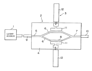
Fig. 1 is a front view of a first embodiment of
this invention. As illustrated in Fig. 1, an optical'
modulation system according to this invention comprises a
light source 1, an optical device 2 for receiving a light
beam from the light source 1, and an electric fief d
applying device 3 for applying an electric field to the
optical device 2. The optical device 2 comprises a
substrate 4, an incident optical waveguide 5 formed on
the substrate 4 for receiving the light beam incident
thereto, two phase-shift optical waveguides 6 formed on
the substrate 4 to be branched from the incident optical
waveguide 5 for varying a phase of a transmitted light
beam in response to an intensity of an electric field,
and an outgoing optical waveguide 7 formed on the
substrate 4 to join the phase-shift optical waveguides 6.
At least one of the phase-shift optical waveguides 6 has
a reversely polarized portion reversely polarized.
The light source 1 and the incident optical
waveguide 5 are connected through an incident optical
fiber 9. The light beam from the light source 1 is
2144087
6
incident through the incident optical fiber 9 to the
incident optical waveguide 5 and branched by the two
phase-shift optical waveguides 6 into branched beams
which are again combined together in the outgoing optical
waveguide 7. The outgoing optical waveguide 7 is
connected to an outgoing optical fiber 10. The light
beam after combined together in the outgoing optical
waveguide 7 is emitted through the outgoing optical fiber
10.
The electric field applying device 3 comprises
two modulation electrodes 11 formed on the substrate 4
and located on or in the vicinity of the phase-shift
optical waveguides 6, and antennas 12 connected through
lead wires to the modulation electrodes 11, respectively.
When a reception signal is received by the antennas 12,
the modulation electrodes 11 apply predetermined electric
fields to the phase-shift optical waveguides 6.
Depending upon the intensities of the electric fields,
the refractive indexes of the phase-shift optical
waveguides 6 are varied. This results in variation of
phases of the light beams transmitted through the
phase-shift optical waveguides 6. The reversely
polarized portion 8 has an optical axis direction
different from that of the remaining portion of the
phase-shift optical waveguides 6 except the reversely
polarized portion 8 and, accordingly, provides the
transmitted light beam with a reverse phase shift reverse
to that given by the remaining portion when a uniform
.,.
zm4os7
electric field is applied to the substrate 4. This
results in variation of an intensity of an outgoing light
beam.
Next, description proceeds to a specific example
of the first embodiment of this invention.
The substrate 4 was formed from a Z-cut lithium
niobate (LiNb03) crystal plate. On the surface of the
substrate 4, the incident optical waveguide 5, the
phase-shift optical waveguides 6, and the outgoing
optical waveguide 7, having a width of 8 j.zm and a depth
of 6 Vim, were formed by thermal diffusion of Ti. A part
of the phase-shift optical waveguides 6 that is to serve
as there-versely polarized portion 8 has a length of
25mm. A distance between parallel portions of the two
phase-shift optical waveguides is equal to 20 Vim.
An Si02 layer was deposited to a thickness of
about 0.5 ~m on the substrate 4, the incident optical
waveguide 5, the phase-shift optical waveguides 6, and
the outgoing optical waveguide 7. Through photoresist
patterning and Si02 etching, a part of one of the two
phase-shift optical waveguides 6 was exposed.
Then, a heat treatment was carried out at 1000°C
for two hours in a wet oxygen atmosphere. After
completion of heating, natural cooling was carried out in
an electric furnace. Thus, the reversely polarized
portion 8 of the phase-shift optical waveguides 6 was
formed. The Si02 left on the crystal surface was removed
by the use of a buffer etching fluid.
2144087
8
The optical device thus manufactured was
connected to the incident optical fiber 9 which is a
polarization plane maintaining fiber and to the outgoing
optical fiber 10 which is a single mode fiber. The light
source 1 comprises a laser which has a propagation laser
beam wavelength of 1.31 ~.zm.
As illustrated in Fig. 2, the optical device 2
which is a Mach-Zehnder interferometer was manufactured
as an embodiment of this invention by the use of the
LiNb03 substrate 4 cut along an X axis. Manufacturing
conditions are as follows. Thermal diffusion (at 1025°C
for five hours in a wet 02 atmosphere) was carried out by
_ the use of Ti having a thickness of 800 angstroms. The
modulation electrodes 11 for applying an applied voltage
to the branched phase-shift optical waveguides 6 in a
C-axis direction of the substrate 4 were formed by vapor
deposition of Cr-Au.
By sputtering Si02 to a thickness of 1500~um, a
light transmission film 13 was formed at a part (having a
width of 15 mm) of one of the branched optical waveguides
6 of the optical device 2. In case where the
conventional optical device having no light transmission
film 13 is applied with the voltage, the intensity of an
optical output varies along a curve A illustrated in Fig.
3. On the other hand, when the optical device 2 having
the light transmission film 13 is applied with the
voltage, the light intensity varies along a line B
illustrated in Fig. 3. From this, it has been proved
214408
9
that the phase of the optical device 2 can be adjusted
according to this embodiment.
Fig. 4 shows one example of the data about output
variation with respect to the thickness of the light
transmission film 13. As is clearly seen, when the light
transmission film 13 comprising an Si02 film is formed by
a sputtering process, the shift amounts in output bias
are equal to~rc/8 and ~/4 for the film thickness of 500
angstroms and 1000 angstroms, respectively. The element
used has a half-wavelength voltage of 1.5 V. In this
description, the bias indicates a point on the curve of
the optical output intensity in Fig. 3 when no voltage is
applied to the optical waveguide.
As illustrated in Fig. 5, the optical device 2
comprises the incident optical waveguide 5, the
phase-shift optical waveguides 6, and the outgoing
optical waveguide 7 which are formed on the LiNb03
substrate 11 by thermal diffusion of titanium at a
temperature between 900 and 1100°C for several hours and
which have a width between 5 and 12 ~m and a depth
between 3 and l0~um.
A buffer layer 14 of Si02 is formed on the
incident optical waveguide 5, the phase-shift optical
waveguides 6, the outgoing optical waveguide 7, and the
substrate 4. On the buffer layer 14, the modulation
electrodes 11 having a width between 10 and 30 ~m are
formed. A part of the buffer layer 14 that is positioned
on one of the phase-shift optical waveguides 6 is cut
2144087
1~
away to form an opening 15.
As illustrated in Fig. 6, in the optical device
2, a portion without the Si02 buffer layer 14 is
partially coated with a substance, such as a
cyanoacrylate adhesive 16, for imparting a stress onto a
part of the phase-shift optical waveguide 6. The
adhesive 16 serves to vary the refractive index of the
phase-shift optical waveguide 6 so as to provide a phase
difference between two phase-shift optical waveguides 6.
The light intensity characteristic when the voltage is
applied to the optical device 2 in Fig. 6 is changed from
that depicted by a curve C to that depicted by a curve D
in Fig. 7.
As illustrated in Fig. 8, in the optical device
2, a plurality of openings 15 may be formed through the
buffer layer 14 on the phase-shift optical waveguide 6.
As illustrated in Fig. 9, in the optical device
2, a plurality of openings 15 may be formed through the
buffer layer 14 on the phase-shift optical waveguide 6
with the adhesive 16 filled in a predetermined number of
openings 15 among those openings 15 to coat the
phase-shift optical waveguide 6.
According to this embodiment, it is possible to
provide a desired optical phase difference after
manufacture of the incident optical waveguide 5, the
phase-shift optical waveguides 6, and the outgoing
optical waveguide 7.
2~~4ag~7
--- -
11
Third Embodiment
Description will now be made as regards a third
embodiment of this invention with reference to the
drawings.
As illustrated in Fig. 10, the optical device 2
comprises the substrate 4 with the incident optical
waveguide 5, two phase-shift optical waveguides 6, the
outgoing optical waveguide 7, and the modulation
electrodes 11 formed on the substrate 4.
The incident optical waveguide 5, the phase-shift
optical waveguides 6, and the outgoing optical waveguide
7 are formed by thermal diffusion of titanium (Ti) on the
substrate 4 at a temperature between 900 and 1100°C for _
several hours. The incident optical waveguide 5, the
phase-shift optical waveguides 6, and the outgoing
optical waveguide 7 have a width between about 5 and l2~um
and a thickness between about 3 and 10 dam. The modula-
tion electrodes 11 have a width between 10 and 30 ~m.
The buffer layer 14 is formed on the substrate 4,
the incident optical waveguide 5, the phase-shift optical
waveguides 6, and the outgoing optical waveguide 7. The
buffer layer 14 is made of Si02. On the upper surface of
the buffer layer 14, the modulation electrodes 11 are
formed. The modulation electrodes 11 have a width
substantially equal to 10 ~.zm.
The substrate 4 has two side surfaces parallel to
the light transmission direction. Stress imparting
members 17 are arranged on the side surfaces in contact
214408
12
therewith. The stress imparting members 17 are made of a
piezoelectric semiconductor. Being applied with a
predetermined voltage, the stress imparting members 17
are deformed to impart a stress to the phase-shift
optical waveguides 6 through the substrate 4. When the
stress is imparted, the refractive indexes of the
phase-shift optical waveguides 4 are varied so that the
phases of the light beams transmitted through the
phase-shift optical waveguides 6 are shifted.
For example, without any stress imparted by the
stress imparting members 17 to the phase-shift optical
waveguides 6, the intensity of the outgoing light beam is
varied in response to variation of the applied voltage,
as depicted by a curve E in Fig. 11. In this event, by
the use of the stress imparting members 17 for imparting
the stress to the phase-shift optical waveguides 6,
adjustment can be made so that the intensity of the
outgoing light beam is varied in response to the
variation of the applied voltage, as depicted by a curve
F in Fig. 11.
As illustrated in Fig. 12, the optical device 2
is accommodated in a package 18. The package 18 is
provided with a threaded hole 19 formed on a part
thereof. A screw 20 is engaged in the threaded hole 19.
The screw 20 constitutes the stress imparting member 17.
A top end of the screw 20 is adapted to be pressed
against the phase-shift optical waveguide 6. When the
screw 20 imparts the stress to the phase-shift optical
2144087
13
waveguide 6, the refractive index of the phase-shift
optical waveguide 6 is varied.
As illustrated in Fig. 13, the screw 20 may press
the substrate 4 in the vicinity of the phase-shift
optical waveguide 6 so as to impart the stress to the
phase-shift optical waveguide 6.
As illustrated in Fig. 14, in case where the
optical device 2 has the buffer layer 14, the screw 20
may press a part of the buffer layer 14 that is located
on the phase-shift optical waveguide 6 so
as to impart the stress to the phase-shift optical
waveguide 6.
As illustrated in Fig. 15, in case where the
optical device 2 has the buffer layer 14, the screw 20
may press a part of the buffer layer 14 that is located
in the vicinity of the phase-shift optical waveguide 6 so
as to impart the stress to the phase-shift optical
waveguide 6.
As illustrated in Figs. 16 and 17, the optical
device 2 is accommodated in a package 21 having a thermal
plasticity. The optical device 2 is fixed through
silicone to a fixing table 23 formed on a bottom 22 of
the package 21. To end faces of the incident optical
waveguide 5 and the outgoing optical waveguide 7 of the
optical device 2, the incident optical fiber 9 and the
outgoing optical fiber 10 are connected, respectively.
The antennas 12 are connected through lead wires 24 to
the modulation electrodes 11 of the optical device 2. An
_2144087
14
ultraviolet ray is irradiated by an ultraviolet
irradiation unit onto a predetermined part 25 of the
bottom 22 of the package 21. The bottom 22 of the
package 21 is thereby heated and deformed to impart the
stress to the phase-shift optical waveguides 6. In case
where the substrate 4 is accommodated in the package 21
in contact with the internal wall thereof, the substrate
4 need not be fixed to the package 21 by the use of the
adhesive.
Fourth Embodiment
Next, a fourth embodiment of this invention will
be described in detail with reference to the drawings.
As illustrated in Fig. 18, the optical device 2
comprises the substrate 4, the incident optical waveguide
formed on the substrate 4 for receiving the light beam
incident thereto, two phase-shift optical waveguides 6
formed on the substrate 4 to be branched from the
incident optical waveguide 5 for varying the intensity of
the transmitted light beam in response to the intensity
of the electric field, the outgoing optical waveguide 7
formed on the substrate 4 to join the phase-shift optical
waveguides 6, and a light irradiation unit 26 for
irradiating a part or a whole of one of the phase-shift
optical waveguides 6.
The substrate 4 is made of lithium niobate
(LiNb03) or the like. When the light beam is irradiated
onto an electrooptical crystal such as lithium niobate,
electrons in the crystal are excited from an impurity
_ _2I44Q87
level to a conduction band so that the electrons are
drifted in a +Z direction. During the drift, the excited
electrons fall into a trap level. Accordingly, positive
and negative portions are produced in the crystal to
generate a space electric field. The space electric
field brings about variation of the refractive index.
This phenomenon is called an optical damage. This
invention makes use of this phenomenon.
For example, the incident optical waveguide 5,
the phase-shift optical waveguides 6, and the outgoing
optical waveguide 7 are formed on the substrate 4 of
lithium niobate by thermal diffusion of Ti. The thermal
diffusion is carried out at a temperature of 1025°C for
five hours in a wet 02 atmosphere. The incident optical
waveguide 5, the phase-shift optical waveguides 6, and
the outgoing optical waveguide 7 have a thickness of 500
angstroms and a width of 6 ~m.
The optical device 2 has an insertion loss of 5.5
dB, an extinction ratio of 26.0 dB, and a half-wavelength
voltage of 1.9 V.
Industrial Applicability
This invention is adapted for use in an optical
switch and an optical modulation system requiring a phase
control. This invention can be used also as an electric
field sensor for measuring an intensity of an electric
field.