Note: Descriptions are shown in the official language in which they were submitted.
WO94/07350 ~ Q~ PCI`/US93/08426
.
-1-
HERMETICALLY SEALED CIRCUIT MODULES HAVING
CONDUCIIVE CAP ANCHORS
R~AcKGRouND OF T~F INVE~TION
This invention relates to hermetically sealed clcc~ol~.c
5 circuit mo~ s.
Circuit moflllles have been hermetically sealed to protect
the se~ ive circuit components from harsh ell~.lo.. -ont~l con~ nc.
Heretofore, it has been .liffi~llt to provide conductive paths between
circuit components within the package to te~ ;on pads ~Ytçm~l of the
10 package. Typically, chips or other circuit co~ ollents are mollnte~l in the
package to one side of a wiring board or substrate and are electrically
connecte~ to te~ ;on pads within the h~rmetic~lly sealed region.
~onAuctive vias extend vertically through the board or substrate to
connect the internal pads to pads outside the hermçtir~lly sealed region.
15 The con-lllctive vias are co~llucted by well-known plated-through or
plated-up hole technillues by which holes in the board or substrate are
plated or filled with con~lllctiye material to form the con~lllctive vias.
Altelllalively, the vias may be formed by a deposition process. An
example of the use of con-lnctive vias to ~ccomrlish ~Y~e~ 1 cQnnection
20 in hermetically sealed moclnlec may be found in U.S. Patent No.
4,560,826 granted December 24, 1985 to Burns et al.
The fabrication of the condllctive vias require procçccin.
steps during the collsll . ction of the wiring board and/or substrate which
are not normally incurred in proceccing the board. More particularly,
25 con-l~lctive vias were employed in prior herrnetic~lly sealed modules only
to extend through the board or substrate for çYtern~l connPction
Concequently, fo",.~1;on of these vias represented ~rlrlition~l procescing
steps which added significantly to the cost of the module.
Another difficulty with hermetically sealed elec~ollic
30 packages and mocl~ o,c resides in the adequacy of the seal itself. Prior
packages employed a metal ring and lid bonded by glass solder to a
WO 94/07350 ~4~S8 Pcr/US93/08~t26
t
-2-
ceramic substrate. The glass in~ ted the ring from the wiring board to
permit leads to pass thereunder from the region inside the sealed mo~ e
to the eYtern~l portions. One tlif~i~llty with such a metal-glass-ceramic
co,lsl,uction is that c~ o.~ nt~l con~litionC, such as ~iCSSul~ and r
temper~lulc v~ri~tion~, cause fatigue in the glass solder and failure of the
seal. An example of the use of glass bonding of hermetic seals to
packages may be found in U.S. Patent No. 4,925,024 granted May 15,
1990 to Ellenberger et al.
To ovelcon~e the problems ~ccoci~te~l with metal seals,
sealing rings constructed of a m~teri~l more closely " -~ ~cl~ the th.orm~l
ciorl char~ctçri~ti~ of the ceramic substrate have been employed.
For eY~mrlet an iron-nickel-cobalt alloy ~ eted under the tr~dem~rk
KOVAR provides good therm~l m~tching char~ ter~tit~c to the ceramic
substrate. Also, KOVAR is provides good magnetic .~hieltlin~, Hu~cr,
the iron-nickel-cobalt alloy is .liffi~llt to attach to ceramic sub~llates.
C'once~uently, met~li7e~l ceramic sealing rings were used having KOVAR
rings or flanges brazed thereto. An example of the use of KOVAR
flanges brazed to ceramic sealing rings is found in U.S. Patent No.
4,076,955 granted February 28, 1978 to Gates, Jr.
R~FF nF~c~ IoN OF THF INVFNTION
In one form of the invention, a circuit mr~ le in~lllcles a
mllltil~yer circuit board having a plurality of ~ltern~te layers ~l.o.fining
circuit paths which are separated by incnl~tion layers. Con~ ctive vias
extend between selected circuit paths of di~ele.ll layers. A hermetic seal
is sealed to the top layer of the mnltil~yer circuit board to en~lose circuit
co~ onents in a hermetically sealed region. Selected circuit paths
and/or vias are connected to external pads outside the sealed region by
vias eYten-ling through selected layers of the multilayer circuit board, one
via termin~ting internally to the sealed region and another via
30 te~ t;g at the external pad.
WO 94/07350 2 1 ~ ~ 0 8 8 Pcr/uss3/o8426
-3-
In a first option, the vias providing the external cQnn~ction
extend into a substrate supporting the board, and circuit paths in the
substrate electrically connect the vias together.
In a second option, the vias providing the ~Ytern~l
S connection are electrically connected together by selected circuit paths
in the circuit board.
Acco~ul~g, to another form of the i~ ulioll, a coT~d~lctive
anchor eYt~n~1~ through the circuit board to the substrate and provides an
anchor for the seal. Advantageously, the conductive anchor forms a
con~ ctive wall sullu~ ng the circuit paths within the hermetically-
sealed region to ~nh~nre ~hielding from stray ele~iç~l and m~gn.otic
fields. In the option where the vias providing ~Yte~n~l connection are
cQnnected by selecte~l circuit paths in the circuit board, the con-lllctive
anchor coul~lises posts having openin~ through which the selecte~
circuit paths pass.
RRIEF DF~CRIPTION OF T~F DRAW~I~GS
Figure 1 is a perspective view of a hermetically sealed
electronic circuit module in accordallce with the ~les-nlly plefellcd
embo~lime-nt of the ~resclll invention, the m(l~lle being shown col~ected
to a mother board.
Figure 2 is a pe.~ecti~,e view, as in Figure 1, of the
hermetically sealed mo~lllle
Figure 3 is a section view taken at line 3-3 in Figure 2
showing a preferred embodiment of the present invention.
Figure 4 is a section view, as in Figure 3, showing a
mnflific~tion of the present invention.
Figure 5 is a section view of the a~ al ls illustrated in
Figure 4 taken along a plane parallel to section plane of Figure 4.
Figure 6 is a perspective view, as in Figure 1, illuslla~ g~
the method of ~tt~hing cond~lctive leads to the electric module of Figure
2.
WO94/07350 ~ PCI/US93/084~6
Figure 7 is an enlarged perspective view, as in Figure 6, of
a portion of the apparatus illustrated in Figure 6.
nF~TA~F~n DESCRIPI'ION OF TE~F P~FFF.~F.n
F~ RonIMFNTs
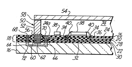
Figure 1 is a perspective view of a circuit modllle 10 in
accorda~ce with the present invention conn~cted to mother board 12 by
leads 14. As shown in Figures 2 and 3, circuit module 10 inr~ e~
substrate 16 on which is mounted ml~ltil~yer wiring board 18. Substrate
16 is ~refelably collsllucted of ceramic, such as AlN, A1203, BeO, or SiC.
lUnltil~yer board 18 is a sandwich COlll~lisillg a plurality of first layers 20,22 having selected con~hlctive circuit paths 24 d~o-fin~ therein, paths 24
being constructed of a suitable cQn-l~lctive material such as copper. A
plurality of second layers 26, 28 and 30, constructed of snit~hle in~ tQr
material such as polyi_ide or ~h-"~ "" oxide (A1203), s~ar~les layers
20 and 22 and the con~uctive paths 24 therein. Layers 20 and 22 also
in~ lde polyimide or ~l,.. ~,;,.. oxide in~nl~tor m~teri~l 32 in the areas
of layers 20 and 22 where circuit paths 24 are not present, m~tçri~l 32
acting as a spacer between adjacent in~ tor layers. ron~lllctive vias 34
are col~llucted of copper and extend between top sllrf~çe 36 of board 18
and sçlecte~l ones of the circuit paths 24 in sçlçcted layers 20, 22.
~'-on~lçtive vias 34 may be constructed by deposition techniques during
the forrn~tion of the s~lcce~!~ive layer of board 18, or may be co~llucted
by techniques employing plated-through or plated-up holes, well known
in the art. Electrical colll~onents 38, such as sçmiçQndllctQr chips, are
mollnte~l to top surface 36 of board 18 and are electrically connçcted by
leads 40 to con~ ctive pads formed by vias 34.
A hermetic seal 50 colll~lises a skirt 5~ and lid 54, both
~l~fe~ably consllucted of a iron-nickel-cobalt alloy such as KOVAR.
Seal 50 is fastened by ~-lherin~ skirt 52 to surface 36 of mllltil~yer board
18 with a conductive adhesive or a con~llctive solder 56. Lid 54 is
~tt~he~l to skirt 52 by con-11lctive adhesive 58.
WO 94/07350 21 44Q8 8 PCI`/U593/08426
Con~ ctive anchor 60 is forrned by successive copper layers
in each layer of printed m~lltil~yer board 18. In the embo~iim~ont shown
in Figure 3, anchor 60 incltldes at least a portion 62 form~d in substrate
16 at the interface with mllltil~yer board 18. C~ond~lctive vias 64 and 66
S co~~ cted of copper extend between cond~lctive path 72 in substrate 16
and a selected cond~l~ive pad 68 or 70 on surface 36 of board 18. Vias
64 and 66 may be formed by deposition of copper during the fo~ ;Qn
of each layer of board 18, or may be formed employing plated-through
or plated-up hole tec~niqllçs. Advantageously, vias 64 and 66 are formed
10 during the ~ ctnring ~ioces~ of board 18, using the same process
steps as is employed to form vias 34. Via 64 tel...;.~es at pad 68 on
snrf~ce 36 of the board, whereas via 66 te....;..~tes at either pad 70 on
s~ ce 36 or at a selected circuit path 24a within the board, or both as
shown in Figure 3. Pad 70 or circuit path 24a is connecte~ to one or
15 more circuit components 38 inside the h~rmetiç~lly sealed region 74 of
the module.
Skirt 52 and lid S4 together provide a cap 50 to
hermetically seal region 74 from the ellvilo~ ent ontcide the cap. Thus,
components 38 mo~lnted to the circuit board within region 74 are
20 hermetically seal from the ellvi-olllncnt.
Flectriç~1 connection of components 38 to pads outside
region 74 is ~comrlished through vias and circuit paths formed during
the rol...A~;on of board 18. Thus, vias 34, 64 and 66 are colls~ cted with
well known deposition techniques, plated-through hole techniques, or
25 plated-up hole techniques during the fab~tio~ of board 18. LLkewise,
the s~lçce~;ve layers fo....;.~g anchor 60 are formed by well known
deposition techniques during the fo~ ;on of the sllcce~ c layers of
mnltil~yer board 18. That portion 62 of anchor 60 and those portions of
vias 64 and 66 and con(lnctive path 72 formed in the substrate are
30 pl~formed in the substrate before ~tt~-~hing circuit board 18 to the
substrate.
W094/073~0 ~ 4~ 6- Pcr/US93/08426
In one form of the invention, con~ ctive anchor 60 forrns
a wall ~urloullding hermetically sealed region 74. Anchor 60, eYten-lin~
through board 18 to substrate 16, cooperates with seal 50 to provide a
shield against stray electric and magnetic fields for the colll~ollents 38
5 within region 74. Thus, stray magnetic and ele~1l0slaLic inter~erence
ollt~i~le the hermetic package is shielded out of the region 74. Moreover,
the anchor 60 forms a sturdy base for seal 50 which is re3;~ l to stress
caused by v~ri~tion in temperature and ~lc;,~urc on the p~ ge which
might otherwise cause fatigue on solder joint or con-lllctive adhesive 56.
10 Thus, with anchor structurally embedded in board 18, structural inte~rity
is provided for the seal and anchor, without resollillg to ~d~lition~l
SU~)~)Ol ~ flanges and the like required by the prior art.
Figures 4 and 5 illusllate a mnflific~tion of the pres~
invention in which selected circuit paths 80 within a selecte~l layer 22 of
the mllltil~yer board 18 connect vias 64 to vias 34. Figures 4 and 5 are
section views taken in parallel planes with Figure 4 being a sectirn view
through the pads and connection means between region 74 and the
external portion of the modllle~ and Figure S being a section view
between ~rlj~e.nt pads and connection means. In the emborlim~nt shown
in Figures 4 and 5, vias 34 te.. ~ e at a pad to which a co~ ullenl 38
is ~tt~che~l ~ltern~tively~ a via 34 may be connected to a diL~ercnl
circuit path 24. As shown particularly in Figure 5, cap 50 is anchored to
substrate 16 by cQn~ ctive anchor posts 82 formed in the layers in the
circuit board 18. The a~ gelllent shown in Figures 4 and 5 provides the
25 advantage of employing a con(lllctive path in a layer of board 18 between
posts 82 to provide external connection without the need to extend into
the substrate, as in Figure 3. The arrangement of Figures 4 and 5
provides somewhat reduced field shielding and somewhat reduced
structural support for the seal than the arrangement of Figure 3, although
30 ~hieltling and anchor sup~oll are adequate for most purposes.
WO 94/07350 21 4 4 ~ 8 ~ PCI/US93/08426
O
-7-
Figures 6 and 7 illustrate a techni(lue for ~tt~rhing
con~ çtive leads 14 to the hermetic package and particularly to pads 68
't thereof. Leads 14 initially are connected to or integral with a common
support strip 90. Leads 14 have a prescribed width W and thiclrnocc T
v S and are pocition~d at a prescribed pitch P (as m~ ,d between the
centers of sl cces~ leads). As eY~mrlec, leads 14 may have a width W
l~et-.~ en 0.002 and 0.012 inches, a thirlrnesC T between 0.0014 and 0.006
inches, and a pitch P between 0.004 and 0.025, ~epçn~ling upon their
intçn~ed appliç~tion The leads are intergal with commnn support strips
10 90 which include a row of sized ~lJellulcs 92 to aid in severing the
support strip to a desired length to match a side of the mt ~lnlç
Conveniently, leads 14 are f~hric~ted with at least twice the desired
length, with support strips 90 at both ends for structural SU~)O1 L during
r~ctnre and transportation. The lead structure may be supplied in
15 rolls so that a selected portion may be removed for use in ,, ~ r~ lr
a modllle~
In use, the leads are severed at the midpoint between the
:iU~Oll strips, resnltir~ in lead structures as shown in Figures 6 and 7
sul,~olled by a single support strip 90. The support strip is severed
20 through selected apertures 92 to a desired length to match the eYtçrn~l
pad confi~lration of the module. Module 10 is positionPd in a sized
opening 97 in tool 94, and the lead ~cc~mhly collllJr;sillg leads 14 and
su~oll strip 90 are pocitione~ on flat surface 95. Tool 94 in~ cles a
plurality of first locator pins 96 arranged to be rcceived in selected
a~el lul es 92 of SU~O11 strip 90. As shown particularly in Figure 7, with
module 10 pocitione~l in opening 97 and common ~u~oll strip 90
pocitioned on tool 92 with pins 96, leads 14 directly align with individual
pads 68 on moclllle 10.
Tool 94 in~ les a second plurality of locator pins 98
arranged to be received in apertures in non-con-lllctive tie bar 100. Tie
bar 100 serves to clamp leads 14 in position against surface 95 while the
W094/07350 ~Q~ Pcr/US93/08426
leads are tinned and soldered to pads 68. Conveniently, fastener means,
not shown, may be employed to hold the damped ~ccemhly together
during tinning and/or soldering.
While common support strip 90 may be severed and
5 removed from leads 14 before or after tinning and soldering the leads to
pads 68, it is ~lcfellcd that the common support strip be removed before
tinning and sol~ rin~ More particularly, with common Su~oll strip 90
removed and cl~mring provided by the non-conductive tie bar, there are
no reactive forces l~ led by the su~oll strip between the several
leads 14 which mighe interfere with the poCitioning of leads 14 to pads 68.
Hence, the individual leads co"ro, ..l to the height or position of the pads
without interference from the comm( n ~u~oll strip or the other leads.
The present invention provides an effective and econr)mic
teçhnillue for .~ r~lring hermetically sealed elccllullic modules
15 having con~ çtive paths from the interior of the mo~ e to condllçtive
pads at the eYt~rior. The invention also provides a s~lpe-rior seal and
connPction of the seal, for both hermetically sealing the ellviron~ ont of
the p~ ge from the eYtern~1 ellvil5~.. ~nt and to provide good chi.o~
from electric and m~gnlotic field interferences. While the advantages of
20 the pleselll invention have been described in connection with cQnd~lctive
paths using a mnltil~yer board and the use of a condllçtive anchor, each
of these features is might be employed to great advantage without
employing the other feature. For example, a condllçtive anchor for a seal
ight be employed with cQn~ ctive paths eytentlin~ through the seal,
25 rather than under it as shown in the dl~wi~, or the con-lll~ive paths
might employ techniques other than m~lltil~yer circuit techniques.
Likewise, con~lllçtive paths for e~le,..~l connection might be
~ccomplished using mllltil~yer circuit techniq~les without employing the
cond~lçtive anchor.
Although the present invention has been described with
rcÇelence to ~refelled embo~lim~nt~, workers skilled in the art will
WO 94/07350 2 1 4 4 û 8 8 Pcr/uss3/08426
g
recognize that changes may be made in form and detail without d~al ling
from the spirit and scope of the invention.