Note: Descriptions are shown in the official language in which they were submitted.
2144247
1 93-CON-157 (A UJ
DIRECT CIRCUIT BOARD CONNECTION
BACKGROUND OF THE INVENTION
The present invention relates to electrical interconnection between
separate circuit boards and particularly relates to making electrical
interconnection between circuit boards of a type having the circuitry etched
on
a metal foil laminated on an insulating substrate or printed circuit boards as
they
are commonly called. Heretofore, it has been the practice in mass production
of
electronic devices to interconnect individual circuit boards by a flexible
connector such as a multiple conductor ribbon which has the opposite ends of
its conductors attached to separate circuit boards which may then be stacked
by bending of the flexible ribbon with the interconnection remaining intact.
However, in electronic devices where the volume of the assembled device must
be maintained at a minimum, it is often cumbersome and prohibitive from a
volume standpoint to stack individual circuit boards with the flexible ribbon
connector extending from the sides of the stacked boards.
In addition where a flexible multiconductor ribbon connector is employed
to interconnect separate circuit boards, it has been found difficult to handle
the
boards after connection of the ends of the connector to the individual boards,
particularly where the conductors are soldered during assembly operations
without breaking the soldered connections of the conductor ends and
particularly during the flexing of the ribbon. In addition, the cost of the
multiple
conductor ribbon and the individual soldering of the ends of the conductors
has
proven to be time consuming and costly in mass production.
Accordingly, it has long been desired to provide a simple reliable and low
cost technique or way for directly interconnecting individual circuit boards
and
particularly printed circuit boards in a manner which readily lends itself to
mass
production and provides an electrical connection of sufficient integrity to
prove
viable during the service life of the electronic device.
~144~47
2 93-CON-157 (A U~
SUMMARY OF THE INVENTION
The present invention provides a way or technique for directly
interconnecting individual printed circuit boards in a manner which provides
physical support for the interconnection with the boards extending mutually at
right angles and also provides for direct electrical interconnection of the
circuit
strips on the individual printed circuit boards. The primary circuit board has
an
elongated slot formed therein with lug portions of the substrate material
extending from the sides of the slot to a closely controlled distance
oppositely
spaced from each other to provide tolerance control of the width of the slot.
The secondary printed circuit board has an insert portion thereof formed to a
size and configuration to interfit the slot with the thickness of the
secondary
board corresponding to the width of the slot for insertion therethrough. The
primary board has a plurality of exposed conductive strips formed on the
surface thereof in spaced parallel relationship and terminating at the edge of
the
slot. The secondary board has a correspondingly disposed plurality of spaced
parallel conductive strips formed thereon. Assembly insertion of the insert
portion of the secondary board into the slot on the primary board is
accomplished in closely fitting relationship with the long portions of the
slot
giving mechanical positioning support to the assembly. The adjacent ends of
the conductive strips on the individual boards are then electrically
interconnected by soldering, preferably by wave soldering, which bridges the
slight gap therebetween. The present circuit board connection permits direct
plug-in of a secondary board into a slot in a primary board and with the
assembly thereof wave soldered for electrical interconnection and thus
provides
a simple economical and reliable way of connecting individual circuit boards
in
mass production without the need for external electrical conductors.
BRIEF DESCRIPTION OF THE DRAWINGS
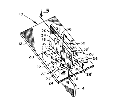
FIG. 1 is an axonometric view of the assembled circuit boards of the
secondary circuit board inserted into the slot of the primary circuit board;
FIG. 2 is a portion of a section view taken along section indicating lines
2-2 of FIG. 1; and,
~14424'~
3 93-CON-157 ~A UJ
FIG. 3 is a portion of a section view taken along section indicating lines
3-3 of FIG. 1.
DETAILED DESCRIPTION
Referring to FIGS. 1 through 3, the assembly of the present invention is
indicated generally at 10 and includes a primary circuit board 12, typically a
printed circuit board, which has an elongated slot 16 formed therein. The
printed circuit board 12 is of the type having a substrate of insulating
material
formed with conductive film thereon portions thereof masked and etched away
to form a desired circuit configuration (not shown. Although not illustrated,
it
will be understood that discrete components may be secured to the board 12
and any circuit thereon.
The opposite elongated sides of the slot 16 have extending therefrom a
plurality of space projections of the substrate material denoted by reference
numeral 18. The ends of the projections 18 on opposite sides of the slot 16
terminate at a closely controlled distance from each other so as to define a
slot
having tightly controlled tolerances on the width of thereof. This distance is
denoted by the reference character "D" in FIG. 3.
The circuit board 12 has a plurality of spaced generally parallel
conductive strips, denoted by reference numerals 20,22,24 in the drawings,
provided on one side of the slot 16. A second plurality of spaced generally
parallel strips denoted by reference numerals 26,28,30 extends on the opposite
side of the slot 16 which strips are formed on the surface of the printed
circuit
board 12 with their ends terminating at the edges of the slot 16 intermediate
the projections 18.
As shown in FIG. 2, if desired each of the strips such as strips
20, 22, 24, 26, 28, 30 on the upper surface of the primary board 12 may have a
counterpart strip located directly below on the undersurface of the board as
denoted by reference numerals 20',22',24',26',28',30' in FIGS. 1 and 2. It
will
be understood however, that the counterpart strips 20',22',24',26',28',30' are
not necessary for the practice of the invention.
The secondary board 14 likewise has a plurality of conductive strips
disposed thereon in spaced generally parallel relationship on the insert
portion of
214424'
4 93-CON-157 (A Ul
the board which is denoted by reference numeral 32 and which strips are
denoted by reference numerals 34,36,38 on the front side of the board portion
32. Preferably counterpart strips denoted with corresponding primed numerals
are provided on the opposite face thereof.
Referring to FIG. 2, the strips on the portion 32 of member 14 are
disposed oppositely in pairs at a common station thereon such as the pair 36,
36' and are interconnected through a hole or "via" aperture 40 formed through
the insulating substrate material which permits the metal conductor when
plated
on the board 14 to be deposited in the "via" aperture and interconnect the
strips 36, 36'. It will be understood that in similar fashion strips 34 and
its
oppositely disposed strip 34' which is shown only in dashed outline are
interconnected, as are strip 38 and its oppositely disposed strip 38' which is
shown only in dashed outline.
Upon insertion of the portion 32 of secondary board 14 into the slot 16,
the lug portions 18 position and maintain the boards 12,14 in mutually
perpendicular arrangement. The strips on the primary board are then
interconnected with the strips respectively disposed adjacent thereto by
soldering as denoted by reference numeral 42, preferably by wave soldering,
which bridges the gaps therebetween and makes electrical contact with the
strips on the secondary board. FIG. 2 illustrates typically the electrical
connection between strip 36 and the strips 22, 22' and the electrical
connection
between strip 36' and the strips 28, 28'. It will be understood that strips
20', 22', 24' and 26', 28', 30' may be omitted and are not essential for the
practice of the invention.
The present invention thus provides for direct plug-in connection of
individual circuit boards by insertion of a portion of one sized and
configured to
closely interfit a slot in the other board with strips provided on each board
terminating closely spaced and adjacent and which are subsequently
electrically
interconnected by soldering.
Although the invention has been described hereinabove with respect to
the illustrated embodiments, it will be understood that the invention is
capable
of modification and variation and is limited only by the following claims.