Note: Descriptions are shown in the official language in which they were submitted.
NE-646 21~4368
,
TITLE OF THE INVENTION
2 "MOS Transconductance Amplifier Having Squaring Circuit for LSI
3 Implementation"
4 BACKGROUND OF THE INVENTION
- 5 Field of the Invention
6 The present invention relates generally to metal oxide
7 semiconductor (MOS) operational transconductance amplifier for
8 providing linear amplification of an analog input voltage to produce an
9 amplified analog output current, and more specifically to a MOS
operational transconductance amplifier suitable for LSI implementation.
11 Description of the Related Art
12 An operational transconductance amplifier is described in a
13 paper "Design of Linear CMOS Transconductance Elements", Nedungadi
14 et al, IEEE Transactions on Circuits and Systems, Vol. CAS-31, No. 10,
October 1984, pages 891-894. The known transconductance amplifier
16 includes four transistors connected in an unbalanced cross-coupled quad
17 cell configuration for supplying a bias current to a MOS differential pair to
18 which an input voltage is applied. To optimize the bias current for linear19 operation of the transconductance amplifier, it is necessary to set the
width-to-length ratio of the channels of the quad cell transistors at
21 1: ( 1 + 2/ ~ ). However, the ratio of this value is impractical for LSI
22 implementation in so far as linear amplification is concerned.
23 SUMMARY OF THE INVENTION
24 It is therefore an object of the present invention to provide a MOS
operational transconductance amplifier which can be implemented using
26 LSI technology.
27 According to a first aspect, the present invention provides a MOS
28 operational transconductance amplifier which comprises a MOS transistor
2 9 differential pair having gate terminals for receiving an input voltage
thereacross and having channels connected together to a common node,
NE-646 ~144368
and a squaring circuit. The squaring circuit comprises first and second
2 constant current sinks connected to a reference potential, a first current
3 mirror connected to a voltage supply, and a second current mirror
4 connected to the reference potential. A third current mirror is connected
- 5 to the voltage supply, and a fourth current mirror is connected to the
6 reference potential, the second and fourth current mirrors being
7 connected together to the common node. The channel of a first MOS
8 transistor is connected between the voltage supply and the first constant
9 current sink, and the channel of a second MOS transistor is connected at
one end to the first current mirror and at the other end to the first constant
11 current sink and the second current mirror. The channel of a third MOS
12 transistor is connected at one end to the third current mirror and at the
13 other end to the second constant current sink and the fourth current
14 mirror, and the channel of a fourth MOS transistor is connected between
the voltage supply and the second constant current sink. The gate
16 terminals of the first and third MOS transistors are coupled together and
17 the gate terminals of the second and fourth MOS transistors are coupled
8 together to receive the input voltage. The first and second current mirrors19 and the second MOS transistor are connected to form a first
bootstrapping loop so that the second current mirror produces at the
21 node a first current equal to a sum of a constant current produced by the
22 first constant current sink and a current equal to a drain current produced
2 3 by one of the first and second MOS transistors. The third and fourth
24 current mirrors and the third MOS transistor are connected to form a
second bootstrapping loop so that the fourth current mirror produces at
26 the node a second current equal to a sum of a constant current produced
27 by the second constant current sink and a current equal to a drain current2 8 produced by one of the third and fourth MOS transistors. The first and
29 second currents are combined together at the node to drive the MOS
3 0 transistor differential pair.
2144368
` NE-646
- 3 -
According to a second aspect, the present invention provides a
2 MOS operational transconductance amplifier comprising a MOS transistor
3 differential pair having gate terminals connected respectively to input
4 terminals for receiving an input voltage thereacross and having channels
connected together to a first node. A first current mirror is connected to a
6 voltage supply, and a second current mirror is connected to a reference
7 potential and a second node connected to the first node. A first MOS
8 transistor has a channel connected between the first current mirror and a
9 constant current sink, and a second MOS transistor has a channel
10 connected at one end to the first current mirror and at the other end to
11 the constant current sink and the second current mirror, the gate terminals
12 of the first and second MOS transistors being connected respectively to
13 the input terminals. First and second resistors of equal value are
14 connected in series between the gate terminals of the first and second
MOS transistors. A third MOS transistor is provided having a channel
16 connected between the voltage supply and the constant current sink, the
17 gate terminal thereof being connected to a node formed between the first
18 and second resistors. The first and second current mirrors and the
19 second MOS transistor are connected to form a bootstrapping loop so
that the second current mirror produces at the second node a current
21 equal to a sum of a constant current produced by the constant current
22 means and a current equal to a drain current produced by one of the first
23 and second MOS transistors.
24 BRIEF DESCRIPTION OF THE DRAWINGS
The present invention will be described in further detail with
26 reference to the accompanying drawings, in which:
27 Fig. 1 is a block diagram of a prior art MOS (metal oxide
28 semiconductor) operational transconductance amplifier;
29 Fig. 2 is a graphic representation of the results of the SPICE
3 0 simulation performed on the prior art transconductance amplifier;
NE-646 21 4 4 3 6 8
- 4 -
Fig. 3 is a schematic block diagram of the MOS operational
2 transconductance amplifier of the present invention;
3 Fig. 4 is a graphic representation of an idealized input-to-output
4 characteristic of the squaring circuit of the present invention;
s Fig. 5A is a circuit diagram of the squaring circuit according to a6 first embodiment of the present invention;
7 Fig. 5B is a circuit diagram of the squaring circuit according to a8 modified form of the present invention in which the output current of the
9 squaring circuit is scaled at 1/4 of the output current of Fig. 5A;
Fig. 5C is a circuit diagram of the squaring circuit according to a
11 third embodiment of the present invention wherein the output current of
12 the squaring circuit is scaled at 1/4 of the output current of Fig. 5A;
13 Fig. 5D is a circuit diagram of the squaring circuit according to a14 further modification of the present invention in which the input voltage of
the squaring circuit is equivalently scaled at 1/2 of the voltage input of the
1 6 MOS differential pair;
17 Fig. 5E is a circuit diagram of the squaring circuit according to a18 still further modification of the present invention in which the input voltage
19 of the squaring circuit is equivalently scaled at 1/2 of the voltage input of
2 0 the MOS differential pair;
21 Fig. 6A is a graphic representation of the input-to-output
22 characteristic of the squaring circuit of Fig. 5A;
23 Fig. 6B is a graphic representation of the input-to-output
24 characteristic of the squaring circuits of Figs. SB, 5C, 5D and SE;
Fig. 7A is a graphic representation of the input-to-output
26 characteristic of the operational transconductance amplifier incorporating27 the squaring circuit of Fig. 5A; and
2 8 Fig. 7B is a graphic representation of the input-to-output
29 characteristic of the operational transconductance amplifier incorporating3 0 the squaring circuits of Figs. 5B, SC, SD and 5E.
NE-646 2144368
- 5 -
DETAILED DESCRIPTION
2 Before proceeding with the detailed description of the present
3 invention, it may prove helpful to provide an explanation of the
4 Nedungadi et al's operational transconductance amplifier with reference
to Fig. 1. The prior art transconductance amplifier includes MOS
6 transistors M18 to M27, wherein the transistors M18 and M19 form a
7 current mirror circuit. The transistors M21 and M24 constitute a first
8 unbalanced differential pair and the transistors M22 and M25 a second
9 unbalanced d;fferential pair, which pairs are connected in a cross-coupledguad cell configuration to operate as a squaring circuit. The output
1 current (tail current) of the squaring circuit is used to drive the transistors
12 M26 and M27 which form a differential pair. By operating the differential
13 pair with an optimum bias, the transistors M26 and M27 operate as a
1 4 linear amplifier for a specified range of input voltages. The transistor
M23 and a current sink 10 are used to level shift the summed drain
16 currents of M21 and M22 from the node A to the node B.
17 The following mathematical analysis of the circuit of Fig. 1 gives a18 tail current for the squaring circuit that is necessary for the differential pair
19 (M26 and M27) to operate as a linear amplifier. It is assumed that
semiconductor elements fabricated on a common chip have excellently
21 matched characteristics and that the effect of channel-length modulation
22 and the body effect are ignored. The relationship between the drain
23 current IDi of a saturated MOS transistor and the gate-source voltage
24 VGSi~ if it follows the square-law, is given by Equations la and 1 b:
2 5 IDi = ,B (VGsi - VTH)2 ~if VGSi > VTH) (la)
2 6 IDi = (if VGSi ~ VTH) (lb)
27 where, VTH jS the threshold voltage and ~ = ,L(CoX/2)(W/L), where ~1 is the
28 effective surface carrier mobility, COx is the gate oxide capacitance per
29 unit area, and W and L are the width and length of the channel,
3 0 respectively. The output current ~ID of the MOS differential pair (M26,
NE-646 214436~
- 6 -
M27) that is driven by a tail current ISS is given Equations (2a) and (2b) as
2 follows:
~Vi~2~ s _ Vi2 (if lVil < ~) (2a)
ISS sgn (Vi) (if ¦Vj¦2~) (2b)
4 Since the tail current lSS is proportional to the square of the input
s voltage, the nonlinearity of the transconductance of the MOS differential
6 pair is completely compensated and therefore the tail current for
7 optimizing the bias for the M26-M27 differential pair is ~iven by:
8 ISS= Io + (1/2)~Vi2 ( )
g As a result, the output current IL f the unbalanced cross-coupled
10 quad cell formed by transistors M21, M24, M22 and M25 is given by
11 Equations (4a), (4b) and (4c) as follows:
12 IL = aI--(ID21 + ID22)
1 3 = aI _ 2nl I + 2 n(n - 1) ~Vi2 ( I i l - ~¦ n~ ) ( )
3n -1 n(n + 1)~Vi2 + 2n~¦Vi¦~ (n + 1)2 ~ - nVi2
14 =aI+ I +
2n+1 (n+1)'
1 5 (if ~(n + l)I < lvil < ~(n +~1)I ) (4b
16 =aI (iflVil2~(n+1)I~ (4c)
17 where ID21 and ID22 are the drain currents of transistors M21 and M22,
18 respectively, and n is the ratio between the two channel's width-to-length
19 ratios (=W/L), i.e., the ratio between the ~-values of these transistors.
Since Equation (4a) must be equal to Equation (3), it is necessary
21 to set the tail current lSS as:
2 2 ISS = aI _ 2nl I + 2 n(n 12) ~Vi2 = Io + 2 ~Vi2 (5)
23 Therefore, the transconductance gm can be held at a constarlt
24 value as given by Equation (6) for an input voltage Vi in the range
NE-646 21443 6~
- 7 -
lVi¦<~l(n+l)I/(n~):
2 gm =~l{a-2nl(n+l))(Il~) - (6)
3 The square terms of Equation (5) are made equal to each other
4 by setting Equation (7) as follows:
s 2n(n - l)/(n + 1)2= 1/~ (7)
6 By solving Equation (7) for n, n = 1 + 2/ ~ (= 2.1547) is obtained.
7 The SPICE simulation undertaken by Nedungadi et al for n = 2, n
8 = 2.1, n = 2.155, n = 2.2 and n = 2.3 indicates that the nonlinear error of
9 transconductance for n = 2.155 is lower than 0.1% (Fig.2).
1 0 However, the n-value of 1 : 1 + 2 / ~ is impractical for LSI
11 implementations in so far as linear amplification is concerned. If this n-12 value is rounded, the bias current cannot be optimized for linear
1 3 amplification.
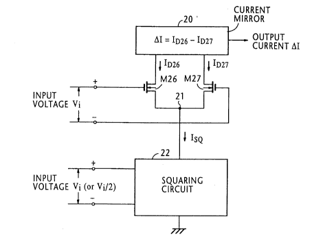
14 Referring now to Fig. 3, the MOS operational transconductance
amplifier of the present invention is schematically illustrated, wherein
16 elements corresponding to those in Fig. 1 are marked with the same
17 reference numerals. The amplifier of this invention comprises a current
18 mirror circuit 20 which is formed by the MOS transistors M18 and M19 of
19 Fig. 1. The drain terminals of MOS transistors M26 and M27 are
2 0 connected to the current mirror circuit 20 and their source terminals
21 coupled together to a node 21 to produce drain currents ID26 and ID27,
22 respectively. The current mirror circuit 20 produces an output current
2 3 equal to the difference between the drain currents ID26 and ID27.
24 According to the present invention, a squaring circuit 22 is
2 5 connected to the MOS differential pair (M26, M27) to drive the transistors2 6 of the differential pair with a tail current IsQ~ The input voltage Vj is
27 supplied to the squaring circuit 22 as well as to the gate terminals of the
2 8 MOS differential pair. The squaring circuit 22 converts the input voltage V
2 9 to the tail current IsQ and an output current ~I is produced, which is
NE-646 2144368
obtained from the current mirror circuit 20.
2 If the MOS differential pair (M26, M27) is driven by a constant
3 current, the input-to-output characteristic of the transconductance
4 amplifier of Fig. 3 will lose its linearity before the input voltage reaches +1
or-1 as indicated by broken lines in Fig. 4. However, the squaring circuit
6 22 provides bias optimization in such a manner that the linear
7 amplification range of the transconductance amplifier extends to + ~ as
8 indicated by a solid-line linearized curve in Fig. 4. The present invention is
g intended to provide a MOS operational transconductance amplifier whose
linear amplification range approximates the linearized curve of Fig. 4.
11 Fig. SA shows details of the squaring circuit 22 according to an
12 embodiment of the present invention. It is seen that the squaring circuit
13 includes a first differential pair 51 formed by MOS transistors M1 and M2,14 and a second differential pair formed by MOS transistors M3 and M4.
The drain terminals of transistors M1 and M4 are directly connected to a
16 volta~e supply VDD. Whereas, the drain terminal of transistor M2 is
17 connected to the VDD supply via a current mirror circuit 53 formed by
18 MOS transistors M5 and M6, and the drain terminal of transistor M3 is
19 connected to the VDD supply via a current mirror circuit 54 formed by
MOS transistors M10 and M11. The source terminals of transistors M1
21 and M2 are coupled together to a constant current sink SS (where current
22 Io is passed to ground) as well as to a current mirror circuit 56 formed by
23 MOS transistors M7, M8 and M9. In like manner, the source terminals of
24 transistors M3 and M4 are coupled together to a constant current sink 57
2 5 as well as to a current mirror circuit 58 formed by MOS transistors M12,
2 6 M13 and M14. Transistors M1, M2, MS to M9 constitute a first differential
27 circuit and transistors M3, M4, M10 to M14 constitute a second differential
2 8 circuit and the output of each of these differential circuits is connected to
2 9 the output of the other differential circuit at a node 62.
3 0 A first bootstrapping loop 60 is formed by transistors M2, MS,
NE-646 2144368
g
M6, M7 and M8 by coupling the drain-source paths of transistors M2 and
2 M7 in series between transistor MS and ground and coupling the drain-
3 source path of transistor M8 between transistor M6 and ground. A
4 second bootstrapping loop 61is likewise formed by transistors M3, M10,
S Mll, M12 and M13 by coupling the drain-source paths of transistors M3
6 and M12 in series between transistor M10 and ground and coupling the
7 drain-source path of transistor M13 between transistor M11 and ground.
8 Transistors M9 and M14 have their drain terminals connected together to
g the node 62 which leads to the node 21 to draw tail current IsQ and have
10 their gate terminals coupled to the drain terminals of transistors M8 and
11 M13, respectively.
12 The gate terminals of transistors Ml and M3 are coupled
13 together to a positive voltage input terminal 63 and the gate terminals of
14 transistors M2 and M4 are coupled together to a negative voltage input
15 terminal 64. The input voltage Vj is applied across the terminals 63 and
16 64,so that transistors Ml and M3 are driven together in opposite sense to
17 transistors M2 and M4. Due to the bootstrapping loop 60, the second
18 current mirror circuit 56 produces at the node 62 a first current equal to a
19 sum of a constant current Io produced by the constant current sink SS and
20 a current equal to the drain current of one of the MOS transistors M1 and
21 M2. Likewise, due-to the bootstrapping loop 61, the fourth current mirror
22 circuit 58 produces at the node 62 a second current equal to a sum of a
23 constant current Io produced by the second constant current sink 57 and a
24 current equal to the drain current of one of the MOS transistors M3 and
25 M4. As a result, transistors M2 and M3 are driven by drain currents
26 (dynamic bias currents) ID2 and ID3~ respectively, which are given by:
2 7 ID2 = ~(Vi--~) (if V~ ) (8a)
2 8 ID2 = (if Vi > ~) (8b)
NE-646 21443 68
- 10-
ID3 =~(--Vi--~) (if Vi <~) (8c)
2 ID3 = (if Vi ~ ~) (8d)
3 It is seen that each of these dynamic bias currents exhibits the
4 square-law characteristic. Each of the Equations (8a) and (8c) is
equivalent to Equation (1 a) in the sense that VSGi and VTH of Equation
6 (1 a) are substituted by Vi and ~, respectively. It is appreciated that
7 Equations (8a) and (8c) are represented by such physical parameters
8 which can be implemented by a computer program. Thus, the squaring
9 circuit of this invention can be implemented on LSI chips.
The tail current ISQ jS obtained by summing the dynamic bias
11 currents ID2 and ID3 as follows:
1 2 ISQ = ID2 + ID3
1 3 = 2~Vi2 + 2Io (if lVil < ~) (9a)
14 = ~(Vi+~)2 (iflVil2~) (9b~
Fig. 6A is a graphic representation of the input-to-output
16 characteristic of the squaring circuit 22 of Fig. SA given by Equations (9a)
17 and (9b). Fig. 6A indicates that by using the square-law characteristic of
18 the MOS transistor an ideal square-law characteristic can be obtained for
19 a transconductance ampiifier for a range between - 1 volt and +1 volt of
normalized input voltage. This range is wider than any of the ranges
21 attainable with prior art transconductance amplifiers.
2 2 In relation to the tail current ISS given by Equation (3) it is seen2 3 that the tail current ISQ must be scaled by a factor 1/4 or the input voltage
24 Vi of the squaring circuit 22 must be scaled by a factor 1/2.
As illustrated in Fig. SB, the tail current ISQ can be divided by 4 by
2 6 setting, in each of the current mirror circuits 56 and 58, the width-to-
2 7 length ratios (or ~-values) of the transistors M7, M8, M1 2 and M1 3
21~3~8
NE-646
- 1 1 -
provided on the side of the differential pairs (transistors M1, M2, M3, M4)
2 at a value four times higher than the width-to-length ratio of the
3 transistors M9 and M14 which are provided on the output side of these
4 current mirror circuits. The ~-values of the other MOS transistors of the
squaring circuit are suitably set at an equal value.
6 Alternatively, the tail current IsQ can be divided by 4 by the7 provision of a set of four MOS transistors Ma, Mb, Mc and Md as
8 illustrated in Fig. 5C. These transistors have their gate terminals coupled
9 together to a common bias source VB and their sources coupled together
to the node 62. The node 62 is connected to the node 21 via the source-
11 drain path of transistor Ma, while the drain terminals of transistors Mb, Mc
12 and Md are coupled together to the voltage supply VDD.
13 By scaling the tail current IsQ by a factor 1/4 in a manner
14 mentioned above, the MOS differential pair (M26 and M27) linearly
operates in the + 1 normalized voltages as indicated by the input-to-
16 output curve of Fig. 7A.
17 The input voltage can be divided by 2 by setting the input
18 voltage Vi at one-half of the voltage input to the MOS differential pair
19 (M26, M27) or setting the width-to-length ratios (= ,~-values) of the
transistors M26 and M27 of the MOS differential pair at a value four times
21 higher than the width-to-length ratio of the channels of the transistors M1
22 to M4 as illustrated in Fig. 5D.
23 According to an interesting feature of the present invention, the
24 input voltage can be scaled by a factor 1/2 to advantage by configuring
2 S the squaring circuit 22 of Fig. 5A into simplified circuitry as shown in Fig.
26 5E. The simplified squaring circuit is formed by a single differential circuit
27 which is generally similar to the first differential circuit of Fig. 5A with the
28 exception the drain terminals of MOS transistors M1 and M2 are coupled
29 together and passed through the source-drain path of MOS transistor M5
2144368
NE-646
to the voltage supply VDD, and their gate terminals are coupled by series-
2 connected resistors 70 and 71 of equal value. A MOS transistor Me is
3 provided so that its drain-source path is connected between the voltage
4 supply VDD and the constant current sink 55 as well as to the drain
5 terminal of transistor M7, the gate terminal of transistor Me being
6 connected to the node between resistors 70 and 71. According to this
7 simplified configuration, the tail current IsQ is given by Equation (10) as
8 follows:
9 IsQ = 1,13Vi2+2Io (if lVil<2~) (10)
As shown in Fig. 6B, the range of linear amplification of the
11 squaring circuits of Figs. SB, SC, SD and SE is extended over a range
12 which is twice the range of Fig. 6A. In a similar manner, the linear
13 amplification range of the MOS differential pair can be extended twice the
14 range of Fig. 7A by the squaring circuits of Figs. 5B, SC, 5D and SE as
15 shown in Fig. 7B.
16 Another important characteristic of the MOS operational
17 transconductance amplifier of this invention is that it can be operated at
1 8 low voltages.
19 The foregoing description shows only preferred embodiments of
20 the present invention. Various modifications are apparent to those skilled in
21 the art without departing from the scope of the present invention which is
22 only limited by the appended claims. Therefore, the embodiments shown
23 and described are only illustrative, not restrictive.