Note: Descriptions are shown in the official language in which they were submitted.
2~4~~?'~
-1-
A Luminance Weighted Discrete Level Display
Field of the Invention
The present invention relates to a colour display apparatus such as colour
computer displays and colour printers, and, in particular, to the display of
colour
images on a raster colour display apparatus.
The background of the invention will now be described with reference to the
following drawings in which:
Fig. 1 is a schematic view of a conventional single pixel of a CRT type
~ o display.
Referring now to Fig. 1, there is shown a single pixel 1 of a normal Cathode
Ray Tube (CRT) type display device. Each pixel is made up of a Red 2, Green 3
and
Blue 4 phosphor dot or pixel elements. These dots are so small that when
grouped
together with a large number of other pixels, the light emanating from the
individual
~ s dots is perceived by the viewer as a mixture of the corresponding three
colours. A wide
range of different colours can thus be produced by a pixel element by
variation of the
strength with which each phosphor dot is excited.
The display of colour images in these devices is normally achieved by storing
an associated value for each pixel of the display and sending this value to an
intensity
2o conversion means with the display at the requisite time. The number of
different
possible values stored for each pixel element of a pixel corresponds with the
number of
different colours which may be displayed by the display device and hence the
resolution
with which the device can display a given picture. With a television signal, a
similar
procedure is adopted of sending a pixel value to the screen corresponding to a
required
zs illumination of each particular pixel. Such procedures are well known by
those skilled
in the art.
By way of example, a 24 bits per pixel colour display system divided into 8
bits for each of the three colours red, green and blue will be assumed. This
corresponds
to 2g or 256 separate intensity levels of each red, green and blue
respectively, giving
so 224 different colour values. A colour display capable of displaying this
many colours
can approximate a continuous tone image to such a degree that for all
practical purposes
the display can be considered to be a continuous tone display.
Colours are often displayed on a computer display according to a particular
model. The red, green, blue (RGB) colour model is one that is in common use
with
35 CRT and colour raster display devices. Other colour display models include
cyan,
magenta, yellow (CMS often used in colour-printing devices. An example of the
RGB
model is the NTSC picture display standard in common use with computer
displays.
As the intensity of each phosphor dot can be varied in an analogue manner, the
optical centre of the illumination from the phosphor dot is the centre of that
dot
[N:\LIBE]MACR002:LDP
2I4~44?'~
_2_
regardless of the light intensity produced. Additionally, when multiple
primary pixel
elements are used to display a given colour, the perceived optical centre of
the
illumination remains substantially in the same place. Effectively, the
position of a pixel
is at its optical centre of illumination and, as such, all images displayed on
a
workstation CRT assume that the optical centres of pixel are in a regular
rectangular
grid.
Many display devices are unable to actually display the full range of colours
provided by, for example, a 24 bit input pixel. For example, a black and white
raster
image display can only display 2 colours, namely black and white and is known
as a bi-
i o level device. Other colour display devices can only display a finite
number of discrete
intensity levels for each colour unit. By way of further example, in a colour
bi-level
device, such as a bilevel ferro-electric liquid crystal display (FLCD), each
illumination
area on the screen can be at just two intensity levels, either fully on or
fully off.
If the display device receives an input which has been generated on the basis
15 that each pixel is able to display a larger number of intensity levels than
can actually be
displayed, then there will be an error in the colour displayed, being the
difference
between the exact pixel value required to be displayed and the approximated
value
actually displayed.
Methods of generating input signals to discrete type displays have been
Zo developed to increase the number of apparent colours displayable on an
discrete colour
display device such as a bi-level colour display. The methods used are known
generally
as halftoning. For an explanation of the different aspects of halftoning the
reader is
referred to a standard textbook such as 'Digital Halftoning' by Report
Ulichney,
published in 1991 by MIT Press.
25 The present invention is applicable to many different types of discrete
level
displays including plasma displays, electro-luminescent displays and ferro-
electric
displays. The present invention is further applicable to displays having a
number of
discrete illumination areas with each area being capable of being illuminated
to one or
more levels.
so The preferred embodiment of the present invention will be described in
relation to a particular configuration of a FLCD display. In the design of a
particular
FLCD display in which each pixel is made up of a number of areas which can be
independently illuminated, a number of constraints or trade-offs must be
enforced. On
the one hand, it is desired to maximise the illumination properties of a
particular panel
ss while keeping the design of the panel as simple as possible in order to
ensure that it can
be readily manufactured. Further constraints include a general need to limit
the number
of opaque drive lines available for driving the areas of a pixel which can be
independently illuminated, and the need to faithfully reproduce the desired
image with
as little distortion as possible.
fN:\LIBE1MACH002:LDP
21444'9
-3-
In order to increase the number of possible intensity levels per pixel group
methods of utilizing varying size sub-pixels have been developed. For example,
United
States Patent 5,124,695 (Green / Thorn EMI) discloses a pixel pattern
arrangement
where sub-pixels of varying size are used in relation to monochrome displays.
The use
of sub-pixels of varying size is also disclosed in European Patent Application
361,981
(Nakagawa et. al. / Sharp).
Summary of the Invention
It is a general object of the present invention to produce an improved form of
colour discrete level display in comparison with that disclosed by the prior
art.
~ o In accordance with a first aspect of the invention there is provided a
method
for determining a pixel layout pattern for a display having a plurality of
pixels, each
said pixel having a plurality of independently illuminable areas, each said
area being
assigned to one of a plurality of primary colour components, said method
comprising at
least the step of allocating said independently illuminated areas to said
primary colour
~ s components in a ratio such that the condition of the illuminated areas to
one colour
component is different from that of the illuminated areas to the other colour
component.
In accordance with a second aspect of the invention there is provided a method
for determining the number of drive lines allocated to each primary colour of
a discrete
level colour display, said display having a plurality of pixels, each said
pixel having a
2o plurality of independently illuminable area , each said area being assigned
to one of a
plurality of primary colour components, said method comprising at least the
step of
allocating said drive lines to said primary colour in a ratio such that the
condition of the
illuminated areas to one colour component is different from that of the
illuminated areas
to the other colour component.
is In accordance with a third aspect of the invention there is provided a
colour
display apparatus having a plurality of independently illuminable areas each
of which is
assigned to one of a plurality of primary colour components, wherein said
independently illuminated areas are allocated to said primary colour
components in a
ratio such that the condition of the illuminated areas to one colour component
is
so different from that of the illuminated areas to the other colour component.
In accordance with a fourth aspect of the invention there is provided a colour
display apparatus having a first plurality of independently illuminable areas
connected
to second plurality of data drive lines, each of said illuminable areas being
assigned to
one of a plurality of primary colour components, wherein said data drive lines
are
as allocated to said primary colour components in a ratio such that the
condition of the
illuminated areas to one colour component is different from that of the
illuminated areas
to the other colour component.
[N:\LIBE]MACR002:LDP
21444'9
-4-
A preferred embodiment of the present invention will now be described with
reference to the accompanying drawings in which:
Fig. 2 illustrates a graph of the relative sensitivity of the eye;
Fig. 3 illustrates a graph of the relative responses of the eye to the red,
green
s and blue primary colours;
Fig. 4 is a simplified plan view of a pixel arrangement not having the
attributes
of the present invention;
Fig. 5 illustrates the levels of the primary colours of a display such as that
shown in Fig. 4;
~ o Fig. 6 illustrates the discrete threshold error of a primary colour of the
display
as shown in Fig. 4;
Fig. 7 illustrates the discrete threshold error comparison for the primary
colour
of a display having an increased number of drive lines;
Fig. 8 is a plan view of the pixel configuration employing the preferred
i s embodiment of the present invention;
Fig. 9 illustrates the levels of the primary colours of the pixel
configuration as
shown in Fig. 8;
Fig. 10 illustrates the basic operation of a ferro-electric liquid crystal
display
device;
2o Fig. 11 is a cross section taken through the line A-A of Fig. 8;
Fig. 12 is a cross section, similar to Fig. 11, but illustrating the
construction of
the data metal layer of a pixel;
Fig. 13 illustrates the data metal mask utilised in construction of the data
metal
layer of Fig. 12;
zs Fig. 14 is a cross section, illustrating the construction of the data level
transparent layer of the preferred embodiment;
Fig. 15 illustrates the pixel mask utilising the construction of the
transparent
layer of Fig. 14;
Fig. 16 is a cross section illustrating the construction of a surface layer of
the
so top substrate;
Fig. 17 is a cross section illustrating the formation of the common level
metal
layer on a bottom substrate;
Fig. 18 illustrates the pixel mask utilised in the construction of the common
metal layer of Fig. 17;
35 Fig. 19 is a cross section illustrating the construction of the common
level
transparent layer on the bottom substrate;
Fig. 20 illustrates the pixel mask utilised in construction of the common
level
transparent layer of Fig. 19;
[N:\LIBE1MACR002:LDP
21444 ~g
-5-
Fig. 21 is a cross section illustrating the formation of the common level
surface layer on the bottom substrate;
Fig. 22 is a cross section of a pixel of a display taken through the line A-A
of
Fig. 8; and
Fig. 23 illustrates, partly in section, the layout of a number of pixels of a
liquid crystal type display, in accordance with the preferred embodiment.
Description of the Preferred Embodiment
In accordance with a first embodiment of the present invention there is
provided a method for determining a pixel layout pattern for a display having
a
~ o plurality of pixels, each pixel having a plurality of independently
illuminable areas,
each area being assigned to one of a plurality of primary colour components,
each
primary colour component having a corresponding human eye response function,
said
method comprising allocating said independently illuminated areas to said
primary
colour components in a ratio substantially in accordance with the ratio of
said
~ 5 corresponding human eye response functions.
In accordance with a second embodiment of the present invention there is
provided a method for determining the number of drive lines allocated to each
primary
colour of a discrete level colour display, said display having a plurality of
pixels, each
pixel having a plurality of independently illuminable areas, each area being
assigned to
20 one of a plurality of primary colour components, each primary colour
component
having a corresponding human eye response function, said method comprising
allocating said drive lines to said primary colours in a ratio substantially
in accordance
with the logarithmic ratio of said corresponding human eye response functions.
In accordance with a third embodiment of the present invention there is
25 provided a colour display having a plurality of independently illuminable
areas each of
which is assigned to one of a plurality of primary colour components, each of
said
primary colour components having a corresponding human eye response function,
wherein said independently illuminated areas are allocated to said primary
colour
components in a ratio substantially in accordance with the ratio of said
corresponding
so human eye response function.
In accordance with a fourth embodiment of the present invention there is
provided a colour display having a first plurality of independently
illuminable areas
connected to second plurality of data drive lines, each of said illuminable~
areas being
assigned to one of a plurality of primary colour components, each of said
primary
a5 colour components having a corresponding human eye response function,
wherein said
data drive lines are allocated to said primary colour components in a ratio
substantially
in accordance with the logarithmic ratio of said corresponding human eye
response
function.
[N:\LIBE1MACR002:LDP
214 44'9
-6-
The human eye is not uniformly sensitive over the visible spectrum and as such
the eye is more sensitive to some displayed colours than to other displayed
colours.
This can be seen in Fig. 2 which shows the relative average response of the
human eye
to light of constant luminance projected at various wavelengths throughout the
spectrum. The sensitivity curve peaks in the yellow-green region 8 indicating
that the
eye is a lot more sensitive to yellow-green than any other colours.
Almost all colours required to be created can be achieved by mixing the three
primary colours red, green and blue in various proportions. This principle is
closely
followed by the eye, where there are believed to be only three types of cones
or
~ o receptors correlating closely to red, green and blue, and each type of
cone has a
different response curve. Referring now to Fig. 3, the response curves of the
relative
sensitivities of the eye to the three primary colours, red 5, green 6, and
blue 7 are
shown as well as the total response curve 8. The curves overlap in such a way
that all
spectral colours are beneath either only one, or else partly under two of the
three
~ s curves. As can be seen from Fig. 3, the eye has greater sensitivity to
green than to red
or blue, and greater sensitivity to red than blue.
Referring now to Fig. 4 there is shown a pixel design for an arrangement in a
first form of conventional display 29. In this particular arrangement, the
number of
areas or pixel sub-elements that can be independently illuminated (eg., 9, 10,
11) and
2o the number of drive lines allocated to each of the three primary colours
red, green and
blue are treated equally in a conventional fashion. Hence there are six sub-
elements per
pixel and two binary weighted sub-elements are assigned to each primary colour
thus
achieving four possible levels of output for each primary colour as shown in
Fig. 5. It
should be noted that arrangement 29 of Fig. 4, by treating each primary colour
equally,
2s does not take into account the weighted response of the human eye to each
colour's
illumination.
Referring now to Fig. 6, there is illustrated an example of the error 15 which
can be produced when displaying an image on a discrete level display with four
possible levels. This error comprises the difference between an arbitrary
level 13 which
ao is desired to be displayed and the closest corresponding displayable level
14. Of course,
the error 15 increases significantly when there are only a limited number of
intensity
levels which can be displayed by the pixel.
The number of individual possible displayable levels can be made to increase
exponentially with the number of available drive lines. Fig. 7 illustrates the
situation
as where the number of drive lines devoted to each primary colour is increased
to three. In
this case the number of possible intensity levels will be increased to eight
when the
illumination of each displayable area of a primary colour forms a binary
relationship. In
this case, the maximum error 16 is substantially reduced.
[N:\LIBEJMACR002:LDP
. 244479
_, _
The preferred embodiment of the present invention minimises the maximum
error as seen by the eye, by applying the weighted response of the eye to the
amount of
levels allocated to each primary colour and hence to the number of drive lines
allocated
to each primary colour.
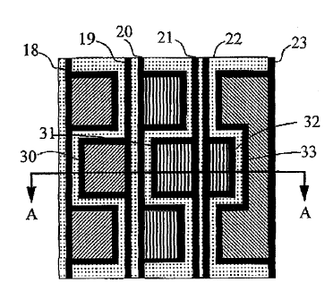
s Referring now to Fig. 8, there is shown the preferred embodiment of the
present invention for a pixel layout for a display having six drive lines,
divided into
two red drive lines 18, 19, three green drive lines 20, 21, 22 and one blue
drive line
23. The pixel layout is suitable for utilisation with many different types of
displays
including FLCD displays.
~ o The eye, being most sensitive to green, will pick up the error due to the
discrete nature of the green sub-pixels more readily than the other two
primary colours.
For blue colours, the errors are less noticeable since the eye is not as
sensitive to blue
when compared to green or red. Therefore, in the present embodiment, more
drive
lines are devoted to green, a lesser number of drive lines are devoted to red,
and even
~ s fewer drive lines are devoted to blue.
The green colour, in the preferred embodiment has more subpixels and, as
such, will have more discrete levels per pixel. This has the effect of
reducing the
threshold error for green. As seen before, Fig. 7 illustrates this concept
where 16 is the
maximum error. However, to increase the number of levels of green, the number
of
20 levels of blue were decreased thus the error for blue is increased. It has
surprisingly
been found that a decrease in the number of blue levels does not have a very
significant
effect on the overall appearance of the displayed image as the eye is not as
sensitive to
blue as it is to green.
In order to determine the number of address lines to be assigned to each
Zs primary colour, a choice approximating the ratio of the eye's response to
the individual
colours can be made.
Alternatively, a more quantitative measure of assignment can be obtained by
examining the luminance weighted threshold error and deriving a formula for
halftoning
distortion as a function of the distribution of bits between the different
colours in a
so pixel.
In order to derive this formula, a number of assumptions have to be made. It
is
assumed that the distortion perceived by the eye which is due to halftoning of
an image
in one colour is proportional to the variance about a mean intensity level
that is
displayed. It is further assumed that distortion perceived for a full colour
image is the
as sum of perceived distortions from the three colour components of that
image, and that
the distortion in each colour is independent of distortion in other colours.
It is further
assumed that different primary colours give different perceived distortion for
the same
intensity of distortion. The measure of quality for a pixel is assumed to be
the average
[N:\LIBE]MACR002:LDP
. . 21444'~~
distortion over all colour intensity combinations, with the assumption that
all possible
intensities occur with equal frequency.
From these assumptions, there can first be derived an average perceived
distortion for a pixel:
6 perceived - average perceived distortion for a pixel
__ 2 2 2 2 2 2
w redo av red + w greener av green + w blue6 av blue
(EQ 1)
where
wcolour = contribution of colour noise to perceived noise
6 colour - average perceived distortion in a single colour
~o therefore:
Intensity - Mean)2
6 2 -_ pixels
perceived ~ number of pixels
all intensities
(EQ 2)
The weights wcolour can be naively chosen as the contribution of each colour
to
luminance or alternatively a description of the colour-dependent low-pass
characteristic
~ 5 of the eye can be used. The following luminance equation expresses the
approximate
weightings of the three colour television primaries used in the National
Television
Systems Committee (NTSC) standard, which are necessary to produce one lumen of
white light:
1 lm of white = 0.30 lin of red + 0.59 lm of green + 0.11 lm of blue
Zo (EQ 3)
Note that these values are correct only for the NTSC primary chromaticities
and a white point and, as a result, they are not exactly correct for most
modern RGB
monitors. As the variations in weightings for various modern RGB devices is
likely to
be small, the above mentioned weightings will be used in subsequent
calculations.
25 The next step is to derive an expression for a2colour as a function of
pixel
parameters.
Define
Bcolour = n~~r of bits devoted to the colour
[N:\LIBE1MACR002:LDP
21444 ~g
_9_
(EQ 4)
Assuming the pixel contains binary weighted pixel sub-potions each of which
are separately illuminable, then the number of possible intensity levels which
the pixel
can display increases exponentially with the number of bits or drive lines,
and the
s difference between adjacent possible intensity levels decreases
exponentially with the
number of bits. Therefore if
Lcolour = number of levels = 2B
and
hcolour = distance between levels = 1 -_ 1
L colour -1 2B -1
i o (EQ 5)
then a2colour is a function of the number of bits used for the colour; thus it
is
more properly written as a2colour(Bcolour) ~ Assuming the behaviour of the
noise
between adjacent colours of a multi-level pixel is the same as that for a
single-level
pixel, except for scaling by a factor hcolour it is possible to write:
6 colour ~Bcolour~ = h olour ~Bcolour~ ~ 6 colour ~1~
(EQ 6)
where
a2colour(1) is the average for all intensities of the halftoning noise for
each
intensity. ie:
1
zo 6 colour ~1~ - ~ 6 colour ~l° I ~ dl
I=0
(EQ ~)
[N:1LIBE]MACR002:LDP
. 2I444'~9
- 10-
The halftoning noise for a single intensity is
a colour ~l' I~= ~ (frequency of intensity (intensity - mean intensity~2
(EQ g)
For intensity 1, a reasonable halftoning algorithm should turn on the pixel
with
s frequency I, and turn off the pixel with frequency (1 - I). Assuming that
this is the
case, the mean intensity will be 1, so therefore:
a colour l ~l' I~ = I~l -1~2 + (1- I~ ~0 -1~2
=1(1- I)
(EQ 9)
Substituting Equation 9 into Equation 7 yields
1
a colour~l~= f l~l-I~dl
I=0
_1
6
(EQ 10)
Substituting Equation 10 and Equation 5 into Equation 6 yields
1 1
a colour ~B colour) = 6 12
(2Bcolour -l l
(EQ 11 )
~ s Finally, substituting Equation 11 into Equation 1 yields the final result
2 w2 2
2 __ 1 cared green wblue
6 perceived 6 2 + 2 + 2
(2Bred - 1) C2Bgreen _ 11 (2Bblue _ 1)
(EQ 12)
A pixel binary weighted arrangement as shown in Fig. 4 has equal weightings
for red, green and blue, with each colour having two subpixels. Substituting
2o Bcolour =2 and the weightings mentioned earlier into Equation 10, the
result is that:
~'2perceived =0~~834.
(EQ 13)
(N:\LIBE]MACR002:LDP
21444'~g
-11-
For the preferred embodiment each primary colour has a different number of
subpixels, with Bred=2~ Bgreen=3~ and Bblue=1 ~e weightings stay the same.
Substituting in the result obtained is:
62perceived =0.00487.
(EQ 14)
which results in a reduction in the average perceived distortion for the
pixel.
As is known to those skilled in the art, the construction of discrete level
displays such as a display utilising a chiral smectic liquid crystal or a FLCD
display can
take many different forms depending on the manufacturing technologies used.
~ o Referring now to Fig. 10, there is illustrated the basic operation of a
ferro-
electric liquid crystal display device (FLCD) 40 which comprises a pair of
electrode
plates 41, 42, normally comprising glass substrates coated with a transparent
form of
electrodes, associated electrical supply rails and colour filters. A layer of
liquid crystal
having molecular layers 43 is disposed between and perpendicular or
approximately
~ s perpendicular to the electrode plates. The liquid crystal assumes a chiral
smectic C
phase or an H phase and is disposed in a thickness thin enough (eg: 0.5 - 5
microns) to
release the helical structure inherent to the chiral smectic phase.
When an electric field E (or -E) 44 exceeding a certain threshold is applied
between the upper and lower substrates 41, 42 liquid crystal molecules 43 are
oriented
Zo in accordance with the electric field. A liquid crystal molecule has an
elongated shape
and shows a refractive anisotropy between the long axis and the short axis.
Therefore if
the ferro-electric liquid crystal device 40 is sandwiched between a pair of
crossed
polarisers (not shown) mounted on the glass substrates 41, 42, there will be
provided a
liquid crystal light modulation device.
2s When an electric field 44 exceeding a certain threshold is applied, the
liquid
crystal molecules 43 are oriented to a first polarisation orientation state
45. Further,
when a reverse electric field (-E) is applied, the liquid crystal molecules 43
are oriented
to a second polarisation orientation state 46. These orientation states are
further
retained as long as the electric field which is applied, does not exceed a
certain
so threshold in the reverse direction.
The manufacturing processes utilised in the display construction are very
similar to those used in the construction or fabrication of Very Large Scale
Integrated
Circuit Devices (VLSI) and familiarity with the constructions of such devices
is
assumed.
35 The construction of a FLCD display begins with the two glass substrates.
Referring initially to Fig. 11, an example of the construction of the top
glass substrate
42 will now be described.
[N:\LIBE]MACR002:LDP
21444~~
-12-
After the surface of the substrate 42 has been thoroughly cleaned, an
aluminium chelate coupling agent (not shown) can be applied to ensure the
proper
adhesion to the glass of subsequent layers to the glass substrate.
A spin coating process is then used to apply a 1.5pm layer of photosensitive
polyamide containing a primary colour die, which in the first case will be
red. To
remove residual solvents, the polyamide is pre-baked for approximately 10
minutes at
80°C. The photosensitive polyamide is then exposed using a pixel mask
corresponding
to the area of the red colour filter 51 to be exposed. The polyamide layer is
then
i o developed leaving the red colour filter portions 51 of each pixel on the
substrate 42.
This first colour filter portion 51 is then post baked to form a stable
structure before the
process is repeated for the green filter 52 and blue filter 53. Importantly,
the green
filter 52 is of a larger magnitude than the blue filter 53 as is in accordance
with the
cross section of Fig. 11 which is taken through the line A-A in Fig. 8.
Optionally, a
i s shielding member, such as opaque metal member (not shown) may be disposed
between
neighbouring colour filter portions in order to shield light passing
therethrough.
Referring now to Fig. 12 the next portion of the display device constructed is
preferably the data level metal layer including drive lines 18-23 and
encircling portions
zo 30-33. The deposition of this metal layer occurs directly over the colour
filters.
In the construction of devices using metal layers, the use of Molybdenum (Mo)
has been preferred for the formation of the relevant circuitry. Molybdenum is
preferred
due to its superior patterning properties and planarisation properties.
Aluminium is also a possible candidate for use in patterning of the metal
layer.
zs The resistivity of aluminium is 0.027 ~,S2m at 25°C, whereas the
resistivity of
molybdenum is 0.0547 pS2m at 25°C. Hence a metal conductive layer made
of
aluminium is almost twice as conductive as one made of molybdenum. However,
hillock or spike formation in aluminium, as a result of stress release during
differential
thermal expansion of aluminium in comparison with other substances used in the
ao creation of the display, creates a serious problem with prior forms of
displays which
currently prevents the use of aluminium.
The deposition of a metal layer is well known to those skilled in the art of
semiconductor circuit fabrication and an example process for such deposition
will now
be described.
35 A 0.3pm layer of a Aluminium and 0.5 % Copper (AICu) alloy is first
sputtered onto the surface of the substrate. Preferably the aluminium is
planarised to a
0.09~,m surface height difference. The sputtered aluminium layer is then
primed for
photoresist adhesion by spin coating a monolayer of hexamethyldisilazane
(HMDS). A
l~,m layer of positive photoresist such as AZ1370 is then spin coated on top
of the
[N:\LIBEIMACR002:LDP
2144479
-13-
priming layer. The photoresist is then pre-baked for 3 minutes at 90°C
using an infra-
red oven. The photoresist is then exposed using the pixel mask shown in Fig.
13, which
comprises simple vertical stripes 18-23 corresponding to the various areas of
the data
metal layer and encircling portions eg. 30-33. The photoresist is exposed to
the metal
s mask at 35mJ/cm2.
The photoresist can then be developed for 50 seconds at 23°C in 25%
aqueous
solution AZ-351 and 40 % aqueous solution AZ-311. A development inspection can
then take place before the resist is stripped and any out of tolerance panels
are either
discarded or reworked. The photoresist can then be post-baked at 150° C
before the
~ o sputtered aluminium is wet etched in an agitated solution of 80 %
phosphoric acid, 5
nitric acid, 5 % acetic acid and 10% water at 40°C for 2 minutes.
Finally the remaining photoresist is stripped using a low phenol organic
stripper such as Shipley remover "1112A", leaving the data level metal layer
on the
bottom substrate 42.
~ s Data_ Level Transparent Electrode L.a_y~r
Referring now to Fig. 14, the next layer deposited is the data level
transparent
electrode layer including portions 60-63, with portion 60 forming a red
transparent
electrode, portions 61, 62 forming binary weighted green transparent
electrodes, and
portion 63 forming a blue transparent electrode.
2o This layer is formed by applying a transparent electrode such as ITO
(Indium
Tin Oxide) on the substrate 42.
The process of formation of the data level dielectric layer includes the
sputtering of indium and tin in an oxygenated atmosphere to initially form a
0.07~.m
layer of ITO. This layer of ITO is then primed, again by spin coating a
monolayer of
is HMDS. On top of this layer is spin coated a l~,m layer of positive
photoresist such as
AZ1370. The photoresist can then be pre-baked, to remove solvents, for
approximately
3 minutes at 90°C using an infra-red oven.
The photoresist is then exposed to the data level electrode mask 65 as shown
in
Fig. 15 at an energy of approximately 35mJ/cm2. The photoresist is developed
for 50
3o seconds at 23°C in a 25 % aqueous solution AZ-351 and a 40 % aqueous
solution
AZ311. The photoresist is then post baked at 120°C. The ITO is then wet
etched and
the remaining photoresist is stripped using a low phenol organic stripper such
as
Shipley 'Remover 1112A' leaving the data transparent electrode layer connected
to the
data metal layer.
35 Referring now to Fig. 16, the final step in the construction of the top
substrate
is to apply a surface layer 67. The surface layer includes the sputtering of
0.1 ~.m of a
tantalum pentoxide insulator, the application of O.l~cm of silicon titanium
oxide, the
spin coating of 0.02~,m of polyamide which is then post baked and the surface
subjected
(N:1L18E]MACR002:LDP
21444'9
- 14-
to uniaxial alignment treatment such as rubbing for the proper liquid crystal
molecule
alignment.
The second substrate 41 (Fig. 10) is laid out substantially in the same manner
as the first substrate but for different masks being used.
s Referring now to Fig. 17, the common level metal layer 24 is formed first on
the bottom substrate 41 utilising the same techniques as those discussed in
relation to
the data level metal layer of Fig. 12. The pixel mask utilized in the
construction of
common metal layer 24 is as shown in Fig. 18.
Turning now to Fig. 19, the next step in the construction of the bottom
~ o substrate 41 is the common level transparent layer 25 comprising indium
tin oxide
(ITO) or the like, laid down in accordance with the procedure outlined above
with
reference to Fig. 12. The mask utilized in forming the common level
transparent layer
25 is as shown in Fig. 20. Finally, with reference to Fig. 21, a common level
surface
layer 68 is formed on the common substrate using the techniques outlined above
with
~ s reference to Fig. 16.
Referring now to Fig. 22, there is shown the final form of construction of the
display device 40, which includes the top substrate 42 and bottom substrate 41
each of
which has its surface covered with a polarizing sheet 70, 71, which, depending
on the
desired driving requirement, may have their polarizing axes at right angles to
or
zo parallel to each other. The two substrates 41, 42 are kept apart in a
stable equilibrium
by 1.5 p,m glass spheres 73 which are sprayed on at a density of approximately
100
spheres per square millimetre. The substrates are further held together by
adhesive
drops 74. The adhesive droplets 74 and spheres 73 act to maintain the display
panel 40
in a static equilibrium with the thickness of the layer between the two
substrates 41, 42
2s being of the order of 1.5 p.m, being a diameter of the spheres 73. The
liquid crystal
(not shown) is placed between the two substrates so as to form a ferro-
electric liquid
crystal device.
Referring now to Fig. 23, there is shown, for illustrative purposes, a
sectional
plan view of the overlay between the common layer, comprising common metal
layer
ao 24 and common transparent layer 25. A data level layer, comprising data
metal layer
26 and data transparent layer 27 is also shown. Each column of pixels eg. 76
includes
four associated drive lines, and the first drive line 18 being utilized to
drive a four unit
area red electrode, the second drive line 19 is utilized to drive a two unit
area red
electrode area. The drive line 20 is utilized to drive a four unit area green
electrode,
35 the drive unit 21 drives a two unit area green electrode, and the drive
unit 22 drives a
one unit area green electrode. Finally, drive line 23 is utilized to drive a
eight unit blue
electrode area. The common electrodes are formed in rows and a pixel is
addressed in
the normal manner.
(N:\LIBE]MACR002:LDP
i
. 24444 79
-15-
The above embodiment has been set out in relation to a pixel having six drive
lines and associated transparent areas. It would be obvious to those skilled
in the art to
apply the principle of distribution of subpixels based on the weighted
response on the
eye to different combinations of drive lines and transparent electrode areas.
s Additionally, the foregoing describes only one embodiment of the present
invention utilizing ferro-electric liquid crystal devices having particular
restrictions
placed thereon. It would be obvious to those skilled in the art to apply the
present
invention to other forms of liquid crystal displays and, indeed to other forms
of discrete
level displays. For example, the present invention can be readily applied to
plasma
~ o displays and displays using other forms of primary colour systems.
Further, the
present invention is in no way restricted to the utilization of binary
weighted
transparent electrode elements.
[N:\LIBE]MACR002:LDP