Note: Descriptions are shown in the official language in which they were submitted.
2i4~~3"~
- 1 -
SWITCHING EQUIPMENT
BACKGROUND OF THE INVENTION
The present invention relates to switching
equipment for performing a switching operation of a
high-speed packet (cell) in a broadband ISDN (Integrated
Services Digital Network).
The broadband ISDN (B-ISDN) is capable of offering
a variety of multimedia for voices, data and motion
pictures. Further, an ATM switching equipment transfers
the data on a cell unit in an asynchronous transfer mode
(ATM) and is applicable to a wide range of
communications from a low speed to a high speed.
Accordingly, in the broadband ISDN, lines composed of
optical fibers are connected to the ATM switching
equipment.
In the early phase of broadband ISDN, a band width
that would be employed by a subscriber is in the order
of several megabytes per second (Mbps). If there are a
small number of subscribers, it is enough that the ATM
switching equipment accommodates, e.g., 50 to 100 lines
of 150 Mbps lines. Also, if there are a small number of
subscribers, as illustrated in FIG. 53, a transmission
system 57 provided in front of an ATM switching
equipment 100a performs multiple processing. The lines
are thereby effectively utilized.
_2144837
- 2 -
Further, when the transmission system 57 effects
the multiplex processing, if a fault occurs in the
broadband ISDN, much damage can result. Therefore, as
illustrated in FIG. 54, the transmission systems 57,
subscriber line interfaces (hereinafter referred to as
line interfaces) 103, switches 104 and transit line
interfaces 30 are duplicated in an active system and a
standby system. Then, if trouble occurs, the switching
equipment moves the switching operation from the active
system to the standby system.
The line interface 103 is an interface for
converting signals transmitted with a synchronous
digital hierarchy (SDH) from the subscriber's terminal
101 into an ATM format and transmitting the signals to
the switch 104. The switch 104 switches over an
internal signal path in order to transmit the generated
cells based on the ATM format to one of trunk lines.
Herein, in the line interface shown in FIG. 55, a
photoelectric (OE/EO) converting portion 11 converts an
optical signal from a subscriber's line 53 composed of
the optical cable into an electric signal or reversely
converts the electric signal into the optical signal.
A synchronous digital hierarchy (SDH) terminal
portion 12 of Fig. 55 terminates an SDH format
transmitted via the transmission system 57 from the
subscriber's terminal. The SDH format is a format in
which a width (channel capacity) of the transmission
_ 214483'
- 3 -
path is divided into hierarchies (several stages), i.e
.,
into physical layers so that the signals can be flexibly
transmitted at a high efficiency when multiplexing
through the transmission system 57.
FIG. 56 shows the SDH format. An SDH frame is
structured such that there are provided nine rows in
length, and there are provided a section overhead (SOH)
as 9-octet control data and a 261-octet virtual
container (VC-4). Based on this frame structure, an SDH
basic bit rate is unified into 155.52 Mbits/s.
FIG. 57 illustrates cell mapping to the SDH frame.
In FIG. 57, the SDH frame contains path overhead (POH)
as an item of control data added to the virtual
container. The SDH frame is mapped by an ATM cell
consisting of a header and an item of user data.
A cell synchronous portion 13 in Fig. 55 effects
cell error control on the basis of header error control
data written to cell header and carries out a cell
synchronous detection in order to reduce a cell loss due
to the fact that a transmission path dot error turns out
an ATM cell header error. A usage quantity parameter
control (UPC) portion 14 as band management portion
manages a band that should be employed by the user by
monitoring traffic density.
An accounting portion 15 counts the cells and
notifies the processor of data thereof as an item of
accounting data. An operation and maintenance (OAM)
_2144g3~
- 4 -
portion 16 as alarm transfer cell management portion
manages an OAM cell (an alarm transfer cell). A
monitoring cell (MC) portion 17 monitors cell quality by
measuring a cell error characteristic, cell loss
characteristic and a cell delay characteristic by use of
the MC cell.
A VPI/VCI conversion table 180 stores a virtual
channel identifier (VCI) and a virtual path identifier
(VPI) that are inputted and an output destination
virtual channel identifier and an output destination
virtual path identifier in a corresponding relationship.
A VPI/VCI (header) converting portion 18 reads the
virtual channel identifier and the virtual path
identifier that are written to the cell header. The
VPI/VCI converting portion l8 converts the virtual path
identifier into the output destination virtual path
identifier and further converts the virtual channel
identifier into the output destination channel
identifier with reference to the VPI/VCI conversion
table 180.
An output destination path is determined per cell
by these output destination virtual channel and path
identifiers. A microprocessor 19 controls the UPC
portion 14, the accounting portion 15, the OAM portion
16, the MC portion 17 and the VPI/VCI converting portion
18.
Also, normally, when the switching equipment deals
_ 2144837
- 5 -
with the ATM cells, as illustrated in FIG. 52A, a cell
enable signal ENB serving as an identifier to indicate
whether the data cell is valid or invalid, a cell frame
signal FRM defined as an identifier indicating a heading
of the data cell and a clock pulse CLK are added in
parallel to the data cell consisting of parallel
signals.
The data cell is composed of, e.g., 16-bit parallel
signals. The cell enable signal (ENH) outputs "H"
(high) until the next FRM pulse but keeps "L" (low)
status during other periods. The cell frame signal
(FRM) outputs "H" by only 1 bit in synchronism with the
cell heading but keeps the "L" status during other
periods.
However, the line interface contains a plurality of
large scale integrated lines (LSIs) to perform the above
high-level function. Further, when the number of
subscribers to the broadband ISDN increases, the line
interface also rises in number. This results in a
scale-up of the line interfaces.
Moreover, when multiplexing the subscriber's line
but effecting no duplication, if the fault is caused in
a certain line interface, the line corresponding to this
line interface is blocked. This results in the problem
that all the multiplexed subscriber's lines can not be
used.
Further, when transferring the data cell, 16 signal
2144g3~
- 6 -
lines are needed for the data cell of a 16-bit parallel
signal, one signal line for the cell frame signal, one
signal line for the cell enable signal and one signal
line for the clock pulse. Thus, the signal lines total
19. For this reason, there arises the problem that when
a plurality of lines are accommodated, the number of
signal lines considerably increases.
Further, FIG. 58 schematically illustrates a
construction of the ATM switching equipment 100 employed
for connecting the subscriber's terminal (TE) 101 to the
transmission path in such an ATM system. Referring to
FIG. 58, each subscriber's terminal (TE) 101 is
connected directly or indirectly via a private branch
exchange (PBX) 102 to the line interface 103.
Connected to the line interface 103 there is a
switch interface 105 for converting signals transmitted
in the synchronous digital hierarchy (SDH) format from
the subscriber's terminal (TE) 101 into the ATM format
and transmitting the signals to the switch 104.
The switch (SW) 104 switches over the internal
signal path to transmit the ATM format based cell
generated in the line interface 103 to any transmission
path (not shown). Note that the switch interface 105 is
an interface between the line interface 103 and the
switch (SW) 104.
Also, the switch (SW) 104 is equipped with a
plurality of buffers (not shown) for temporarily storing
......
. _
the cells transmitted to the trunk lines. Further, the
switch (SW) 104 is duplicated to cope with the fault and
can be switched over to either a "0" system switch 104a
or a "1" system switch 104b.
Further, in the ATM switching equipment 100, if the
line interface 103 breaks down, it is necessary for the
line interface 103 to be removed for repair or
replacement.
Under these conditions, as illustrated in FIG. 52B,
on an input side of the switch interface 105, it follows
that all of the data cell, the cell enable signal and
the cell frame signal is stacked at "H" or "L" (stacked
at "H" in the example of FIG. 52).
In the conventional ATM switching equipment 100,
the switch interface 105 simply determines whether a
cell is valid or not on the basis of the cell enable
signal (ENB) but it is incapable of recognizing that the
line interface 103 has been removed.
Accordingly, in the state of 52B, wherein the line
interface 103 is removed, it follows that the switch
interface 105 concludes that the effective data is still
being transmitted.
In this case, the switch interface 105 recognizes
all of the header containing the VCI and the user data
as the effective data cell consisting of bits of "H".
Then, this entityless cell is transmitted to the switch
(SW) 104.
~. . ,r _ 214~~~~
_8_
Consequently, this entityless cell is written to
the buffer, and this buffer includes inaccurate
information. Besides, there exists the possibility that
the entityless cell can be mixed in with the data cells
of other subscribers who select all "H" as VCIs by
chance and enters communications of other subscribers
that are being accurately carried out.
Up to now, if the line interface breaks down, the
line is manually blocked, and thereafter the line
interface is removed. Under such circumstances, it is
necessary to have a line design such that when the line
interface is removed, no adverse influence is exerted on
other elements by automatically blocking the line.
It should be noted, as explained above, that
high-speed data communications are practicable in the
broadband ISDN. Therefore, a single unit of switching
equipment is capable of processing a large amount of
communication data. Further, even if the number of
subscribers increases in the future, it is necessary
that communication assets be effectively utilized.
Accordingly, it is required that the number of
subscribers accommodated in the single switching
equipment be increased. For this purpose, the ATM
switching equipment has to incorporate the corresponding
number of line interfaces.
This, however, introduces the problem that the
scale of each ATM switching equipment 100 must be
. . , 2144~3~
_ g _
greatly increased. However, there is a great demand to
have the ATM switching equipment 100 use less space for
installation thereof.
Therefore, even if the number of the accomodatable
subscribers increases, it is necessary that the scale-up
of the ATM switching equipment be restricted. Further,
even when the line interface remains a single line, it
is also necessary to provide a design capable of surely
detecting the removal of the line interface. Demanded
further is a design capable of preventing the entity
less cell from entering the switch portion (SW).
SUMMARY OF THE INVENTION
It is a first object of the present invention to
provide switching equipment capable of down-sizing a
conventional line interface.
It is a second object of the present invention to
provided switching equipment capable of positively
detecting that a cell generating portion contained in
the line interface has broken down or been removed.
FIG. 1 is a diagram showing the principle of the
switching equipment according to an embodiment of the
present invention. Such switching equipment performs a
switching operation of a fixed length cell consisting of
data and a cell header. The switching equipment
comprises a line interface 3 for accommodating a
plurality of lines and, at the same time, processing the
data from each line of a cell unit. The line interface
~.
_ 2.~~483~
- 10 -
includes individual units 31 and a common unit 32. The
individual units are individually connected to the
plurality of lines accommodated therein and individually
process the cells.
The common unit 32 is connected to the individual
units 31 and, at the same time, batch-processes the
cells processed by the individual units.
The embodiment of the present invention can still
be utilized even when incorporating the following
additional constructive elements.
Each of individual units may include a terminal
portion, a cell synchronous portion and an interface
portion.
The terminal portion terminates the line. The cell
synchronous portion, which is connected to the terminal
portion, effects cell error control on the basis of
header error control data written to the cell header and
performs a cell synchronous detection. The interface
portion is connected to the cell synchronous portion
and, at the same time, transfers the cell to the common
unit.
Further, the common unit may include a cell
multiplex portion, a band management portion, an
accounting portion, an OAM portion, an MC portion a
header converting portion and a control unit. Note that
the band management portion may be provided in each
individual unit instead of being provided in the common
_2144837
- 11 -
unit.
The cell multiplex portion multiplexes the cell
sent from each of the individual units. The band
management portion is connected to the cell multiplex
portion and, at the same time, manages a band that
should be used by a subscriber of a subscriber's
terminal by monitoring a flow rate of the cells. Note
that the band management portion may be provided in each
individual unit.
The accounting portion collects pieces of
accounting data by counting the number of the cells.
The alarm transfer cell management portion is connected
to the band management portion and, at the same time,
manages an alarm transfer cell. The monitoring cell
(MC) portion is connected to the alarm transfer cell
management portion and, at the same time, measures at
least one of a cell error characteristic, a cell loss
characteristic and a cell delay characteristic by use of
a monitoring cell.
The header converting portion is connected to the
accounting portion and, at the same time, converts a
virtual path identifier and a virtual channel identifier
that are written to the cell header into an output
destination virtual path identifier and an output
destination virtual channel identifier. The control
unit controls these portions.
Moreover, the cell synchronous portion adds an
_ 2.44837
- 12 -
identification flag for identifying a self individual
unit to the cell header. The common unit performs the
cell processing per line on the basis of the
identification flag added to the cell header within the
cell sent from each of the individual units.
Further, the individual units may include
identification flag portions, individually connected to
the common unit, for generating identification flags far
identifying self individual units in synchronism with
the cells.
The common unit performs the cell processing per
line on the basis of the identification flags sent from
the respective identification flag portions.
The switching equipment further comprises a
switching equipment processor connected to the control
unit. The switching equipmentlprocessor transmits
control commands for controlling the individual units to
the plurality of individual units through the control
unit and fault monitoring commands for monitoring faults
of the individual units the processor receives a reply
to the command which is transmitted from each of the
individual units through the control unit.
The cell in each of the individual units is
composed of a data cell in which the data is decomposed
to a fixed length, a clock pulse synchronizing with the
data cell, a cell enable signal indicating whether the
data cell is valid or not and a cell frame signal having
a .......
- 13 -
a bit indicating a heading of the data cell.
Three signal lines are connected per subscriber's
line between each of the individual units and the common
unit. The individual unit writes the cell enable signal
to the data cell, at the same time, serially transfers
the data cell to the common unit via the single signal
line among the three signal lines and transfers the
clock pulse and the cell frame signal to the common unit
via two other signal lines.
Further, the cell synchronous portion may write, to
the data cell, the cell enable signal indicating whether
or not the data cell is valid.
The cell frame signal indicating the heading of the
data cell is employed for indicating whether or not the
data cell is valid.
Also, each of the individual units and the common
unit include real time processing portions for executing
the processing on the cells in real time and processing
portions for executing the processing on the cells with
the introduction of a time-delay.
The processing portion has a cell extracting
portion, a cell processing portion and a cell inserting
portion. The cell extracting portion extracts an item
of header data and an item of alarm transfer cell data
out of the cell. The cell processing portion performs a
plurality of processes on the basis of the header data
and the alarm transfer cell data that are extracted by
_ ~144g3~
- 14 -
the cell extracting portion. The cell inserting portion
controls the cell transmitted from the cell extracting
portion on the basis of the result of processing by the
cell processing portion and, at the same time, inserts
the alarm transfer cell data.
Switching equipment according to the present
invention performs a switching process of a fixed length
cell having data, header data and alarm transfer cell
data. The switching equipment comprises a line
interface for accommodating a plurality of lines and, at
the same time, processing the data from each line on a
cell unit.
The line interface includes a first processing
portion for executing the processing on the cell in real
time and a second processing portion connected to the
first processing portion, for executing the processing
on the cell with a time delay.
The second processing portion has a cell extracting
portion, a cell processing portion and a cell inserting
portion. The cell extracting portion extracts the
header data and the alarm transfer cell data out of the
cell. The cell processing portion performs a plurality
of processes on the basis of the header data and the
alarm transfer cell data that are extracted by the cell
extracting portion.
The cell inserting portion controls the cell
transmitted from the cell extracting portion on the
F,.._.
_214~~3~
- 15 -
basis of the result of processing by the cell processing
portion and, at the same time, inserts the alarm
transfer cell data.
Herein, the cell processing portion may includes a
band management portion, a header converting portion and
an alarm transfer cell management portion.
The band management portion manages, when the
number of cells exceeds a predetermined quantity on the
basis of the header data, a band used by a subscriber by
indicating that the cells be disposed of.
The header converting portion converts a virtual
path identifier and a virtual channel identifier within
the header data into an output destination virtual path
identifier and an output destination channel identifier.
The alarm transfer cell management portion manages the
alarm transfer cell data.
The cell inserting portion disposes of the cells in
accordance with the processing by the band management
portion, rewrites the header data in accordance with the
processing by the header converting portion and inserts
the alarm transfer cell data in accordance with the
processing by the alarm transfer cell management
portion.
The first processing portion may be a cell
management portion for measuring a cell error
characteristic, a cell loss characteristic and a cell
delay characteristic by use of a monitoring cell.
- 16 -
Also, each of the individual units may include a
photoelectric converting portion and a cell synchronous
portion. The photoelectric converting portion converts
an optical signal containing data from a subscriber
terminal via a subscriber's line into an electric
signal. The cell synchronous portion, which is
connected to the photoelectric converting portion,
effects cell error control on the basis of header error
control data written to the cell header and performs a
cell synchronous detection.
The common unit may include a conversion table and
a header converting portion. The conversion table
stores a virtual path identifier written to the cell
header per cell and an output destination virtual path
identifier in a corresponding relationship. The header
converting portion converts the virtual path identifier
written to the cell header into the output destination
virtual path identifier with reference to the conversion
table.
Herein, the common unit may include a fixed
accounting portion for notifying the switching equipment
processor of being a fixed accounting subscriber without
counting the number of cells. The common unit uses
whole bands given to the subscriber's line.
The individual units may include a subscriber
individual unit connected to the subscriber's terminal
via the subscriber's line and a private branch exchange
....
214 4$3'~
individual unit connected to another subscriber's
terminal via the subscriber's line and a private branch
exchange as well.
Each of the subscriber individual unit and the
private branch exchange individual unit includes a
photoelectric converting portion, a cell synchronous
portion, a conversion table and a header converting
portion.
The photoelectric converting portion converts the
optical signal containing the data coming from the
subscriber's terminal via the subscriber's line to an
electric signal. The cell synchronous portion, which is
connected to the photoelectric converting portion,
performs the cell error control on the basis of the
header error control data written to the cell header and
effects the cell synchronous detection.
The conversion table stores a virtual path
identifier and a virtual channel identifier that are
written to the cell header per cell, an output
destination virtual path identifier and an output
destination virtual channel identifier in a
corresponding relationship. The header converting
portion converts the virtual path identifier and the
virtual channel identifier that are written to the cell
header into the output destination virtual path
identifier and the output destination virtual channel
identifier with reference to the conversion table.
2144837
The conversion table provided in the subscriber
individual unit stores the virtual path identifiers and
the virtual channel identifiers, the number of which is
less than the number of the virtual path identifiers and
virtual channel identifiers, within the conversion table
provided in the private branch exchange individual unit.
Further, the header converting portion includes a
first conversion table and a second conversion table.
The first conversion table stores internal identifiers
for regulating all the virtual channel identifiers when
simultaneously using the plurality of virtual paths,
corresponding to the virtual path identifier and virtual
channel identifier that are written to the cell header
per cell. The second conversion table stores the output
destination virtual path and channel identifiers,
corresponding to the internal identifiers.
The header converting portion converts the virtual
path identifier and the virtual channel identifier that
are written to the cell header into the output
destination virtual path identifier and the output
destination channel identifier with reference to the
first and second conversion tables.
The individual units include active system
individual units, one or more standby system individual
units and a switching portion. The active system
individual unit is connected individually to each of the
plurality of subscriber's terminals and, at the same
,~ ,1 , 2144837
- 19 -
time, generates a fault line identifier when a fault
occurs. The switching portion is connected to each of
the active and standby system individual units and
effects a switchover to any standby system individual
unit on the basis of the fault line identifier when the
fault is caused in any active system individual unit.
Herein, a plurality of optical signals having
different wavelengths are employed for distinguishing an
upward direction from a downward direction of the
optical signals between the subscriber's terminal and
the active system individual unit. Further, each of the
subscriber's terminals, the active system individual
unit and the standby system individual units includes a
wavelength division multiplex portion for dividing and
multiplexing the plurality of optical signals having the
different wavelengths.
The switching portion may be constructed of a
photocoupler for diverting the optical signals from each
subscriber's line to the active system individual unit
corresponding to the subscriber's line and an optical
switch for supplying the standby system individual unit
with one optical signal among the optical signals
inputted to the photocoupler.
The wavelength division multiplex portion may be
constructed of a photocoupler composed of two input
terminals and two output terminals and a photo isolator,
connected to one terminal of the photocoupler, for
v _ 2.44837
- 20 -
transmitting the optical signal in only one direction.
Furthermore, switching equipment according to an
embodiment of the present invention, which is connected
to the subscriber's terminal, processes the cells and
transfers the processed cells to another terminal. The
cell is composed of a data cell in which the data is
decomposed to a fixed length, a cell enable signal
indicating whether this data cell is valid or not and a
cell frame signal containing a bit indicating the
heading of this data cell.
The switching equipment includes a line interface,
a cell transfer portion and a detecting portion. The
line interface processes the cell on the basis of the
signal from the subscriber's terminal. The cell
transfer portion is connected to the line interface and,
at the same time, transfers the cell sent from the line
interface toward other lines.
The detecting portion is provided in the cell
transfer portion and, at the same time, detects whether
or not the cell is transmitted from the line interface.
The detecting portion detects a change in the cell frame
signal added to the cell transmitted from the line
interface. It detects that the cell is not yet
transmitted when the frame signal does not change for a
duration longer than the normal cell periodic time.
The present invention can be carried out in a
variety of forms. To start with, the terminal of the
.. . _214483
- 21 -
subscriber may be a telephone, a facsimile and a
computer. Further, the data contained in the signals
transmitted therefrom may be voice data and video data.
A relationship between the line interface and the
cell transfer portion can be considered for the
following cases. In the first case, the line interface
is prepared for every subscriber's terminal and performs
the processing from the cell processing to the header
conversion. In this case, the cell transfer portion is
the switch itself.
In a second case, the line interface may be an
individual unit of the line interface prepared per
subscriber's terminal. The case is such that the line
interface effects the cell processing but does not
perform the header conversion. A function of the line
interface in the first case is diverted, in the second
case, into the individual unit of the line interface and
the common unit of the line interface as a part of the
cell transfer portion. The cell transfer portion is
made up of the switch and the common unit of the line
interface which incorporates the function to perform the
header conversion.
The common unit of the line interface may be
employed in common to the plurality of subscriber
terminals. Note that the relation between the line
interface and the cell transfer portion is not confined
to the above-mentioned case but may be considered in a
'v _214~83~
- 22 -
variety of forms.
Further, the line interface may be equipped with a
standby system line interface. The standby line
interface may be provided for every cell generating
portion. There is provided one standby system line
interface for the plurality of line interfaces. The
line from each line interface may be selectively
switched over to the standby system line interface.
If the line interface is removed from the switching
equipment or breaks down, the detecting portion
determines that the cell is not yet transmitted.
Accordingly, even when the detecting portion detects
that the line interface breaks down, this does not
deviate from the scope of the present invention.
When the detecting portion determines that the cell
is not yet transmitted, the cell enable signal may be
forcibly set in an invalid status. The line to the
subscriber's terminal to which the line interface should
be connected may be blocked. Further, in accordance
with a result of the detection, the line interface may
be switched over to the standby system line interface.
The detecting portion, after determining that the
cell is not yet transmitted, detects the transmission of
the cell. At this time, it can be determined that
switching over to the normal line interface has been
carried out. Accordingly, the cell transmission is
detected, and a continuity test is automatically
_ 2144837
- 23 -
started. The continuity test involves the use of test
cells. When using the standby system line interface,
the continuity test may be conducted with respect to the
standby system line interface at a normal time.
Further, the individual units are composed of a
plurality of groups. Each group has a plurality of line
individual units provided per line. The common unit has
a plurality of line common units that is one more than
the number of the plurality of groups. The respective
line individual units are connected mutually to the
respective line common units.
Each of the line common units corresponding to the
number of the groups among the plurality of line common
units selects the plurality of the corresponding line
individual units and processes the cells in common. The
remaining single line common unit may be a standby
system common unit employed when a fault occurs in one
of the line common units.
Further, each of the plurality of line common units
includes a fault notifying portion for notifying, when a
fault occurs in its own common unit, all the other line
common units of a fault identification number. The
remaining single line common unit processes the cells
from the plurality of corresponding line individual
units by effecting a switchover to the single line
common unit itself from the fault line common unit on
the basis of the fault identification number received
..
- 24 -
from the fault line common unit.
The individual units include a synchronous digital
hierarchy individual unit and an asynchronous transfer
mode individual unit. The synchronous digital hierarchy
individual unit processes the data in a synchronous
digital hierarchy format which is transmitted via the
lines and, at the same time, generates an identification
number indicating the individual unit itself. The
asynchronous transfer mode individual unit processes the
data in an asynchronous transfer mode format which is
transmitted via the lines and, at the same time,
generates an identification number indicating the
individual unit itself.
The common unit further includes a control unit.
The control unit controls the synchronous digital
hierarchy individual unit and the asynchronous transfer
mode individual unit on the basis of the identification
numbers received when at least one of the synchronous
digital hierarchy individual unit and the asynchronous
transfer mode individual unit is connected.
The control unit performs, when identifying the
synchronous digital hierarchy individual unit from the
identification number, synchronous digital hierarchy
physical layer alarm processing but performs, when
identifying the asynchronous transfer mode individual
unit, asynchronous transfer mode layer alarm processing.
According to an embodiment of the present
"r . _2144837
- 25 -
invention, the line interface accommodating the
plurality of lines is separated into the individual
units and the common unit. The individual units are
individually connected to each of the plurality of lines
accommodated therein and, at the same time, individually
perform the cell processing. Then, the common unit
batch-processes the cells processed by the individual
units.
That is, the common unit batch-processes some of
functions of the individual unit provided per line, and
hence the down-sizing of the individual units is
attained. Especially when the number of the subscribers
increases considerably, the effect thereof is large.
Further, in the individual units, there are carried
out the photoelectric conversion processing of the data
and a cell synchronous detection. In the common unit,
the cells from the plurality of individual units are
multiplexed, thus effecting the cell processing. The
common unit is capable of processing the cell per line
in accordance with the identification flag given from
each individual unit. The switching equipment processor
is capable of controlling the plurality of individual
units.
Moreover, the data cell, the clock pulse and the
cell frame signal are transferred via the three signal
lines, thereby making it possible to reduce the number
of the signal lines down to a value smaller than that in
_2144837
- 26 -
the prior art.
Also, the line interface is divided into the first
processing portion for executing in real time the
processing on the cells containing the header data and
the alarm transfer cell data and the second processing
portion, connected to the first processing portion, for
executing the processing on the cells with the
introduction of a time delay.
Then, in the second processing portion, when the
cell extracting portion extracts the header data and the
alarm transfer cell data out of the cells, the cell
synchronous portion performs the plurality of processes
on the basis of the header data and the alarm transfer
cell data that are extracted by the cell extracting
portion. Further, the cell inserting portion controls
the cells sent from the cell extracting portion on the
basis of the processing result of the cell synchronous
portion and, at the same time, inserts the alarm
transfer cell data.
That is, in the second processing portion, the cell
extracting portion and the cell inserting portion are
employed in common with respect to the plurality of
processes in the cell synchronous portion, thereby
attaining the down-sizing of the line interface.
Further, the line interface accommodates the
plurality of lines, and the data is inputted via the
lines to the line interface. The optical signal
...,.
_2144~~~
- 27 -
containing the inputted data is converted into the
electric signal by the photoelectric converting portion.
Then, the cell synchronous portion performs the cell
error control on the basis of the header error control
data written to the cell header and effects the cell
synchronous detection. Furthermore, the conversion
table stores the virtual path identifier, the virtual
channel identifier that is written to the cell header
per cell, the output destination virtual path identifier
and the output destination virtual channel identifier in
the corresponding relationship.
Next, the header converting portion converts the
virtual path identifier and the virtual channel
identifier that are written to the cell header into the
output destination virtual path identifier and the
output destination virtual channel identifier with
reference to the conversion table.
That is, the line interface is constructed to
directly accommodate the lines, and, hence, even if
trouble happens in any line, only the relevant line is
blocked.
Further, since only the virtual path is offered as
a service, it is unnecessary for the conversion table to
store the data of the virtual channel identifier. It is
thus possible to reduce the memory capacity by a data
quantity of the virtual channel identifier.
Also, in the switching equipment, the signal from
_ 214483'
- 28 -
the subscriber's terminal is converted into the cell
composed of the data cell in which the data contained in
the above signal is decomposed to the fixed length in
the line interface, the cell enable signal indicating
whether this data cell is valid or not and the cell
frame signal having the bit indicating the heading of
the data cell. The cell is transferred to the cell
transfer portion. If the line interface is normal, the
cell transfer portion transfers the cell toward the
destination subscriber's terminal.
If the line interface breaks down or is removed,
the detecting portion detects that the cell fame signal
does not change for a duration longer than the normal
cell periodic time, thus detecting that the cell is not
yet transmitted. Accordingly, it is feasible to
accurately detect that the cell is not yet transmitted.
Further, a variety of control operations can be
carried out in accordance with a result of this
detection. For instance, the cell enable signal is
forcibly brought into the invalid status, thereby
preventing a mistake that the cell is to be transmitted.
Furthermore,it is possible to block the line to the
subscriber's terminal connected to the line interface.
Also, the line interface can be switched over to the
standby system line interface.
Moreover, if the trouble happens in one of the line
common units, the remaining single line common unit is,
.. _ 2144837
_ 29 _
employed as a standby system common unit, and, therefore, the
cells of the plurality of lines can be processed. Further, any
common unit can be employed as a standby system common unit,
and consequently the fault common unit can be easily replaced.
Furthermore, the remaining single line common unit is
switched over to the common unit itself from the fault common
unit on the basis of the fault identification number received
from the fault common unit. Therefore, the cells from the
plurality of line individual units can be processed.
Also, the common unit is capable of, when the synchronous
digital hierarchy individual unit or the asynchronous transfer
mode individual unit is connected, controlling the synchronous
digital hierarchy individual unit and the asynchronous transfer
mode individual unit on the basis of the identification
numbers.
Furthermore, the control unit is capable of performing the
synchronous digital hierarchy physical layer alarm processing
or the ATM layer alarm processing on the basis of the
ident if scat ion numbers .
In accordance with the present invention there is provided
switching equipment for performing a switching process of fixed
length cell consisting of data and a cell header, said
switching equipment comprising: a line interface for
accommodating a plurality of lines and processing the cells
from each line; said line interface including: individual
units, respectively connected to the plurality of lines
accommodated therein, for individually processing the cells;
and a common unit, connected to said individual units and
._. 2144837
- 29a -
located at a preceding stage of a cell switch, for batch-
processing the cells processed by said individual units, said
common unit comprising: a cell multiplex portion for
multiplexing the cell sent from each of said individual units;
a monitoring cell portion for measuring at least one of a cell
error characteristic, a cell loss characteristic and a cell
delay characteristic by use of a monitoring cell; an alarm
t ransfer cel l management port ion for managing an alarm t ransfer
cell; and a header converting portion for converting a virtual
path identifier and virtual channel identifier that are written
to said cell header into an output destination virtual path
identifier and an output destination virtual channel
ident if ier .
In accordance with the present invention there is further
provided switching equipment for performing a switching process
of a fixed length cell having data, header data and alarm
transfer cell data, said switching equipment comprising: a
line interface for accommodating a plurality of lines and
processing cells from each line; said line interface including:
a first processing portion for executing the processing of the
cell in real times, and a second processing portion, connected
to said first processing portion, for executing the processing
of the cell with a predetermined time delay; said second
processing portion having: a cell extracting portion for
extracting said header data and said alarm transfer cell data
out of the cell; a cell processing portion for performing a
plurality of processes on the basis of said header data and
said alarm transfer cell data; and a cell inserting portion for
2144837 -
- 29b -
controlling the cell transmitted from said cell extracting
portion on the basis of the result of processing by said cell
processing portion and, at the same time, inserting said alarm
transfer cell data.
In accordance with the present invention there is further
provided a line interface for accommodating a plurality of
lines and processing cells from each line; said line interface
comprising: individual units, respectively connected to the
plurality of lines accommodated therein, for individually
processing the cells; and a common unit, connected to said
individual units and located at a preceding stage of a cell
switch, for batch-processing the cells processed by said
individual units, said common unit comprising: a cell
multiplex portion for multiplexing the cell sent from each of
said individual units; a monitoring cell portion for measuring
at least one of a cell error characteristic, a cell loss
characteristic and a cell delay characteristic by use of a
monitoring cell; an alarm transfer cell management portion for
managing an alarm transfer cell; and a header converting
portion for converting a virtual path identifier and virtual
channel identifier that are written to said cell header into an
output dest inat ion virtual path ident if ier and an output
destination virtual channel identifier.
BRIEF DESCRIPTION OF THE DRAWINGS
Other objects and advantages of the present invention will
become apparent during the following discussion in conjunction
with the accompanying drawings, in which:
FIG. 1 is a block diagram of an embodiment
w _2144837
- 30 -
incorporating the principles of the present invention;
FIG. 2 is a block diagram illustrating a
configuration of a first embodiment of a first ATM
switching equipment according to the present invention;
FIG. 3 is a block diagram illustrating a separate
configurational example of a line interface within the
ATM switching equipment shown in FIG. 2;
FIG. 4 is a block diagram showing a separate
configurational embodiment of the line interface;
FIG. 5 including Figs. 5A and 5B illustrates
waveforms of an example of a serial transfer of a data
cell; FIG. 5A is a waveform showing parallel data; FIG.
5B is a diagram showing serial data;
FIG. 6 is a waveform showing a second example of
the serial transfer of the data cell;
FIG. 7 is a waveform showing a third example of the
serial transfer of the data cell;
FIG. 8 is a block diagram illustrating a further
configurational embodiment of the line interface;
FIG. 9 is a block diagram showing another
configurational embodiment of the line interface;
FIG. 10 is a block diagram showing still another
configurational embodiment of the line interface;
FIG. 11 is a block diagram illustrating a
configuration of a block portion within the line
interface illustrated in FIG. 10;
FIG. 12 is a block diagram illustrating another
., .
_ 21 ~483'~'
- 31 -
configuration of the block portion;
FIG. 13 is a block diagram illustrating a further
configurational embodiment of the line interface;
FIG. 14 is a block diagram showing a separate
configurational embodiment of the line interface;
FIG. 15 is a block diagram showing the construction
of an embodiment of the ATM switching equipment
including the line interfaces directly accommodating the
subscriber's lines;
FIG. 16 is a block diagram illustrating another
embodiment of the ATM switching equipment including the
line interfaces directly accommodating the subscriber's
lines;
FIG. 17 is a diagram showing a further embodiment
of the ATM switching equipment including the line
interfaces directly accommodating the subscriber's
lines;
FIG. 18 is a block diagram showing a configuration
of an example of the line interface illustrated in FIG.
15;
FIG. 19 is a diagram showing a cell format in the
ATM;
FIG. 20 is a diagram illustrating a conversion
table;
FIG. 21 is a diagram illustrating a configuration
of the principal elements in the example of the line
interface shown in FIG. 15;
_ 214 ~ 8 3 '~
- 32 -
FIG. 22 is a diagram illustrating a configuration
of the principal elements in a further example of the
line interface shown in FIG. 15;
FIG. 23 is a diagram showing a usage example of a
VPI/VCI;
FIG. 24 is a block diagram showing a configuration
of an embodiment of a switching system of an individual
unit;
FIG. 25 is a block diagram illustrating a detailed
configuration of an optical selector for effecting
system switching;
FIG. 26 is a block diagram illustrating a detailed
configuration of an optical decoder for performing the
system switching;
FIG. 27 is a block diagram illustrating a
configuration of a further embodiment of a switching
system of an individual unit;
FIG. 28 is a block diagram illustrating a
configuration of another embodiment of a switching
system of an individual unit;
FIG. 29 is a block diagram showing a configuration
of the switching system of the individual unit on an
upstream side;
FIG. 30 is a block diagram illustrating a
configuration of the switching system of the individual
unit on a downstream side;
FIG. 31 is a block diagram showing a configuration
...,.
2144837
- 33 -
of (N+1) sets of common units with respect to N-lines of
lines;
FIG. 32 is a flowchart showing an operation of the
line interface shown in FIG. 31;
FIG. 33 is a block diagram illustrating a
configuration in which a standby system common unit is
fixed to one of (N+1) sets of common units;
FIG. 34 is a block diagram illustrating a
configuration of the common unit accommodating the
plurality of individual units having interfaces
different from each other;
FIG. 35 is a flowchart showing the operation of the
line interface illustrated in FIG. 34;
FIG. 36 is a block diagram illustrating a
construction of an embodiment of the ATM switching
equipment including a cell frame detection circuit;
FIG. 37 is a block diagram illustrating a specific
configuration of the line interface shown in FIG. 36;
FIG. 38 is a block diagram illustrating a specific
configuration of a switch interface shown in FIG. 36;
FIG. 39 is a line diagram illustrating a specific
configuration of the cell frame detection circuit shown
in FIG. 38;
FIG. 40 is a flowchart showing processing executed
for blocking the line in a CPU shown in FIG. 36;
FIG. 41 is a block diagram into which FIG. 36 has
been redrawn;
2144837
- 34 -
FIG. 42 is a block diagram illustrating a
construction of another embodiment of the ATM switching
equipment including a cell frame detecting line;
FIG. 43 is a block diagram illustrating specific
configurations of an individual unit and a common unit
of FIG. 42;
FIG. 44 is a block diagram into which FIG. 43 has
been redrawn;
FIG. 45 is a block diagram showing a construction
of a further embodiment of the ATM switching equipment
including the cell frame detection circuit;
FIG. 46 is a block diagram illustrating a
configuration of still another embodiment of the ATM
switching equipment including the cell frame detection
circuit;
FIG. 47 is a conceptual diagram showing a
configuration of a multiplex/demultiplex portion;
FIG. 48 is a block diagram into which FIG. 46 has
been redrawn, wherein a test cell generator is connected
to a switch;
FIG. 49 is a block diagram into which FIG. 46 has
been redrawn, wherein the test cell generator is
connected to the common unit;
FIG. 50 is a flowchart showing the processing for
executing a continuity test in the CPU of FIG. 46;
FIG. 51 is a conceptual diagram illustrating the
multiplex/demultiplex portion and the test cell
...., ~. .
_214~83~
- 35 -
generator of FIG. 47;
FIG. 52 including Figs. 52A and 52B is a signal
diagram illustrating a cell structure; FIG. 52A is a
diagram showing the cell at the normal time; FIG. 52B is
a diagram illustrating the cell when the line interface
or the individual unit is removed;
FIG. 53 is a diagram showing one example of a
conventional ATM switching equipment;
FIG. 54 is a diagram showing one example of a
conventional duplicate ATM switching equipment;
FIG. 55 is a diagram illustrating a configuration
of a conventional line interface;
FIG. 56 is a diagram showing an SDH format;
FIG. 57 is a diagram showing cell mapping to the
SDH frame; and
FIG. 58 is a block diagram of the conventional ATM
switching equipment.
DETAILED DESCRIPTION OF THE PREFERRED EMBODIMENTS
Embodiments of an ATM switching equipment according
to the present invention will hereinafter be described.
FIG. 2 is a block diagram illustrating a configuration
of the ATM switching equipment in an embodiment 1 of the
present invention.
The ATM switching equipment 10 shown in FIG. 2
includes a selector 60 connected to a plurality of
subscriber's terminals 1, a line interface 3 connected
to the selector 60, a switch 4 connected to the line
214483'
- 36 -
interface 3 and a transit line interface 30 connected to
the switch 4.
The line interface 3 provides an interface for
converting signals sent with a synchronous digital
hierarchy (SDH) from the subscriber's terminals 1 in an
ATM format and transmitting the signals to the switch 4.
The switch 4 switches an internal signal path to
transmit a generated cell based on the ATM format to one
of a plurality of trunk lines.
The line interface 3 includes individual units 31-1
to 31-N of a 0 system (active system) and one individual
unit 31-(N+1) of a 1 system (standby system) and one
common unit 32.
The individual units 31-1 to 31-N are individually
connected via subscriber's line 53 to the plurality of
subscriber's terminals 1 and, at the same time,
individually perform cell processing. The common unit
32 is connected to all these individual units and, at
the same time, batch-processes the cells processed in
the individual units 31.
The selector 60 sets the subscriber's line 53
corresponding to the plurality of subscriber's terminals
1 in the plurality of 0-system individual units 31-1 to
31-N and, at the same time, if some problem occurs,
switches over the affected individual unit to a 1-system
individual unit. The common unit 32 includes a 0-system
common subunit 32a and a 1-system common subunit 32b.
214437
- 37 -
The switch 4 consists of a 0-system switch 4a and a
1-system switch 4b. The transit line interface 30 is
constructed of a 0-system transit line interface 30a and
a 1-system transit line interface 30b.
Thus, the ATM switching equipment is based on a
dual construction. Accordingly, if a problem arises,
each element is switched from the 0-system to the
1-system. With this processing, communication troubles
can be avoided. In particular, the common unit 32
batch-processes the cells given from the individual
units and, therefore, if the problems occurs a.n the
common unit, this is clearly evident by the in switching
to the 1-system common unit.
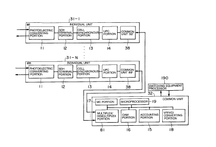
FIG. 3 is a block diagram showing a separate
configuration example of the line interface within the
ATM switching equipment illustrated in FIG. 2. That is,
the line interface 3 is separated into the individual
units and the common unit. Referring to FIG. 3, the
line interface 3 is constructed of a plurality of
0-system individual units 31-1 through 31-N and the
0-system common unit 32, connected to the plurality of
individual units 31, for batch-processing the cells
processed in the plurality of individual units 31,
respectively.
The individual units 31-1 to 31-N convert data
transmitted from the subscriber's terminals 1 on the
cell unit and transfer the data to the common unit 32.
214483'
- 38 -
Each of the individual units 31-1 to 31-N is constructed
of a photoelectric converting portion 11, an SDH
terminal portion 12 connected to the photoelectric
converting portion 11, a cell synchronous portion 13
connected to the SDH terminal portion 12, a UPC portion
14 connected to the cell synchronous portion 13 and a
common interface (INF) 38 connected to the UPC portion
14 and the common unit 32 as well.
The photoelectric converting portion 11 converts
optical signals from the subscriber's line 53 each
composed of a optical cable into electric signals or
inversely converts the electric signals into optical
signals. The SDH terminal portion 12 terminates the SDH
format sent from the subscriber's terminal 1.
The cell synchronous portion 13 performs cell error
control on the basis of header error control data
written to a cell header and effects a cell synchronous
detection.
The UPC portion 14 manages a band to be used by the
subscriber by monitoring traffic density. The common
INF 38 transfers the cell data to the common unit 32.
The common unit 32 transfers the cells from the
plurality of individual units 31-1 through 31-N to the
switch 4 as shown in Fig. 2. The common unit 32
includes a multiplex/demultiplex portion 81, an OAM
portion 16, an MC portion 17, an accounting portion 15,
a VPI/VCI converting portion 18 and a microprocessor 19.
2144~3~
- 39 -
The multiplex/demultiplex portion 81 multiplexes
the cells sent from the individual units 31-1 to 31-N or
demultiplexes the cells with respect to the individual
units 31.
The accounting portion 15 collects pieces of
accounting data by counting the number of the cells
inputted. The OAM portion 16 manages an OAM cell (alarm
cell). The MC portion 17 monitors a cell quality by
measuring a cell error characteristic, a cell loss
characteristic and a cell delay characteristic by use of
MC cells.
The VPI/VCI converting portion 18 reads a VPI/VCI
from the cells inputted, converts this VPI/VCI into a
new output destination VPI/VCI corresponding to the
former VPI/VCI.
The microprocessor 19 controls the
multiplex/demultiplex portion 81, the accounting portion
15, the OAM portion 16, the MC portion 17 and the
VPI/VCI converting portion 18.
A switching equipment processor 190 is connected to
the microprocessor 19. The switching equipment
processor 190 notifies the individual units 31-1 through
31-N of a control command for controlling the individual
units 31-1 through 31-N and a trouble monitoring command
for monitoring troubles in the individual units 31-1
through 31-N.
In the discussion given above, the cell is
2144837
- 40 -
transferred from the subscriber's terminal 1 via the
line interface 3 to the switch 4. In the reverse order
to this, the cell may be transferred from the switch 4
via the line interface 3 to the subscriber's terminal 1.
According to such a construction, the OAM portion
16. the MC portion 17 and the VPI/VCI portion 18
incorporated into the common unit 32 are employed in
common for the individual units 31-1 through 31-N, and,
therefore, down-sizing of the line interface 3 is
attained.
Further, the operation of the switching equipment
processor 190 is carried out in the procedures which
follow. To start with, the switching equipment
processor 190 transmits the control command and the
trouble monitoring command to the microprocessor 19,
which receives these commands. The microprocessor 19
analyzes which individual unit is to receive the command
and transmits the control command or the trouble
monitoring command to the corresponding individual unit.
Next, when the individual unit receiving the
command transmits a reply (status) to the command to the
microprocessor 19, the microprocessor 19 sends this
replay back to the switching equipment processor 190.
That is, the switching equipment processor 190 is
capable of controlling the individual units 31-1 through
31-N through the microprocessor 19.
FIG. 4 is a block diagram illustrating a separate
' ,,..,
21~4~3~
- 41 -
configuration example 2 of the line interface. In
contrast with the separate configuration example 1 shown
in FIG. 3, the separate configuration example 2 provides
the common unit with the UPC portion 14 but removes the
UPC portion 14 from each of the individual units 31-1
through 31-N.
More specifically, each of the individual units
31A-1 through 31A-N is constructed of the photoelectric
converting portion 11, the SDH terminal portion 12
connected to the photoelectric converting portion 11, a
cell synchronous portion 13a connected to the SDH
terminal portion 12 and a common INF 38 connected to
cell synchronous portion 13a. The common unit 32A is
constructed of the multiplex/demultiplex portion 81, the
accounting portion 15, the UPC portion 14, the OAM
portion 16, the MC portion 17, the VPI/VCI converting
portion 18 and the microprocessor 19 for controlling
these portions. The switching system processor 190 is
connected to the common unit 32A.
The cell in each of the individual units 31A-1 to
31A-N consists of a data cell in which the data is
decomposed to a fixed length, a clock pulse
synchronizing with the data cell, a cell enable signal
indicating whether the data cell is valid or not and a
cell frame signal having a bit indicating a heading of
the data cell.
Further, three signal lines 54 are connected
.. , 214483'
- 42 -
between each of the individual units 31A-1 through 31A-N
and the common unit 32A per the individual unit.
Referring to FIG. 4, the single signal line 54 is shown
for simplicity. As illustrated in FIG. 5B, the data
cell is transferred in the form of a serial signal
(serial data) to the common unit via one of these three
signal lines 54.
The remaining two signal lines serve to transfer a
cell frame signal FRM defined as an identifier
indicating a heading of the cell and a clock pulse CLK
synchronizing with the data cell to the common unit 32A.
The cell frame signal FRM outputs "H" by only one bit in
synchronism with the cell heading but keeps an "L"
status during a period other than the above-mentioned.
The cell synchronous portion 13a performs the
processing shown in the separate configuration example 1
and at the same time writes, to within the header, the
cell enable signal ENB defined as an identifier
indicating whether the cell is valid or not. The cell
enable signal ENB, if the cell is valid, outputs "H" and
"L" if the cell is invalid.
Note that other constructions are the same as those
in the separate configuration example 1, and hence their
details will be omitted.
According to this construction, there is attained
more down-sizing of the individual units 31A-1 through
31A-N than in the separate configuration example 1 since
',
,. . 214~~3~
- 43 -
the UPC portions 14 have been removed from the
individual units.
Further, the data cell is transferred via the
single signal line 54, and, therefore, the number of the
signal lines is less by fifteen than the number of the
signal lines in the conventional parallel transfer shown
in FIG. 5A, i.e., in FIG. 52A. Further, as the cell
enable signal is written to the header, the signal lines
54 for the cell enable signals are eliminated.
That is, the data cell, the clock pulse and the
cell frame signal are transferred through the three
signal lines 54, and hence the number of the signals
lines a.s less by sixteen than the nineteen signal lines
54 employed in the conventional parallel transfer.
Accordingly, when a plurality of lines are
accommodated, the number of the signal lines is greatly
reduced having a large effect on the size of the line.
Note that the cell enable signal written to the
header works to distinguish whether the data cell is
valid or invalid in the example given above. For
instance, as illustrated in FIG. 6, whether the data
cell is valid or not may be distinguished depending on
the existence or non-existence of the frame signal
indicating the heading of the data cell. In this case,
the frame signal consists of "H" indicating the
validness of the frame or "L" indicating the invalidness
of the frame.
2144837
- 44 -
As mentioned previously, the cell enable signal
(ENB) outputs "H" (high) status until the next frame
pulse (FRM) but keeps "L" (low) status during other
periods. It is possible to multiplex the enable signal
into the frame signal. In this way the cell top can be
discriminated by the resulting pulse outputting "H" for
two bits when the cell is valid and outputting "H" for
only one bit when the cell is invalid. Since the frame
pulse would now be outputted periodically, it is
possible to discriminate the taking out and putting in
of the package based on the frame pulse.
Furthermore, if line speed increases, the data cell
can not be serially transferred via the single signal
line. In this case, a plurality of signal lines are
prepared corresponding to the line speed, and the data
cells may be transferred in parallel through the
respective signal lines. For instance, if the line
speed is 156 Mbps, the data cell is serially transferred
via the single signal line. 4Jhen line speed increases
up to 600 Mbps, as illustrated in FIG. 7, the data cells
are transferred in parallel via four signal lines.
FIG. 8 is a block diagram illustrating a separate
configuration example 3 of the line interface. In the
separate configuration example 3, each of the individual
units 31B-1 through 31B-N is constructed of the
photoelectric converting portion 11, the SDH terminal
portion 12 connected to the photoelectric converting
214483'
- 45 -
portion 11, a cell synchronous portion 13b connected to
the SDH terminal portion 12, a line number portion 39
for generating line numbers of the subscriber's line 53
connected to the self individual units and the common
INF 38 connected to cell synchronous portion 13b.
The common unit 32B is constructed of the
multiplex/demultiplex portion 81, the accounting portion
15, the UPC portion 14, the OAM portion 16, the MC
portion 17, the VPI/VCI converting portion 18 and the
microprocessor 19 for controlling these portions. The
switching system processor 190 is connected to the
common unit 32B.
The line number portion 39 is connected to the cell
synchronous portion 13b which, in turn, adds a line
number 390 generated by the line number portion 39 to
the cell header in the form of an identification flag.
The common unit 32B performs the cell processing
per line on the basis of the line number 390 added to
the cell header within the cell sent from each of the
individual units 31B-1 through 31B-N.
According to such a construction, the line number
portion 39 provided in each individual unit adds the
line number 390 to the cell header and transfers it to
the common unit 32B. The common unit 32B is capable of,
while referring to the respective line numbers,
distinguishing which line to transfer each of the data
cells inputted.
~~w .
_214~~3~'
- 46 -
FIG. 9 is a block diagram illustrating a separate
configuration example 4 of the line interface. In the
separate configuration example 4, each of the individual
units 31C-1 through 31C-N is constructed of the
photoelectric converting portion 11, the SDH terminal
portion 12, the cell synchronous portion 13a, the line
number portion 39 for generating line numbers of the
subscriber's line 53 connected to the self individual
units and the common INF 38.
The common unit 32C is constructed of the
multiplex/demultiplex portion 81, the accounting portion
15, the UPC portion 14, the OAM portion 16, the MC
portion 17, the VPI/VCI converting portion 18 and the
microprocessor 19 for controlling these portions. The
switching system processor 190 is connected to the
common unit 32C.
The line number portion 39 provided in each
individual unit is connected via a signal line 56 to the
multiplex/demultiplex portion 81. The common unit 32C
effects the cell processing per line on the basis of the
line numbers 390 sent from the line number portions 39
provided in the individual units 31C-1 through 31C-N.
That is, the line number 390 generated in the line
number portion 39 is transferred as an identification
flag directly to the common unit 32C, and hence the same
effect as the above-discussed separate configuration
example 3 is obtained.
a _2144837
- 47 -
The embodiment discussed above has presented the
example where the line interface in the ATM switching
equipment is separated into a common unit and individual
units. Given next is an explanation of an example where
the line interfaces are provided corresponding to the
subscriber's line.
FIG. 10 illustrates another configuration example
of the line interface. One subscriber's terminal 1 is
connected via the subscriber's line 53 to this line
interface 3A. The switch 4 is connected to an output of
the line interface 3A. That is, this line interface 3A
is provided corresponding to one subscriber's
terminal 1.
Herein, the line interface 3A is characterized by a
separation into a processing unit for processing the
cells in real time and a processing unit for processing
the cells while permitting a time delay.
The line interface 3A includes the photoelectric
converting portion 11, the SDH terminal portion 12, the
cell synchronous portion 13, the MC portion 17 connected
to the cell synchronous portion 13, a block portion 160
connected to the MC portion 17 and the microprocessor
19. The microprocessor 19 controls the MC portion 17
and the block portion 160 as well.
The MC portion 17 monitors the cell quality by
measuring the cell error characteristic, the cell loss
characteristic and the cell delay characteristic by use
214483'
- 48 -
of the MC cells. For this purpose, the MC portion 17 is
required to make an extraction timing and an insertion
timing of the MC cell coincident with each other. That
is, the MC portion 17 processes the MC cells in real
time.
The block portion 160 provides blocked processes
permissible even when there is a deviation between the
extraction and insertion timings of an item of header
data and an OAM cell.
The block portion 160 blocks, e.g., the UPC portion
14, the accounting portion 15, the OAM portion 16 and a
header conversion portion 18.
FIG. 11 illustrates a specific configuration of the
block portion. The block portion 160 includes a cell
extracting portion 162, a cell inserting portion 164
connected to the cell extracting portion 162 and a cell
processing portion 166 connected to the cell extracting
portion 162 and the cell inserting portion 164. The
cell extracting portion 162 extracts the header data and
a preset item of specific OAM cell data from the cells
inputted and outputs these items of data to the cell
processing portion 166.
The cell processing portion 166 is constructed of
the UPC portion 14, the accounting portion 15, the
header conversion portion 18 and the OAM portion 16.
The cell processing portion 166 is constructed so that
each element of the cell processing portion 166 uses the
. 214837
- 49 -
cell extracting portion 162 and the cell inserting
portion 164 in common.
The UPC portion 14 inputs the header data extracted
by the cell extracting portion 162 and determines
whether or not an inflow of the cells is permitted on
the basis of this item of header data. The UPC portion
14, if the cell inflow should not be permitted,
indicates to the cell inserting portion 164 to dispose
of the cells.
The accounting portion 15 inputs the header data
extracted by the cell extracting portion 162 and counts
the number of cells on the basis of this item of header
data, thereby collecting pieces of accounting data.
The header conversion portion 18 inputs the header
data extracted by the cell extracting portion 162,
converts this item of header data into a new item of
header data and output the thus converted header data to
the cell inserting portion 164.
The OAM portion 16 inputs the OAM cell data
extracted by the cell extracting portion 162 and
performs both cell receive processing and a creation of
the OAM cells with respect to this item of OAM cell
data.
The cell inserting portion 164 disposes of the
cells in conformity with the cell loss indication sent
from the UPC portion 14 within the cell processing
portion 166. The cell inserting portion 164 re-adds the
_ 21448~~
- 50 -
new item of header data to the cell header in accordance
with the new header data sent from the header conversion
portion 18 within the cell processing portion 166. The
cell inserting portion 164 inserts the OAM cell in
accordance with the OAM cell data sent from the OAM
portion 16 within the cell processing portion 166.
The operations given above are those on the
upstream side from the subscriber's terminal 1 to the
switch 4.
Note that only the accounting portion 15 and the
OAM portion 16 operate on the downstream side from the
switch 4 to the subscriber's terminal 1 as shown in FIG.
12. In this case, the UPC portion 14 and the header
conversion portion 18 do not operate.
In accordance with the embodiment illustrated in
FIG. 10, the line interface 3A is separated into the MC
portion 17 for demanding a coincidence of the extraction
and insertion timings of the MC cells and the block
portion 160 in which there is permitted some deviation
between the extraction timing and the insertion timing
of the header data and the OAM cell data. Then, the UPC
portion 14, the accounting portion 15, the header
conversion portion 18 and the OAM portion 16 that are
provided in the block portion 160 employ the single cell
extracting portion 162 and the single cell inserting
portion 164 in common, thereby attaining the desired
down-sizing of the line interface 3A.
_214487
- 51 -
FIG. 13 illustrates a separate configuration
example 5 of the line interface. In the separate
configuration example 5, the cell processing by the
block portion shown in FIG. 10 is applied to each of the
individual units and the common unit.
Each of the plurality of individual units 31D-1
through 31D-N is constructed of the photoelectric
converting portion 11, the SDH terminal portion 12, the
cell synchronous portion 13, a cell processing portion
166a, the common INF 38, the cell extracting portion 162
connected to the cell processing portion 166a and the
cell inserting portion 164 connected to the cell
processing portion 166a.
The cell processing portion 166a is constructed of
the UPC portion 14 and the accounting portion 15. The
UPC portion 14 and the accounting portion 15 use the
cell extracting portion 162 and the cell inserting
portion 164 in common.
The common unit 32D includes the
multiplex/demultiplex portion 81, the cell processing
portion 166b, the header conversion portion 18, the cell
extracting portion 162 connected to the cell processing
portion 166b and the cell inserting portion 164
connected to the cell processing portion 166b. The cell
processing portion 166b is composed of the OAM portion
16 and the header conversion portion 18. The OAM
portion 16 and the header conversion portion 18 use the
. ..T. . . _
214483
- 52 -
cell extracting portion 162 and the cell inserting
portion 164 in common.
Such a construction attains more down-sizing of the
individual units and the common unit than in the
construction to provide the cell extracting portion 162
and the cell inserting portion 164 for every unit.
FIG. 14 is a block diagram showing a separate
configuration example 6 of the line interface. The ATM
switching equipment 10 incorporates one or a plurality
of line interfaces 3. Each line interface 3 is provided
corresponding to a plurality of subscriber's terminals
1.
The line interface 3 shown in FIG. 14 includes a
plurality of individual units 31-1 through 31-N,
provided corresponding to the plurality of subscriber's
terminals 1, for individually processing the cells and
one common unit 32, connected to the plurality of
individual units 31, for batch-processing the cells
processed in the plurality of individual units 31,
respectively.
Each of the individual units 31-1 to 31-N is
constructed of the photoelectric converting portion 11,
the SDH terminal portion 12, the cell synchronous
portion 13, the UPC portion 14, the accounting portion
15 and the common interface INF 38 connected to the
common unit 32.
The common unit 32 is constructed of the
-,-.,.r.
_ 2144~3~
- 53 -
multiplex/demultiplex portion 81 for multiplexing or
demultiplexing the cells, the OAM portion 16, the MC
portion 17 and the VPI/VCI converting portion 18. Note
that the same elements as those shown in FIG. 3 are
marked with the like symbols, and their explanations
will be omitted. The multiplex/demultiplex portion 81,
when effecting the multiplexing, transfers the cell data
from the plurality of lines in the form of serial data.
According to such construction, the OAM portion 16,
the VPI/VCI converting portion 18 which are provided in
the common unit 32 are employed in common to each
individual unit, and, therefore, the configuration of
the line interface 3 can be simplified.
Next, there will be explained an example of the
line interface for directly accommodating the
subscriber's line. That is, one line interface is
provided corresponding to one subscriber's line.
FIG. 15 is a diagram illustrating a construction of
the ATM switching equipment including the line interface
for directly accommodating the subscriber's line in
accordance with an embodiment 2. As illustrated in FIG.
15, an ATM switching equipment 10-1 comprises a line
interface 3 (3-1, 3-2) constituting a subscriber line
interface, a switch 4 (4a, 4b) for switching the cell
and a transit line interface 30 (30a, 30b).
The line interface 3 is conceived as an interface
for converting signals sent with a synchronous digital
_ X14 ~83~
- 54 -
hierarchy (SDH) from the subscriber's terminals 1 in an
ATM format and transmitting the signals to the switch 4.
The switch 4 switches an internal signal path to
transmit a generated cell based on the ATM format to one
of trunk lines.
The subscriber's terminal 1 is connected directly
to a line interface 3-1 via the subscriber's line 53
composed of an optical cable having optical fibers. The
subscriber's terminal 1 is connected via the
subscriber's line 53 and a private branch exchange (PBX)
2 to a line interface 3-2.
That is, in this embodiment the single line
interface 3 directly accommodates one subscriber's
terminal 1. Herein, the optical fiber contains a core
and a clad, whereby a transmission loss is small.
In the configuration example 1 shown in FIG. 15,
since the conventional transmission system 57
illustrated in FIG. 53 is not employed, the
configuration can be simplified. Further, the line
interface 3 is provided corresponding to the
subscriber's line 53, and, hence, even if a fault occurs
in a certain line interface, only the subscriber's line
corresponding thereto is blocked. Accordingly, this
results in an arrangement in which the line is usable
without exerting any influence on other subscribers.
Note that the line interface in this embodiment may
be separated into the above individual units and the
_ 2I4483~
- 55 -
common unit.
FIG. 16 is a diagram illustrating a construction of
the ATM switching system including the line interface
for directly accommodating the subscriber's line in
accordance with an embodiment 3. In the configuration
example 2 shown in FIG. 16, the line interface in the
ATM switching system is based on a dual construction.
More specifically, an ATM switching system 10-2
includes line interfaces 3a-1, 3a-2 as a 0-system
(active system). The ATM switching equipment 10-2 also
includes line interfaces 3b-1, 3b-2 as a 1-system
(standby system).
Further, the ATM switching equipment 10-2 is
equipped with a switching unit 40-1 for switching the
0-system line interface 3a-1, the 1-system line
interface 3b-1 and a switching unit 40-2 for switching
the 0-system line interface 3a-2 and the 1-system line
interface 3b-2. Note that the switch 4 (4a, 4b), the
transit line interface 30 (30a, 30b) are constructed the
same as those in the configuration example 1 illustrated
in FIG. 15.
According to such a construction, for instance, if
a fault occurs in the 0-system line interface 3a-1, the
switching unit 40-1 performs switching from the 0-system
line interface 3a-1 to the 1-system line interface 3b-1.
A disconnection of the line can be thereby prevented,
and this leads to an improvement in terms of reliability
_.
X14 483 ~
- 56 -
of the equipment.
Note that the line interface in this configuration
example 2 may be separated into the above individual
units and the common unit.
FIG. 17 is a diagram illustrating a construction of
the ATM switching system including the line interface
for directly accommodating the subscriber's line in
accordance with an embodiment 4. In the configuration
example 3 shown in FIG. 17, N-sets of the 0-system line
interfaces 3-1 through 3-N use one set of 1-system line
interface 3-(N+1).
That is, an ATM switching system 10-3 includes
0-system N-sets of the line interfaces 3-1 to 3-N,
N-sets of the switching units 41-1 to 41-N corresponding
thereto and a switching unit 42 connected to the
switching units 41-1 through 41-N and the 1-system line
interface 3-(N+1). The ATM switching system 10-3 also
includes a switching unit 43 connected to the 1-system
line interface 3-(N+1) and N-sets of the 0-system line
interfaces 3-1 through 3-N.
Note that switching units 41-1 through 41-N are
provided corresponding to N-sets of subscriber's
terminals 1-1 through 1-N. Other constructions are the
same as those in the configuration example 1.
According to such a construction, if a fault occurs
in, e.g., the line interface 3-1 among N-sets of the
0-system line interfaces 3-1 through 3-N, the switching
-_
_ 2144837
- 57 -
unit 41-1 effects switching from terminal a to terminal
b. Then, the switching unit 41-1 is connected via the
switching unit 42 to the 1-system line interface
3-(N+1).
Namely, the switching unit 41-1 effects switching
from the 0-system line interface 3-1 undergoing the
fault to the 1-system line interface 3-(N+1). The line
disconnection can be thereby prevented, and this brings
about the improvement in reliability of the equipment.
Further, a plurality of 1-system line interfaces
may be provided. In this case, if a fault occurs in the
0-system line interface, the fault line interface may be
switched over to one of the plurality of 1-system line
interfaces.
Incidentally, if all of the plurality of 1-system
line interfaces are employed, the switch-over from the
0-system to the 1-system can not be carried out, and
therefore the relevant line is blocked.
Note that the line interface in this configuration
example 3 may be separated into the above individual
units and the common unit.
FIG. 18 is a block diagram illustrating a
configuration in an example 1 of the line interface
shown in FIGS. 15 to 17. The line interface 3
illustrated in FIG. 18 is down sized from the
conventional line interface.
Referring to FIG. 18, the photoelectric converting
_ 2144837
- 58 -
portion (OE/EO converting portion) 11 converts an
optical signal from the subscriber's line 53 composed of
an optical cable into an electric signal or inversely
converts the electric signal into the optical signal.
The cell synchronous portion 13 is connected to this
photoelectric converting portion 11.
The cell synchronous portion 13 performs the cell
error control on the basis of the header error control
data written to the cell header and effects the cell
synchronous detection. This cell consists of a 5-byte
header (cell header) and a 48-byte data field.
FIG. 19 shows a cell format in the ATM. A cell 200
shown in FIG. 19 consists of a header 201 and a data
field 202.
The header 201 comprises 4-bit flow control data
(GFC; Generic Flow Control), an 8-bit VPI, a 12-bit VCI,
3-bit cell format data (PTI; Payload Type Identifier),
cell loss priority data (CLP; Cell Loss Priority) and
8-bit control data (HEC; Header Error Control) of the
header 201.
The ATM switching equipment operates to allocate
pieces of routing data defined as call identification
labels when setting a call and to release the routing
data when releasing the call. An intrinsic value is
allocated to the routing data for every node-to-node
link. It is required that the routing data be
transformed when passing though every node each time.
_ 2.~~~~3~'
- 59 -
For this purpose, the header converting portion 18 is
provided.
The OAM portion 16 is connected via a fixed
accounting portion 151 to the cell synchronous portion
13. The OAM portion 16 manages an OAM CELL (alarm
cell). The MC portion 17 is connected to this OAM
portion 16.
The MC portion 17 monitors the cell quality by
measuring the cell error characteristic, the cell loss
characteristic and the cell delay characteristic by use
of the MC cells.
A VPI converting portion 18a reads a VPI inputted,
fetches a new output destination VPI corresponding
thereto from a VPI conversion table 180a and rewrites
the header.
The VPI conversion table 180a is composed of a
memory accessible from the VPI converting portion 18a.
The VPI conversion table 180a, as illustrated in FIG.
20, allocates tag data (TAG) and an output destination
VPI (Network Node Interface; NNI) to the VPI (User Node
Interface; UNI) inputted. An output destination path is
determined per cell by this output destination VPI.
The microprocessor 19 controls the fixed accounting
portion 151, the OAM portion 16, the MC portion 17 and
the VPI converting portion 18a.
(a) According to the thus constructed line
interface, to start with, the VPI converting portion 18a
_ 211183'
- 60 -
converts only the VPI by referring to the conversion
table 180a shown in FIG. 20 but does not effect a VCI
conversion. It is therefore possible to reduce the
memory capacity of the conversion table by the number of
bits of the VCI in the VCI conversion.
In this case, even when performing no VCI
conversion, it is feasible to actualize a user virtual
path (UVP) service in which the subscriber uses a
virtual path (VP) as if it is a dedicated line.
(b) Next, the UPC portion 14 is provided in the
conventional line interface but eliminated in the line
interface 3 illustrated in FIG. 18. Instead, the line
interface 3 is equipped with an overall band portion 141
for notifying the microprocessor 19 not to exceed a
usage quantity of the band.
This overall band portion 141 is capable of
actualizing a service in which overall line bands given
are freely used.
Further, the overall band portion 141 is not
required to monitor a flow rate of the cells as in the
case of the UPC portion 14 by its being connected to the
cell synchronous portion 13 and can therefore have a
simple construction than the UPC portion 14.
(c) Also, in the line interface 3 shown in FIG. 18,
the configuration of the accounting portion 15 is made
simpler than in the conventional line interface.
The conventional accounting portion 15 collects
,w.,. .
,. , _2144837
- 61 -
pieces of accounting data by counting the number of
cells. The fixed accounting portion 151 of Fig. 18 is
connected to the cell synchronous portion 13 and
notifies the microprocessor 19 of being a subscriber for
a fixed charge. That is, since the cells are not
counted, the configuration can be simplified, and, at
the same time, it is possible to actualize the service
of setting the fixed charge without depending on the
amount of line usage.
In this case, if a different line interface is
provided for every service, the efficiency decreases.
For example, there may be employed a service combined
with the above-mentioned, i.e., a dedicated line service
in which the line bands are freely used, and, besides,
the charge is fixed irrespective of the amount of usage.
If use of this dedicated line increases, the hardware
quantity can be further reduced by use of a line
interface dedicated to the service.
(d) Further, the SDH terminal portion 12 is
provided in the conventional line interface but
eliminated in the line interface 3 illustrated in FIG.
18. In the prior art, a physical layer between the
subscriber's terminal 1 of the user and the network is
an SDH format. The SDH terminal portion 12, as
illustrated in FIG. 56, terminates the SDH format. An
SDH frame is thereby mapped on the ATM cell.
Thereafter, the cell mapped by the cell synchronous
_214437
- 62 -
portion is decomposed.
In the example shown in FIG. 18, full-ATMing is
attained by removing the SDH terminal portion 12.
Thus, the down-sizing of the line interface is
attainable by removing some elements within the line
interface 3 shown in FIG. 18 or simplifying the
configuration thereof. Note that any one or more
configurations explained in the above items (a) through
(d) may be combined.
It should be also noted that the line interface 3
in this example may be separated into the above
individual units and the common unit.
FIG. 21 is a block diagram showing the principal
elements in an example 2 of the line interface shown in
FIG. 15. Referring to FIG. 21, there are shown a
VPI/VCI converting portion 18b and VPI/VCI conversion
tables 180, 181 accessible therefrom. Other
configurations are the same as those shown in FIG. 18.
The example 2 is characterized by reducing a
configuration of the VPI/VCI conversion table 181 for
ordinary subscribers.
In the example shown in FIGS. 15 to 17, the line
interface 3 directly accommodates the subscriber line
53. With this arrangement, the subscriber's terminal 1
of the ordinary subscriber or the private branch
exchange (PBX) 2 is connected to the subscriber's line
53, and, therefore, the subscriber's terminal 1 of the
2144837
- 63 -
ordinary subscriber and the PBX 2 are separated from
each other per subscriber's line 53.
The VPI/VCI conversion table 180 is provided for
the subscribers who use the PBX 2, while the VPI/VCI
conversion table 181 is provided for the ordinary
subscribers.
The subscribers who employ the PBX 2 have a greater
possibility of using the virtual path (VP) and the
virtual channel (VC).
Accordingly, the VPI/VCI conversion table 180 shown
in FIG. 21 stores the VPI and the VCI in the UNI as well
as storing the TAG, the VPI and the VCI in the NNI.
Note that the TAG (tag) is used for the in-system
control (switch routing data).
In the UNI, the VPI consists of 8 bits (256 lines),
while the VCI consists of 16 bits (65536 lines). The
numbers of the VPIs and of the VCIs that are actually
employed are determined between the subscribers and the
network.
In contrast with this, there is almost no
possibility in which the ordinary subscribers of the
subscriber's terminals 1 use all the 8-bit VPIs and the
16-bit VCIs. For this reason, as illustrated in FIG.
21, the VPI consists of 3 bits (8 lines), while the VCI
consists of 5 bits (32 lines) in the UNI of the VPI/VCI
conversion table 181.
In this case, the memory capacity needed for the
214 483'
- 64 -
VPI/VCI conversion table 181 can be reduced down to
28/224, i.e., 1/65536 of the memory capacity for the
VPI/VCI conversion table 180. This results in a large
saving.
As described above, the conversion table of Fig. 21
is divided into the table for the ordinary subscribers
and the table for the PBX subscribers. Restricted are
the numbers of the VPIs and of the VCIs of the VPI/VCI
conversion table 181 which could be used for the
ordinary subscribers. Thus, the memory capacity for use
is reduced, thereby making it possible to decrease the
amount of hardware. Note that the line interface may be
separated into the above individual units and the common
unit.
Next, FIG. 22 is a block diagram showing the
principal elements in an example 3 of the line interface
shown in FIG. 15. Referring to FIG. 22, there are shown
a VPI/VCI converting portion 18c, a VPI/VCI conversion
table 182 before being reduced, first and second
conversion tables 183, 184 and a VP switch table 185.
The example 3 is characterized by reducing the
configuration of the VPI/VCI conversion table 182.
At first, the VPI is used for a service
classification, a ground identification of the dedicated
line and a carrier identification. For instance, as
illustrated in FIG. 23, the VPI is employed for eight
types of services such as telephones, FAX, data
2144837
- 65 -
communications and dedicated lines. Shown also are the
numbers of VCIs accessing to the respective VPIs with
respect to a case 1 and a case 2.
Herein, as can be understood from the case 1 shown
in FIG. 23, the number of users per line is limited.
For this reason, when effecting a plurality of accesses
to one VP, a multiplicity of VCs are needed for
identifying each call. On the other hand, as can be
understood from the case 2 shown in FIG. 23, when
performing the access to the plurality of VPs, the
number of VCs required per VP is small.
Then, the VPI/VCI of the VPI/VCI conversion table
182 is reduced by use of the first and second conversion
tables 183, 184 shown in FIG. 22. In the UNI of the
VPI/VCI conversion table 182, the VPI is set to 3 bits,
while the VCI is set to 5 bits. In the NNI, the VPI is
set to 12 bits, while the VCI is set to 16 bits. The
TAG is set to 12 bits.
In the first conversion table 183, the usable VPI
is set to 3 bits; the VCI is set to 5 bits; and an
internal identifier indicating the number of all the
simultaneously usable VCIs is set to 6 bits.
In this case, there are provided the internal
identifiers, the number of which corresponds to the
number of all the VCIs. Further, an active status of
the internal identifier is managed so as not to employ
the same internal identifier in a different VPI/VCI.
2144837
- 66 -
In the second header conversion table 184, the
internal identifier is set to 6 bits; the VPI in the NNI
is set to 12 bits; and the VCI is set to 16 bits. The
TAG is set to 12 bits.
According to such conversion tables 183, 184, the
VPI/VCI converting portion 18c temporarily converts the
VPI/VCI of the transmitted cell into an internal
identifier by use of the first conversion table 183.
Further, the VPI/VCI converting portion 18c converts the
converted internal identifier into a header for
transmission by use of the second conversion table 184.
For example, the conversion table 183 can employ 8
pieces (3 bits) of VPIs and 32 pieces (5 bits) of VCIs.
If the plurality of VPs are used simultaneously, 64 (6
bits) combinations are available.
In this instance, a reduction rate of the first
conversion table 183 with respect to the VPI/VCI
conversion table 182 is in the order of 1/7 as can be
seen from the following formula:
(1) 28 x 6 / (28 x 40)
where the numeral 40 indicates a sum of the VCIs used.
Further, a reduction rate of the third conversion
table 184 with respect to the VPI/VCI conversion table
182 is in the order of 1/4 as can be seen from the
following formula:
(2) 26 x 40 / (28 x 40)
Thus, there is restricted the number of all the
2144837
- 67 -
VCIs using the plurality of VPs at the same time with
the 6-bit internal identifier by use of the first and
second conversion tables 183, 184. The memory capacity
can be thereby decreased.
Also, a VP switch table 185 shown in FIG. 22 stores
a 3-bit VPI, a 1-bit UVP indicating whether or not only
a UVP service is offered without effecting a VC
conversion and a 6-bit internal identifier.
When using the VP switch table 185, no VCI
conversion is carried out. Hence, only one internal
identifier is employed in one VP. In this case, a
reduction rate of the VP switch table 185 with respect
to the VPI/VCI conversion table 182 is approximately
1/200 as can be seen from the following formula:
(3) 23 x 7 / (28 x 40)
Thus, the memory capacity can be remarkably
reduced. Note that the line interface 3 in this example
may be separated into the above individual units and the
common unit.
(Example 1 of Switching System of Individual Unit)
FIG. 24 is a block diagram showing an example 1 of
a system switching system if a fault occurs in the
individual unit.
A system switching system illustrated in FIG. 24 is
a more concrete version of the configurations shown in
FIG. 2 and 3. The line interface includes N-sets of
individual units 31-1 through 31-N of the active system
. 214483'
- 68 -
i.e., the 0-system, one individual unit 34 of the
standby system, viz., the 1-system and 0- and 1-system
common units 32a, 32b corresponding thereto.
Corresponding 0- and 1-system switches 4a, 4b are
connected to these common units 32a, 32b irrespectively.
Each of N-sets of the 0-system individual units
31-1 to 31-N outputs, if the fault occurs in the
individual unit itself, a fault line identifier 36 to
the common unit 32 and an optical selector 60 which will
be discussed later. The optical selector 60 connects
N-lines of lines on the input side to N-sets of the
0-system individual units 31-1 through 31-N and, upon
receiving the fault line identifier 36 from the fault
individual unit, switches over the fault individual unit
to the 1-system individual unit 34. An optical decoder
70 has its input side connected to N-sets of the
0-system individual units 31-1 through 31-N and the
1-system individual unit 34 and also its output side
connected to N-lines of the lines.
According to such a construction, to start with, if
a certain 0-system individual unit, e.g., the individual
unit 31-1 breaks down, the fault line identifier (termed
also a fault flag) 36 is set from the individual unit
31-1 concerned. Then, the fault line identifier 36 is
sent to the common unit 32 and the optical selector 60.
The optical selector 60 sets the fault line identifier
36 as an optical selector switching signal and switches
. _ 2144837
- 69 -
over the fault individual unit 31-1 to the standby
system individual unit 34.
On the other hand, the fault line identifier 36
sent to the common unit 32 turns out a select signal
when the multiplex/demultiplex portion 81 of the common
unit 32 selects N-sets of the individual units from
(N+1) sets of the individual units. The
multiplex/demultiplex portion 81, after removing the
0-system fault individual unit 31-1 out of N-sets of the
individual units, selects the 1-system individual unit
34 and performs multiplexing of N . 1.
The discussion given above deals with the
operations on the upstream side (from the subscriber to
the switch). Note that the downstream side is switched
over simultaneously when switching over the upstream
side. The optical decoder 70 effects switching to the
1-system individual unit 34 to transmit the data from
the downstream side (from the switch to the subscriber),
i.e., from a data transmission side to the fault side.
Note that only one 1-system individual unit 34 is
provided according to the above construction, however,
there may be provided a plurality of the individual
units 34 of, e.g., the 1-system.
FIG. 25 is a diagram illustrating details of the
optical selector 60 for performing the system switching
shown in FIG. 24. Referring to FIG. 25, the optical
selector 60 is constructed of photo couplers 61-1
w _ 2144837
- ~0 -
through 61-N provided corresponding to N-lines of the
subscriber's line 53 and an optical switch 62 connected
to the photo couplers 61-1 through 61-N. The respective
photo couplers 61-1 through 61-N are connected via the
optical fibers 53 to the corresponding 0-system
individual units 31-1 through 31-N.
The optical switch 62, upon receiving the fault
line identifier 36 from one of the 0-system individual
units 31-1 through 31-N, connects the photo coupler
corresponding to the 0-system fault individual unit to
the 1-system individual unit 34 in order to switch over
the 0-system fault individual unit to the 1-system
individual unit 34.
According to this construction, at first, the
optical signal from the optical fiber 53 serving as the
subscriber line is inputted to the optical selector 60
packaged in the line interface.
The optical signals are transmitted to the 0-system
individual units 31-1 through 31-N from the photo
couplers 61-1 through 61-N within the optical selector
60. Herein, if an abnormality is caused in one of the
0-system individual units, the fault subscriber
accommodated in the optical switch 62 is connected to
the 1-system individual unit 34, wherein the fault line
identifier 36 sent from the fault individual unit serves
as a switching signal of the optical switch 62.
Subsequently, a multiplex portion 81a multiplexes
214483
- 71 -
N-pieces of cells of the 1-system individual unit 34 and
the 0-system individual unit.
That is, on the upstream side from the subscriber
to the switch 4, the optical switch 62 performs
switching by use of the fault line identifier 36 sent
from the 0-system fault individual unit, and, therefore,
a restoration can be quickly made. Also, since the
photo couplers 61-1 through 61-N are accommodated in the
optical selector 60, no influence is exerted on the
optical switch 62 even when insert-removing the fault
individual unit.
FIG. 26 is a block diagram illustrating details of
the optical decoder for effecting the system switching
shown in FIG. 24. Referring to FIG. 26, the optical
decoder 70 is constructed of the photo couplers 61-1
through 61-N provided corresponding to N-lines of the
subscriber's line 53 and the optical switch 62 connected
to the photo couplers 61-1 through 61-N. The respective
photo couplers 61-1 through 61-N are connected via the
optical fibers 53 to the corresponding individual units.
The optical switch 62, upon receiving the fault line
identifier 36 from the individual unit, connects the
photo coupler corresponding to the fault individual unit
to the 1-system individual unit 34 in order to switch
over the 0-system fault individual unit to the 1-system
individual unit 34.
According to this construction, if an abnormality
2144~3~
- 72 -
occurs in one of the 0-system individual units, the
fault subscriber accommodated in the optical switch 62
is connected to the 1-system individual unit 34, wherein
the fault line identifier 36 sent from the fault
individual unit serves as a switching signal of the
optical switch 62.That is, on the downstream side from
the switch to the subscriber, the optical switch 62
performs switching by use of the fault line identifier,
and, therefore, the restoration can be quickly made.
FIG. 27 is a block diagram showing an example 2 of
the switching system of the individual unit. In the
switching system illustrated in FIG. 27, the
upstream-side optical selector shown in FIG. 24 and the
downstream-side optical decoder are formed into one
united body.
The subscriber's terminals (TE) 1-11 through 1-1N
include E/O portions lla-1 through 11a-N, O/E portions
llb-1 through llb-N and wavelength division multiplex
(WDM) portions 26-1 through 26-N, connected thereto, for
dividing and multiplexing different wavelengths. The
WDM 26-1 through 26-N input two wavelength ~1, ~2 and
allocate pieces of upstream-side and downstream-side
data.
An optical selector 60a includes N-sets of
photocouplers 61-1 through 61-N common to the upstream
and downstream sides and one optical switch 62. The
WDMs 26-1 through 26-N are connected via the optical
21448~~
- 73 -
fibers 53 to the photocouplers 61-1 through 61-N.
Each of the 0-system individual units 31-11 to
31-1N has the WDMs 26-1 to 26-N, the E/O portions lla-1
to lla-N and the O/E portions llb-1 to 11b-N. A
1-system individual unit 34A includes a WDM 26A, an E/O
portion 11A and an O/E portion 11B.
The common unit 32 includes a multiplex portion 81a
and a demultiplex portion 81b. An output of each of the
O/E portions llb-1 through llb-N is connected via the
cell synchronous portion to the multiplex portion 81a.
Respective outputs of the demultiplex portion 81b are
connected via the cell synchronous portion to the E/O
portions lla-1 through lla-N.
According to the thus constructed optical selector
and a peripheral line, on the upstream side, the optical
signals having the wavelength ~.1 that are converted from
the electric signals by the E/O portions lla-1 to lla-N
through lla-N within the subscriber's terminals (TE)
1-11 to 1-1N are transmitted through the optical fibers
53 via the WDMs 26-1 to 26-N and taken in the
photocouplers 61-1 to 61-N. Then, the optical signals
thereof are, after passing through the WDMs 26-1 to 26-N
within each individual unit, converted into the electric
signals by the O/E portions llb-1 to 11b-N and applied
to the multiplex portion 81a. Further, the multiplex
portion 81a multiplexes the electric signals coming from
the individual units.
214483'
- 74 -
While on the downstream side, the electric signals
corresponding to the wavelength ~,2 demultiplexed by the
demultiplex portion 81b are converted into the optical
signals having the wavelength ~,2 by the E/O portions
lla-1 to lla-N within each individual unit. The thus
converted optical signals are taken in the photocouplers
61-1 to 61-N via the WDMs 26-1 to 26-N and the optical
fibers 53. Thereafter, the optical signals having the
wavelength ~,2 are, after passing through the WDMs in the
TE via the optical fibers 53, converted into the
electric signals by the O/E portions llb-1 to llb-N.
Note that if the trouble occurs in one of the
N-sets of the 0-system individual units, the relevant
individual unit is switched over to the 1-system
individual unit 34A.
That is, bidirectional communications via the
single optical fiber 53 are attainable by effecting
communications using the different wavelengths on the
upstream and downstream sides. Further, the equipment
can be constructed on one surface without changing the
size of the optical selector 60a, and the number of the
optical fibers 53 extending between the equipments can
be reduced down to 1/2 of the number in the example
shown in FIG. 25.
FIG. 28 is a block diagram illustrating an example
3 of the switching system of the individual unit. In
the switching system shown in FIG. 28, TEs 1-21 to 1-2N
2144837
- 75 -
and individual units 31-21 to 31-2N have 2 x 2 couplers
27-1 to 27-N and photo isolators 28-1 to 28-N. The
photo isolators 28-1 to 28-N permit a unidirectional
transmission of the signals. The 2 x 2 couplers 27-1 to
27-N are connected to the photo isolators 28-1 to 28-N.
Each of these 2 x 2 couplers 27-1 to 27-N has two input
terminals and two output terminals and permits a
bidirectional transmission of the signals.
Note that the 2 x 2 couplers 27-1 to 27-N and the
photo isolators 28-1 to 28-N have been added, and the
WDMs 26-1 to 26-N shown in FIG. 27 have been eliminated.
Other configurations are the same as those shown in FIG.
27, and their explanations are omitted.
According to such a construction, on the upstream
side, the optical signals having the wavelength ~,1 are
transmitted through the optical fibers 53 via the photo
isolators 28-1 to 28-N and the 2 x 2 couplers 27-1 to
27-N and taken in the photocouplers 61-1 to 61-N. The
optical signals thereof are converted into the electric
signals by the O/E portions through the 2 x 2 couplers
27-1 to 27-N within each individual unit as well as
through the optical fibers.
While on the downstream side, the electric signals
are converted into the optical signals having the
wavelength 7l2 by the E/O portions within each individual
unit and taken in the photocouplers 61-1 to 61-N via the
photo isolators 28-1 to 28-N and the 2 x 2 couplers 27-1
2144837
- 76 -
to 27-N. The optical signals having the wavelength ~.2
are, after passing through the 2 x 2 couplers 27-1 to
27-N within the TEs 1-21 to 1-2N via the optical fibers
53, converted into the electric signals by the O/E
portions thereof.
The same effects as those by the optical selector
as shown in FIG. 27 are obtained even by use of the
photo isolators 28-1 to 28-N and the 2 x 2 couplers 27-1
to 27-N. Further, in this case, any influence exerted
on the signals coming from the opposite direction is
substantially decreased because of using the photo
isolators.
FIGS. 29 and 30 illustrate an example 4 of the
switching system of the individual unit. FIG. 29 is a
block diagram illustrating the switching system of the
individual unit on the upstream side. FIG. 30 is a
block diagram illustrating the switching system of the
individual unit on the downstream side.
The selector 60b shown in FIG. 29 includes the O/E
portions llb-1 to llb-N and an electric switch 63
connected thereto. A decoder 70b illustrated in FIG. 30
also includes the O/E portions llb-1 to llb-N and the
electric switch 63 connected thereto, Further, the O/E
portions llb-1 through llb-N are connected via electric
signal lines 55 to the 0-system individual units 31-1
through 31-N. A 1-system individual unit 34B is
connected to the electric switch 63.
214.483?
Based on such a construction, the optical signals
coming from the TEs 1-21 to 1-2N are converted into
electric signals by the O/E portions llb-1 to llb-N and
transmitted via the electric signal lines 55 to the
individual units. If constructed in this way, the O/E
portions and the E/O portions do not have to be provided
in the individual units 31-1 through 31-N, thereby
making it possible to reduce the physical size thereof.
(Example of Switching System of Common Unit)
Given next is an explanation of one example of the
switching system of the common unit when the line
interface is separated into the individual units and the
common unit. FIG. 31 is a diagram illustrating a
configuration of (N+1) sets of common units for N-lines
of lines. The line interface depicted in FIG. 31 has
(N+1) sets of common units 32-1 to 32-(N+1) for N-lines
of lines.
The line interface includes N x M sets of
individual units 31-1 to 31-NM corresponding to N x M
lines of subscriber's line, (N+1) sets of common units
32-1 to 32-(N+1) connected respectively to the
individual units and a system selection unit 45
connected to (N+1) sets of the common units 32-1 tv
32-(N+1) and a switch (SW) unit.
Any one (N+1) sets of the common units 32-1 to
32-(N+1) is employed if one of N-sets of the common unit
breaks down. That is, one standby common unit for
_ 214483?'
- 78 _
switching if trouble occurs is provided for N-lines of
the lines.
The individual units and the common units are
connected to each other, whereby outputs from N x M sets
of the individual units 31-1 to 31-NM are distributed to
all of (N+1) sets of the common units 32-1 through
32-(N+1).
Each individual unit includes the photoelectric
converting portion 11, the SDH terminal portion 12 and
the cell synchronous portion 13a in, e.g., the separate
configuration example 4 of the line interface shown in
FIG. 9. The functions of these elements have already
been explained, and hence their descriptions are omitted
herein.
Each of the common units 32 (32-1 through 32-(N+1))
is equipped with multiple/demultiplex portion 81 (81-1
through 81-(N+1)), cell processing portions 166 (166-1
to 166-(N+1)) connected to the multiplex/demultiplex
portions 81-1 through 81-(N+1) and fault notifying
portions 37 (37-1 through 37-(N+1)) connected to the
multiplex/demultiplex portions 81-1 through 81-(N+1).
Each of the multiplex/demultiplex portions 81-1 to
81-(N+1) selects M-sets of the individual units and
outputs the cells from these individual units to the
cell processing portions 166. For example, the
multiplex/demultiplex portion 81-1 selects M-sets of the
individual units 31-1 to 31-M, while the
2144837
- 79 -
multiplex/demultiplex portion 81-N selects M-sets of the
individual units 31-(N-1)M+1 to 31-NM.
Each of the cell processing portions 166-1 to
166-(N+1) includes the OAM portion 16, the UPC portion
14, the accounting portion 15, the VPI/VCI converting
portion 18 in, e.g., the separate configuration example
4 of the line interface as depicted in FIG. 9. The
functions of these elements have already been explained,
and hence their descriptions are omitted herein.
Each of the fault notifying portions 37-1 to
37-(N+1), if a fault occurs in the self individual unit,
notifies all other fault notifying portions of a fault
identification number. Also, the fault notifying
portion provided in the standby system common unit, when
receiving the fault identification number, outputs the
switching signal for switching from the fault common
unit to the self common unit to the self
multiplex/demultiplex portion on the basis of the fault
identification number.
The system selection unit 45 includes the selector
46 for outputting the output data of N-lines of the
lines by selecting N-pieces of outputs with respect to
the (N+1) pieces of inputs from (N+1) sets of the common
units.
Next, the operations of the thus constructed line
interface separated into the individual units and the
common unit will be discussed with reference to a
214483?
- 80 -
flowchart of FIG. 32.
At first, each individual unit performs the
processing such as a cell synchronization (step 1001).
Next, each of the multiplex/demultiplex portions 81-1 to
81-(N+1) selects M-sets of the individual units (step
1002). For instance, the multiplex/demultiplex portion
81-1 selects M-sets of the individual units 31-1 to
31-M, while the multiplex/demultiplex portion 81-2
selects M-sets of the individual units 31-(M+1) to
31-2M.
In this manner, each multiplex/demultiplex portion
selects M-sets of the corresponding individual units,
and the multiplex/demultiplex portion 81-N selects
M-sets of the individual units 31-(N-1)M+1 to 31-NM.
Note that the multiplex/demultiplex portion 81-(N+1)
does not select M-sets of the individual units but lets
these units in the standby system.
Next, the cell processing portions 166-1 to 166-N
within each common unit perform processes such as an
accounting process with respect to the cells from the
corresponding multiplex/dernultiplex portions (step
1003 ) .
Further, each of the fault notifying portions 37-1
to 37-(N+1) determines whether or not any trouble occurs
in the self common unit (step 1004). If no troubles
occurs in the self common unit, the selector 46
transmits the cell data from the common units 32-1
. ~.' , ~ _ 2144837
- 81 -
through 32-N to the SW unit (step 1005).
On the other hand, each of the fault notifying
portions 37-1 through 37-(N+1), if the fault is caused
in the self common unit, notifies all other fault
notifying portions of the fault identification number
(step 1006). For example, if the trouble occurs in the
common unit 32-1, the fault notifying portion 37-1
notifies all other fault notifying portions of the fault
identification number.
At this time, the fault notifying portion 37-(N+1)
provided in the standby system common unit, e.g., the
common unit 32-(N+1) receives the fault identification
number and recognizes the fault common unit from this
fault identification number (step 1007).
The fault notifying portion 37-(N+1) outputs the
switching signal for switching from the fault common
unit 32-1 to the self common unit 32-(N+1) to the self
multiplex/demultiplex portion 81-(N+1) on the basis of
the fault identification number (step 1008).
Then, the standby system common unit 32-(N+1)
selects M-sets of the corresponding individual units
31-1 through 31-M (step 1009), and the operation
proceeds to step 1005.
Thus, in the line interface, (N+1) sets of the
common units are provided for N-lines of lines, and the
individual units and the common units are connected to
each other. One of (N+1) sets of the common units is
. _ 2144837
. ......
- 82 -
set for the standby system. Ulith this arrangement, even
if the trouble occurs in the common unit, the standby
system common unit is usable, and, hence, the cell data
of N-lines of the lines can be continuously processed.
Further, the single standby system common unit
described above is not confined to a given common unit,
e.g., the common unit 32-(N+1), but may be one of (N+1)
sets of the common units. For instance, the common unit
32-1 may be employed for the standby system. In this
case, the arrangement may be, for example, such that the
multiplex/demultiplex portion 81-2 selects M-sets of the
individual units 31-1 to 31-M, while the multiplex/
demultiplex portion 81-(N+1) selects M-sets of the
individual units 31-1(N-1)M+1 to 31-NM.
Moreover, FIG. 33 illustrates a configuration in
which the standby system common unit is fixed in one of
(N+1) sets of the common units. Referring to FIG. 33,
M-sets of the individual units 31-1 to 31-M are
connected to the common unit 32-1. Connected also to
the common unit 32-2 are M-sets of the individual units
31-(M+1) through 31-2M. Similarly, M-sets of the
individual units 31-(N-1)M+1 to 31-NM are connected to
the common unit 32-N. Further, N x M sets of the
individual units 31-1 to 31-NM are connected to the
common unit 32-(N+1).
In this case, one common unit 32-(N+1) is employed
as a fixed standby system common unit. As explained
-w ~ 214483'
- 83 -
above, the standby system common unit shown in FIG. 31
is arbitrarily selectable from (N+1) sets of the common
units. This configuration yields the following effects
as compared with the configuration in which the standby
system common unit illustrated in FIG. 33 is fixed in
one of (N+1) sets of the common units.
More specifically, if the standby system common
unit is fixed, and if a certain active system common
unit breaks down, the standby system common unit is
employed as an active system common unit. Then, when
the active system fault common unit is removed, repaired
and again inserted in the same position, an operation is
required to reset the common unit used for the active
system to the standby system common unit.
However, if the standby system common unit is
arbitrarily selectable, the above setting operation is
not required, and, therefore, the operation can be
eliminated.
(Configuration of Common unit for Accommodating A
Plurality of Individual Units Having Interfaces
Different from Each Other)
Next, FIG. 34 illustrates a configuration of the
common unit for accommodating a plurality of individual
units having interfaces different from each other.
Referring to FIG. 34, the line interface includes two
SDH individual unit interfaces (IF) 35-1, 35-4, two
full-ATM individual units 35-2, 35-3 and a common unit
. .~, , 214483
- 84 -
320 to which the above individual unit IFs are
connected.
A port P1 of the SDH individual unit IF 35-1 is
connected to a port P1' of the common unit, whereby the
SDH individual unit IF 35-1 is packaged in the common
unit 320. A port P2 of the full ATM individual unit IF
35-2 is connected to a port P2' of the common unit,
whereby the full ATM individual unit IF 35-2 is packaged
in the common unit 320. This is the same with the SDH
individual unit IF 35-4 and the full ATM individual unit
IF 35-3.
Each of the SDH individual unit IFs 35-1, 35-4 has
the photoelectric converting portion 11, the SDH
terminal portion 12 connected to the photoelectric
converting portion 11, the cell synchronous portion 13
connected to the SDH terminal portion 12 and an ID
portion 350. The elements exclusive of the ID portion
350 have already been explained in the embodiments
discussed above, and their details are omitted.
The ID portion 350 in the SDH individual unit IFs
35-1, 35-4 sends, to the common unit 320, an
identification number (ID = 0) indicating that the IF
itself is an SDH individual unit IF when the IF itself
is packaged in the common unit 320.
Each of the full ATM individual unit IFs 35-2, 35-3
includes the photoelectric converting portion 11 and the
cell synchronous portion 13 connected to the
_2144837
- 85 -
photoelectric converting portion 11. These elements
have already been explained in the embodiments discussed
above, and their explanations will be omitted. That is,
since the cell is transferred in the ATM format from the
subscriber's line, the SDH terminal portion 12 is
removed. This point is the same as the above-mentioned.
The ID portion 350 in the full ATM individual unit
IFs 35-2, 35-3 sends, to the common unit 320, an
identification number (ID = 1) indicating that the IF
itself is the full ATM individual unit IF when the IF
itself is packaged in the common unit 320.
The common unit 320 is equipped with a control
processor 19a and a cell processing portion 166
controlled by the control processor 19a.
The control processor 19a recognizes the
identification numbers ID sent from the SDH individual
unit IFs 35-1, 35-4 and the full ATM individual unit IFs
35-2, 35-3 and, if these identification numbers are 1,
transmits ATM layer alarm data indication signal to the
full ATM individual unit IFs 35-2, 35-3.
The control processor 19a, if the identification
number is 0, transmits SDH physical layer alarm data
indication signals to the SDH individual unit IFs 35-1,
35-4.
The cell processing portion 166 includes, although
not illustrated, the OAM portion 16, the UPC portion 14,
the accounting portion 15 and the VPI/VCI converting
_... .
_2144837
- 86 -
portion 18. The functions of these elements have
already been explained, and their descriptions are
omitted herein.
Next, the operation of the thus constructed line
interface will be described with reference to FIG. 35.
At the beginning, the control processor 19a determines
whether or not the SDH individual IF or the full ATM
individual unit IF is packaged in the common unit 320
(step 2001).
Herein, for instance, when the full ATM individual
unit IF 35-2 is packaged in the common unit 320 through
the port P2, ID portion 350 sends the identification
number ID = 1 to the control processor 19a.
Thereupon, the control processor 19a transmits the
ATM layer alarm data indication signal to the full ATM
individual unit IF 35-2.
The full ATM individual unit IF 35-2 transmits an
item of ATM layer alarm data about a data error or the
like to the control processor 19a on the basis of the
above indication signal. That is, ATM layer alarm
processing is executed (step 2003).
On the other hand, for example, when the SDH
individual unit IF 35-1 is packaged in the common unit
320 through the port P1, ID portion 350 sends the
identification number ID = 0 to the control processor
19a. Thereupon, the control processor 19a transmits the
SDH physical layer alarm data indication signal to the
.. .
_2144837
SDH individual unit IF 35-1.
The SDH individual unit IF 35-1 checks the SDH
terminal portion 12 and transmits an item of SDH
physical layer alarm data about the data error or the
like to the control processor 19a on the basis of the
above indication signal. That is, SDH physical layer
alarm processing is executed (step 2002).
Further, the ATM layer alarm processing is carried
out (step 2003), thus finishing the processing.
As described above, when the common unit
accommodates the plurality of individual units having
the IFs different from each other, the control processor
19a is capable of executing the control operations
corresponding to the different individual unit IFs on
the basis of the identification numbers received.
Next, an embodiment 5 of the ATM switching
equipment will be discussed. This ATM switching
equipment makes positive detection when a cell
generating mechanism included in the line interface
breaks down and is removed.
FIG. 36 illustrates an ATM switching equipment 10
in accordance with the embodiment 5 of the present
invention. This embodiment 5 is characterized such that
all the constructive elements of the line interface 3
are provided per subscriber's terminal (TE) 1 or private
branch exchange (PBX) 2, and, besides, each line
interface 3 remains as an individual unit.
......
_ ~I44837
_88_
Referring to FIG. 36, the ATM switching equipment
is made up of the subscriber's terminals (TE) 1, the
line interfaces 3 connected to the private branch
exchange (PBX) 2 to which the subscriber's terminals 1
5 are connected, the switch (SW) 4 to which the line
interfaces 3 are connected, a control interface 7
connected to the switch (SW) 4 and each line interface 3
and a CPU 6 connected to the control interface 7.
Note that there are shown only two sets of the line
10 interfaces 3 in FIG. 36.
The line interface 3 is an interface for converting
a signal transmitted in a synchronous digital hierarchy
(SDH) format from each subscriber's terminal (TE) 1 or
the private branch exchange (PBX) 2 into an ATM format
and transmitting the signal to the switch (SW) 4. FIG.
37 illustrates a specific configuration of this line
interface 3.
Turning to FIG. 37, the photoelectric converting
portion 11 converts an optical signal from the
subscriber's terminal (TE) 1 composed of the optical
cable via a subscriber's line ~1 into an electric signal
or inversely converts the electric signal into an
optical signal. The SDH terminal portion 12 terminates
the SDH format transmitted from the subscriber's
terminal (TE) 1.
The cell synchronous portion 13 performs a cell
synchronous detection be effecting the cell error
_ 2144g3~
_ 89 _
control on the basis of the header error control data
written to the cell header. Added further, as
illustrated in FIG. 52, in parallel to a data cell DATA
are a cell enable signal ENB indicating whether the cell
is valid or not, a cell frame signal FRM indicating a
heading of the cell and a clock pulse CLK.
Note that the above cell enable signal ENB, the
cell frame signal FRM and the clock pulse CLK are always
outputted even when a specific item of data is not
contained in the cell (DATA). In this case, the cell
enable signal ENH keeps an invalid status "L".
The usage quantity parameter control UPC portion 14
monitors a traffic density, thereby managing a band
which should be employed by the user. The accounting
portion 15 collects pieces of accounting data by
counting the number of cells transmitted in sequence.
The OAM portion 16 manages the OAM cell. The MC portion
17 monitors the cell quality by measuring the cell error
characteristic, the cell loss characteristic and the
cell delay characteristic by use of MC cells.
The header converting portion 18 reads the VCI and
the VPI written to the cell header, converts the VCI
into an output destination VPI and converts the VCI into
an output destination VCI. A path of the output
destination is determined per cell by this output
destination VCI and the output destination VPI. The
microprocessor 19 controls the UPC portion 14, the
,.-... ,
_ 214483'
- 90 -
accounting portion 15, the OAM portion, the MC portion
17 and the header converting portion 18.
Referring to FIG. 36, the switch (SW) 4 transmits
the cell generated in the line interface 3 but based on
the ATM format to one of (unillustrated) trunk lines.
The switch (SW) 4 switches the signal path on that
occasion. Note that the switch (SW) 4 has a plurality
of buffers for temporarily storing the cells transmitted
to the trunk lines. Further, the switch (SW) 4 is
dualized to cope with any fault occurring and is
therefore usable while being switched over to one of a
"0" system switch 4a or a "1" system switch 4b.
A switch interface 5 is an interface between the
line interface 3 and the switch (SW) 4. This switch
interface 5 will be illustrated in greater detail in
FIG. 38.
As illustrated in FIG. 38, the switch interface 5
has inputted thereto the cell enable signal, the cell
frame signal and the cell data signal which constitute
the cell. Further, this switch interface 5 comprises a
cell frame detection circuit 22 to which the cell frame
signal is inputted, a cell enable control circuit 21 to
which the cell enable signal and an output signal of the
cell frame detection circuit 22 are inputted and a
buffer 23 to which the cell frame signal and the cell
data are inputted.
The cell frame detection circuit 22 detects whether
.. y _ 2144837
- 91 -
or not the cell is actually transmitted from the line
interface 3 by monitoring the cell frame signal. As a
result of this detection, when the cell frame detection
circuit 22 determines that the cell is not actually
transmitted from the line interface 3, there is a high
probability that the line interface 3 has been removed.
FIG. 39 shows a specific configuration of the cell frame
detection circuit 22.
Referring to FIG. 39, the cell fame detection
circuit 22 is constructed as an IC (Integrated Circuit)
based on a TTL (Transistor-Transistor Logic). The cell
frame detection circuit 22 is a kind of a sequential
circuit. An output signal from output terminal Q is
switched over to "H" or "L" depending on specific
conditions of input signals from input terminals R, A,
B, C ad RC.
The input terminal R is a terminal for inputting a
reset signal. The input terminal C is connected to one
terminal of a capacitor C25 and to the ground. Inputted
to the input terminal RC is an output of an integrating
circuit consisting of a resistor R24 and the capacitor
C25.
Accordingly, an input signal to this input terminal
RC is a function of a time constant determined by the
value of the resistor R24 and the value of the capacitor
C25. Also, a signal assuming "L" at all times is
inputted to the input terminal A.
_2144837
- 92 -
The sequential circuit within the cell frame
detection circuit 22 sets the Q output signal at the "L"
level when the input signal of the input terminal B is
always at "H" or "L" during a fixed period determined by
the input signal of the RC input terminal. The
sequential circuit sets the Q output signal at "H" when
there is seen a change in the input signal of the input
terminal B.
From the above, the cell frame detection circuit 22
regulates the values of the resistor R24 and the
capacitor C25, inputs a 1-cell-frame period and also
inputs the cell frame signal to the input terminal B.
Thereupon, if the cell frame signal changes during the
1-cell-frame period (during the period corresponding to
one cell), i.e., if the bit indicating the cell heading
is contained, the Q output signal becomes "H". On the
other hand, if the cell frame signal does not change,
viz., if the bit indicating the cell heading is not
contained, the Q output signal becomes "L".
Hence, "H" of the Q output signal may be treated as
normal, i.e., this implies that the cell is transmitted,
while "L" is treated as abnormal, viz., this implies
that the cell is not transmitted.
Referring to FIG. 38, the cell enable control
circuit 21, when the output signal (Q output signal) of
the cell frame detection circuit 22 assumes "H", outputs
the cell enable signal unchanged but, when the same
. .......
_2144837
- 93 -
signal assumes "L", forcibly sets the inputted cell
enable signal at "L".
In the cell frame detection circuit 22, however,
there is a time delay since the output signal is
outputted after the cell frame has been inputted.
Accordingly, the cell enable control circuit 21
incorporates a function of a delay circuit to
synchronize it with this time delay.
The buffer 23 absorbs a delay until the cell enable
signal is transmitted from the cell enable control
circuit 21.
Based on the above construction, the switch
interface 5 outputs the cell enable signal, the cell
frame signal, the cell data signal and a cell frame
existence/non-existence signal conceived as an output
signal of the cell frame detection circuit 22. These
signals are synchronized with each other. Among these
signals, the cell frame existence/non-existence signal
is transmitted to the CPU 6, and other signals are
batch-transferred within the switch (SW) 4.
Referring to FIG. 36, the CPU 6 is a processor for
monitoring the status of the whole ATM switching
equipment 10 and, at the same time, controlling the
operation thereof. When detecting that the line
interface 3 is removed in any switch interface 5, an
item of detection data thereof is transmitted as the
cell frame existence/non-existence signal to the CPU 6.
214~g~7
,.r...,. _
- 94 -
Accordingly, the CPU 6 is capable of recognizing
whether or not the line interface 3 corresponding
thereto is connected to all the subscriber's terminals
(TE) 1. Further, the same items of data are transmitted
to this CPU 6 from other ATM switching equipments within
the network. Hence, if the line interface of any ATM
switching equipment within the network is removed, the
CPU 6 can recognizes this. The control interface 7 is
an interface between the CPU 6, the switch (SYJ) 4 and
the line interface 3.
Next, the operation of the thus constructed ATM
switching equipment in the embodiment 5 will be
explained with reference to an operating flow chart of
FIG. 40.
When the line interface 3 connected to the
subscriber's terminal (TE) 1 of a subscriber B is
removed for repairing or replacing, the input-side
signals of the line interface 3 are, as illustrated in
FIG. 52B, stacked at "H" with respect to all of the data
cell (DATA), the cell enable signal (ENB), the cell
frame signal (FRM) and the clock pulse (CLK).
Accordingly, it follows that the "H" signals are
always inputted to the H input terminal of the cell
frame detection circuit 22. If this status continues
for more than a fixed time (a period in the normal
status of the cell frame (FRM)) determined by the time
constants of the resistor 24 and the capacitor 25, the
_2144837
- 95 -
cell frame detection circuit 22 recognizes that the
normal cell frame (FRM) is not inputted. Therefore, the
cell frame detection circuit 22 changes the Q output
signal from "H" indicating the normal state to "L"
indicating the abnormal state.
In accordance with the change of this Q output
signal, the cell enable control circuit 21 forcibly sets
the cell enable signal at "L".
Therefore, the signal outputted from this switch
interface 5 is manifested invalid because of the cell
enable signal (ENB) being at "L" at all times.
Accordingly, no signal from this switch interface 5 is
written to the unillustrated buffer within the switch
(SW) 4. Further, the possibility is eliminated that
this signal will be mixed in with the signals from other
subscriber's terminals as if that signal is a cell.
In the manner described above, there is executed
the detection of the existence or non-existence of the
line interface in the switch interface 5 (step SO1).
Next, the CPU 6 to which the cell frame
existence/non-existence signal is transmitted
distinguishes whether or not the line interface 3
corresponding to this switch interface 5 is removed
(step S11).
Given hereinbelow is an explanation of the
processing executed by the CPU 6 receiving the
transmission of a cell frame existence/non-existence
,.
2I44g~7
- 96 -
identifying signal in order to block the line. FIG. 41,
assisting this explanation, is a redrawn diagram in
which the control flow of the CPU 6 is added to FIG. 36.
Referring to FIG. 41, a removed line interface 3c
of the subscriber B is shown by a dotted line. Shown
therein are a subscriber's terminal lc corresponding to
this line interface 3c and also a switch interface 5c.
Illustrated further are unremoved line interfaces 3a,
3b. FIG. 41 illustrates subscriber's terminals la, lb
corresponding to these line interfaces 3a, 3b,
respectively and also switch interfaces 5a, 5b.
To start with, when called from the subscriber's
terminal (the subscriber's terminal la in FIG. 41) of a
subscriber A ((1)), a control signal of this calling is
transmitted via the line interface 3a to the switch
interface 5a ((2)). The switch interface 5a transfers
the calling control signal transmitted to the CPU 6 via
the switch 4 ((3)).
The CPU 6, upon receiving the calling, detects this
calling (step S12). Then, the CPU 6 distinguishes which
subscriber to send this calling (step S13). Next, the
CPU 6 outputs a signal for requesting a telephone number
of the destination to the subscriber's terminal la of
the subscriber A and, at the same time, makes a
preparation for receiving this telephone number (step
S14).
When the telephone number is transmitted from the
...,. ,
_2144837
- 97 -
subscriber's terminal la of the subscriber A by the
cell, the CPU 6 receives this number (step S15). Then,
the CPU 6 analyzes the telephone number (step S16) and
distinguishes a line of the called subscriber (step
S17).
Next, the CPU 6 confirms whether or not the line of
the called subscriber is in a connectable status (step
S18). That is, the CPU 6, assuming that the line
interface has been removed, checks whether or not the
line of the called subscriber coincides with the line
(herein, the line leading to the subscriber's terminal
lc of the subscriber B) recognized beforehand by the CPU
6.
As a result of this checking, if the line of the
called subscriber is not coincident with the line of the
subscriber B, and when determining that the connection
is possible, the CPU 6 notifies ((5)) the line interface
3a of a signal for rewriting the VPI/VCI via the control
interface 7 ((4)). In the line interface 3a notified of
this signal, the microprocessor 19 indicates a header
conversion to the header converting portion 18 (step
S02).
The header converting portion 18 converts the
VPI/VCI of the data sent from the call originating
subscriber's terminal la into a VPI/VCI designated by
signal from the CPU 6 and transmits, to the switch 4, a
data cell having a header part to which the converted
214483'
- 98 -
VPI/VCI is written. The switch 4 transfers the
transmitted data cell to the destination subscriber's
terminal lb.
As a result of the above checking, if the line of
the called subscriber is identical with the line of the
subscriber B, and if when determining that the
connection is impossible, the CPU 6 sends a signal
indicating that the connection is impossible back to the
switch 4. The switch 4 receiving this signal generates
a signal (hereinafter referred to as an alarm sound
signal) for making an alarm sound showing the impossible
connection.
Subsequently, this alarm sound signal is outputted
from the switch interface 5a and returned to the call
originating subscriber's terminal la via the line
interface 3a. The call originating subscriber's
terminal la to which this alarm sound signal is
transferred makes the alarm sound on the basis of the
alarm sound signal.
Accordingly, since the line interface 3c of the
line of the called subscriber is removed, the subscriber
A can recognize that the subscriber's terminal lc is in
an impossible connection status. Hence, the calling is
stopped, or alternatively, a restoration of line can be
awaited.
FIG. 42 illustrates the ATM switching equipment in
accordance with an embodiment 6 of the present
_ 214~s37
_ 99 _
invention. In this embodiment 6, a part of the
constructive elements of the line interface are provided
per individual subscriber's terminal (TE) 1 or per
private branch exchange (PBX) 2. Further, the remaining
constructive elements of the line interface are provided
in common to the respective subscriber's terminals (TE)
1, 2. Moreover, individual constructive elements of the
line interface are provided for every subscriber's
terminals (TE) 1, 2.
In the following description, some constructive
elements of the line interface provided for every
subscriber's terminals (TE) 1, 2 are termed an
individual unit 31. The remaining constructive elements
of the line interface provided for every subscriber's
terminals (TE) 1, 2 are termed an common unit 32. Note
that the repetitive explanations of the components
common to the embodiment 5 will be omitted in some case.
Referring to FIG. 42, the ATM switching equipment
10 is constructed of a plurality of individual units 31
individually connected to the subscriber's terminals
(TE) 1 or the private branch exchange (PBX) 2 to which
the subscriber's terminal 1 is connected, an common unit
32 connected to these individual units 31, the switch
(SW) 4 connected to one or a plurality of common units
32, the control interface 7 connected to the switch (SW)
4 and the common unit 32 and the CPU 6 connected to the
control interface 7.
_ 214483
- lOO -
There are shown only two sets of the individual
units 31 in FIG. 42. Only one common unit 32 is
illustrated in FIG. 42.
FIG. 43 illustrates a configurational example of a
specific combination of the individual units 31 and the
common unit 32. In the configurational example of FIG.
43, the constructive elements of the individual unit 31
are comparable to those in each constructive block of
the line interface 3 shown in FIG. 37. They are the
photoelectric converting portion 11, the SDH terminal
portion 12, the cell synchronous portion 13, the UPC
portion 14 and the accounting portion 15. The remaining
elements, i.e., the OAM portion 16, the MC portion 17
and the header converting portion 18 are the
constructive elements of the common unit 32.
Note that the individual unit 31 in Fig. 43
includes a common unit interface (INF) 38 for
communications with the common unit 32.
The common unit 32 is provided with a plurality of
switch interfaces 5 corresponding to the respective
individual units 31 at I/O terminals on the side of the
individual units 31. A configuration of this switch
interface 5 is the same in the embodiment 5 (see Fig.
38). Further, the multiplex/demultiplex portion 81 is
disposed between each switch interface 5 and the OAM
portion 16. The multiplex/demultiplex portion 81
multiplexes the signals from the respective individual
,.
_ 2L44~3~'
- 101 -
units 31 and demultiplexes the multiplexed signals, thus
transmitting the signals to the individual units 31.
The thus constructed individual units 31 are
individually prepared and connected to the subscriber's
terminal (TE) 1 or the private branch exchanges (PBX) 2.
Note that a suffix put on the quote numeral "31" of the
individual unit represents a serial number of the
individual unit 31 in FIG. 43. Hence, it is presumed
that there are N-sets of the individual units 31.
As obvious from FIG. 42, the common unit 32 is
dualized to cope with any fault occurring and usable
with a switch-over to either a "0"-system" individual
unit 32a or a "1"-system" individual unit 32b.
Similarly, the switch (SW) 4 is also dualized to cope
with the fault and is usable with a switch-over to
either a "0-system" switch 4a or a "1"-system" switch
4b.
The operation of the thus constructed ATM switching
equipment in the embodiment 6 is the same to the
embodiment 5 except for the fact that a target to be
removed is the individual unit 31 and the fact that the
switch interface 5 is provided within the common unit
32. Therefore, the elements in FIG. 44 are marked with
the same symbols as those in FIG. 41, and their
explanations will be omitted.
FIG 45 illustrates the ATM switching equipment in
accordance with an embodiment 7 of the present
_ 214483'
- 102 -
invention. This embodiment 7 is characterized by
including all the components of the ATM switching
equipment in the embodiment 5 and further standby line
interfaces 33. The standby line interface 33 is
utilized by switching if any line interface 3 breaks
down or is removed. Note that the repetitive
explanations of the constructive elements common to the
embodiment 5 will be omitted in some cases.
That is, the subscriber's lines of Fig. 45 are
provided with branch lines between the subscriber's
terminals (TE) 1 thereof or the private branch exchanges
(PBX) 2 and the line interfaces 3. All these branch
lines are connected to the I/O terminals of the optical
selector 8 on the side of the subscriber's terminals.
This optical selector 8 connects one of the
plurality of branch lines connected thereto on the side
of the subscriber's terminals to the line interface-side
I/O terminal or performs selective switching with no
connection. This switching may be done manually.
Further, the optical selector 8 receives data about the
existence or non-existence of the line interface from
the CPU 6 and may effect switching corresponding
thereto.
The line interface-side I/O terminal of this
optical selector 8 is connected to the standby system
line interface 33. This standby system line interface
33 is connected to a standby system switch interface 51
_2144837
- 103 -
within the switch (SW) 4.
This standby system line interface 33 incorporates
absolutely the same configuration and function as those
of the active system line interfaces 3. Further, the
standby system switch interface 51 has absolutely the
same configuration as that of the active system switch
interface 5.
Other configurations and control contents in the
ATM switching equipment in this embodiment 7 are the
same as those in the ATM switching equipment in the
embodiment 5. In this embodiment 7, however, it is
possible to easily avoid the abnormal state by providing
the optical selector 8, the standby system line
interface 33 and the standby system switch interface 51.
Thus, if any line interface 3 breaks down or is removed,
the optical selector 8 connects the branch line
corresponding to the broken-down or removed line
interface 3 to the standby system line interface 33.
That is, the active system line interface 3 is
completely replaced with the standby system line
interface 33, and, hence, it is possible to minimize the
time during which the CPU 6 blocks the line. Note that
the optical selector 8 can effect instantaneous
switching on the basis of the data about the existence
or non-existence of the line interface 3, which data
comes from the CPU 6.
The standby system shown in embodiment 7 can also
_2144837
- 104 -
be adopted in the ATM switching equipment in which the
line interface is separated into the individual units
and the common units. FIG. 46 illustrates an embodiment
8 of the thus constructed ATM switching equipment.
The embodiment 8 is characterized by further
providing all the constructive elements of the ATM
switching equipment in the embodiment 6 (see Fig. 42)
with a standby individual unit 34. Note that the
repetitive explanations of the constructive elements
common to the embodiment 6 will be omitted as the case
may be.
That is, the common unit side I/O terminal of the
optical selector 8 incorporating the same function as
that in the embodiment 7 is connected to the standby
system individual unit 34. This standby system
individual unit 34 is connected to the standby system
switch interface 51 within the common unit 32. This
standby system individual unit 34 has absolutely the
same configuration and function as those of the active
system individual unit 31.
Explained next is a configuration of the
multiplex/demultiplex portion 81 within the common unit
32 which is adopted in this embodiment 8. FIG. 47 is a
diagram schematically illustrating the configuration of
this multiplex/demultiplex portion 81. More
specifically, the multiplex/demultiplex portion 81
comprises a buffer portion 81e and a switch portion 81c.
. _2144837
- 105 -
The buffer portion 81e has a plurality of buffer
elements 81d respectively connected to signal lines (#1
- n) from the active system individual units 31 and a
signal line extending from the standby system individual
unit 34. The switch portion 81c sequentially makes
conductive the plurality of buffer elements in
accordance with a fixed sequence, thereby effecting
multiplexing.
Transmitted from the CPU 6 to this switch portion
81c is a fault identifier indicating when any individual
unit 31 breaks down or is removed. The switch portion
81c selects n-sets of the individual units from (n+1)
sets of the individual units in accordance with this
fault identifier, thereby performing multiplexing.
Specifically, switching is conducted in the
sequence of #1 - #n in the normal status. If any
individual unit 31 breaks down or is removed, the switch
portion 81c executes switching to make a conduction to
the standby system individual unit 34 in place of the
buffer element corresponding to this individual unit 31
in accordance with the fault identifier. For example,
when the fault identifier indicates #2, the switching is
conducted in the sequence of #1, standby, #3, ..., #n.
Note that this fault identifier is transmitted also
to the optical switch 8. In the same way as in the
embodiment 7, the individual unit is switched over based
on the fault identifier. Thus, on the upstream side,
- 2144837
- 106 -
multiplexing of n . 1 is effected. Whereas on the
downstream side, demultiplexing of 1 . n is likewise
conducted.
Other configurations and control contents in the
ATM switching equipment in this embodiment 8 are the
same as those in the ATM switching equipment in
accordance with the embodiment 6 of FIG. 42. In this
embodiment 8, however, the configuration of the
multiplex-demultiplex portion is modified by providing
the optical selector 8, the standby system individual
unit 34 and the standby system switch interface 51. The
abnormal state can be thereby instantaneously avoided.
To be more specific, if any line interface 3 breaks
down or is removed, the optical selector 8 connects the
branch line corresponding to the broken-down or removed
active system individual unit 31 to the standby system
individual unit 34. Further and simultaneously, the
multiplex/demultiplex portion 81 sets the active system
individual unit 31 off the switching target but
substitutes the standby system individual unit 34 as the
switching target.
With this operation, the active system individual
unit 31 is instantaneously completely replaced with the
standby system individual unit 34, and it is therefore
possible to minimize the time for which the CPU 6 blocks
the line.
Given next is an explanation of a test for a fault
_ 2111g,~~
- ~o~ -
restoration executed in the embodiment 8. In the ATM
switching equipment, when newly inserting a package of
the line interface or the individual unit, before
setting on-line, it is required that a continuity test
for a channel be performed to detect a route
disconnection of the channel within the equipment and an
abnormality in cell routing.
That is, the cell generating portion inputs, to the
channel, test cells to which data of a sequence number
and a pseudo random pattern are added. The cell
generating portion then collects the relevant cells
after the cells have been transmitted via all the line
interfaces. Subsequently, these collected cells are
checked, and an on-channel conductive state and a cell
transfer quality are checked.
It should be noted that in the conventional ATM
switching equipment, it is impossible to detect the fact
that the line interface or the individual unit has been
removed or inserted. It is therefore required that the
continuity test is executed manually.
With the embodiment 8 configuration, this
continuity test can be automatically executed. That is,
as shown in FIG. 48, the ATM switching equipment in the
embodiment 8 includes a test cell generator 9 for
generating and collecting the test cells, this generator
9 being connected to the switch (SW) 4 or the common
unit 32 (see FIG. 49).
_2144837
- 108 -
Then, the CPU 6, as will be discussed later,
controls this test cell generator 9 to perform the
continuity test, thus setting on-line. Note that FIGS.
48 and 49 are redrawn diagrams of FIG. 46, wherein the
corresponding constructive elements are marked with the
same symbols.
FIG. 50 shows a flowchart for the processes
executed by the CPU 6 on the occasion of this continuity
test. The CPU 6, as a result of the processing in FIG.
40, determines that the connection to the called
subscriber is impossible, and thereafter, this
processing is executed periodically by interrupt
processing.
At first, the CPU 6 checks whether or not the cell
frame existence/non-existence signal changes from "L" to
"H" in step 521. In this case, when mounting the
individual unit or the package of the line interface
incorporating the normal function, the cell frame
existence-non-existence signal immediately becomes "H"
owing to the configuration of the cell frame detection
circuit 22 shown in FIG. 39.
If no change is seen, the processing comes to an
end. If changed, the operation proceeds to step 522.
In this step S22, the CPU 6 instructs the test cell
generator 9 to transmit the cells.
The test cell generator 9 receiving this
instruction transmits the above-structured test cells.
2144837
- 109 -
The transmitted test cells pass through all the line
interfaces in a predetermined route and return to the
test cell generator 9. The test cell generator 9
compares the structure of the collected test cell with
the structure of the test cell before being transmitted.
Then, the test cell generator 9, if some fault is seen,
notifies the CPU 6 of a defect but, if no fault is seen,
notifies the CPU 6 of being well-conditioned.
The CPU 6, upon receiving a result of this test
(step S23), determines whether the test result is
satisfactory or not (step S24). Subsequently, if the
test result is preferable, the on-line setting is
executed, and the individual unit or the package of the
newly mounted line interface is incorporated into the
system (step S25).
On the other hand, if the test result is not
preferable, the processing is finished. Then, there is
a waiting period until the individual unit or the
package of another line interface is inserted.
The continuity test is executed as described above,
thereby making it possible to execute the on-line
setting by automatically performing the continuity test.
Note that when the test cell generator 9 is, as
illustrated in FIG. 49, connected to the common unit 32
itself, the test cell can flow through only the line
interface without flowing through the normally
functioning switch. The continuity test can be executed
w _214437
- 110 -
for a short time. Further, the test cell may be flow
through only the newly inserted individual unit by
directly connecting the test cell generator 9 per
individual unit 31.
Note that there will be explained a configuration
for generating the test cells at a normal time. FIG. 51
illustrates a configuration of the multiplex/demultiplex
portion 81 in such a case. The same constructive
elements as those in FIG. 47 are marked with the same
symbols. In this instance, the test cell generator 9 is
connected to the standby system individual unit 34 at
the normal time, thereby checking whether or not this
individual unit 34 normally works. Then, if a fault
occurs in any active system individual unit 31, the test
cell generator 9 is connected to the fault line and
performs a test for restoring the fault line.
The configuration for the thus conducted continuity
test is applicable not only to the embodiment 8 but also
any of the embodiments 5 through 7.
Note that the gist of each of the embodiments
discussed above lies in a recognition of the fault when
the line interface 3 or the individual unit 31 breaks
down. If the fault can be predicted beforehand,
however, a replacement thereof can be executed at
midnight at which time the usage frequency of the lines
seems to be comparatively small.
With this arrangement, it is possible to avoid the
_~~4~837
- 111 -
inconvenience that the line is blocked during the use of
the line by the user. Then, if a manufacturing number
and a date of replacement are printed on the package or
the individual unit of the line interface, the user can
recognize the previous date of replacement thereof.
Further, when the line interface is inserted, the
data on the manufacturing number and the date of
replacement are inputted through a keyboard and stored
in the memory of the CPU 6. Then, when reaching the
date of replacement, these items of data are displayed
on a display unit, thus notifying the user of the
approaching date of replacement. This makes it possible
to prevent the fault from happening in the midst of
using the line by the user. Note that the memory of the
CPU 6 is, e.g., a RAM.
It is apparent that, in this invention, a wide
range of different working modes can be formed based on
the invention without deviating from the spirit and
scope of the invention. This invention is not
restricted by its specific working modes except being
limited by the appended claims.