Note: Descriptions are shown in the official language in which they were submitted.
~094/186~~ 214 ~ 9 8 0 PCT~S93108611
1FAULT TOLERANT MEMORY SYSTEM
3 INTRODUCTION
Backqro~nd
7 This invention pertains to memory systems,
8 particularly memory systems which provide fault tolerance.
Description of the Prior Art
11
12 Fault tolerant memory systems are known in the prior
13 art. Typically, a fault tolerant memory system utilizes two or
14 three times the total amount of memory normally required, in
order to allow for adequate redundancy to achieve fault
16 tolerance. This results in a high cost. Other fault tolerant
17 systems utilize a plurality of processors, memories, and/or I/O
18 units in order to provide redundancy, not just of the memory,
19 but also of the CPU operation. Such a system is shown in
20 International Patent Publication W087/06037.
21
22 It has heretofore not been the case that fault
23 tolerant memory systems were made utilizing less than at least
24 twice the amount of memory required for basic system operation.
Furthermore, prior art fault tolerant memory systems provide
26 some level of fault tolerance with respect to errors in
27 individual memory chip data storage and retrieval, but do not
28 provide fault tolerance with respect to associated logic in the
29 memory system, including data drivers, memory address
30 circuitry, and the like.
31
32 A simple technique for achieving fault tolerance of
33 a certain degree in memory systems is to use an Error
34 Correction Code, wherein one or more bits are required to be
added to each data word. Using a typical Hamming code as the
36 ECC mechanism, for a 64 bit word 8 check bits are required in
37 order to achieve a single-bit error correction. Similarly, for
38 a 64 bit data word 14 or more check bits are required to
WQ94/186~ 21~ ~ 9 8 ~ PCT~S93/08611 ~
1 achieve a double-bit error correction. A more sophisticated
2 approach is to use two redundant memories of the size required
3 for basic system operation, together with check bits. Thus, in
4 such a system for a 64 bit word with 8 check bits, either
memory can correct a single-bit error, ar.d a two bit
6 uncorrectable error can be detected in which case the alternate
7 memory can be used. A still more sophisticated fault tolerant
8 memory system is the Triple Modular Redundancy (TMR) system, in
9 which case three completely separate memory systems, each with
its own addressing circuitry are used, with each bit of a data
11 word being read being voted best two out of three from each of
12 the three memories.
13
14 In addition to the increasing cost with greater
sophistication these prior art fault tolerant memories, certain
16 types of errors are simply not addressed by these systems. For
17 example, an error created during the propagation of an address
18 bit to all of the redundant memories is not corrected by any of
19 these prior art fault tolerant memories unless the entire
address logic is also made redundant at an attendant increase
21 in complexity an~d cost. Typical prior art TMR fault tolerant
22 memories also do not address the problem of errors caused by
23 the voting system itself. International Publication W087/06037
24 describes a triple redundant fault detection system which
includes a diagnostic method for periodically evaluating the
26 proper operation of the fault determination logic. ~owever,
27 this requires a specific diagnostic to be run, thereby
28 disabling the system from its intended use while the diagnostic
29 is run, thereby adversely affecting performance.
31 Summary
32
33 In accordance with the teachings of this invention, a
34 novel memory system is taught which provides redundancy, and
thus error detection and correction capabilities. Unlike prior
36 art redundant memory systems which largely replicate memory
37 storage devices to provide redundancy at great cost,
38 complexity, and power requirements, in accordance with this
094/18622 '~ 1~ 4 9 8 0 PCT~S93/08611
l invention only a relatively small increase in memory device
2 capacity is required to provide a high degree of error
3 detection and correction. In accordance with this invention,
4 data words are appended with error correction code words, which
provide a first level of error detection and correction
6 capability. Furthermore, memory addressing signals are made
7 redundant in order to allow for fault tolerance during the
8 propagation of address signals from a host CPU to the memory.
9 Another level of fault tolerance is provided by utilizing
redundant clocks which are maintained in synchronization, with
ll voting circuits serving to select one of a plurality of
12 matching clock signals for use in various parts of the system,
13 thereby preventing a faulty clock from being used to the
14 detriment of system performance. Yet another novel fault
tolerance feature of this invention is achieved by dividing
16 data bit storage into a plurality of modules, each having a bit
17 size which is capable of being corrected by the error
18 correction code being used. This allows hardware associated
l9 with address and data signals, including the voter associated
with each memory module, to fail and valid data still be
21 provided by the memory system due to the ability of the error
22 correction code to correct data errors of at least the bit
23 length associated with one memory module. In one embodiment,
24 the error correction code and memory module size work together
to provide error correction capability of two entire memory
26 modules. In another embodiment, an additional single bit error
27 is capable of being detected.
28
29 In one embodiment of this invention, redundant DRAM
control signals are provided to the memory system, thereby
31 assuring proper DRAM operation, including refresh. Voters are
32 used to provide one set of DRAM control signals based upon
33 matching redundant DRAM control signals. In one embodiment,
34 redundant DRAM BUSY signals are used, with a voter providing a
correct one of the DRAM BUSY signals, thereby providing proper
36 DRAM refresh even in the event one of the redundant DRAM BUSY
37 signals becomes faulty, such as stuck in the BUSY state.
38
21~9~
WO94/186~ ~ PCT~S93/0861 ~
1 In one embodiment, a plurality of memory controllers are
2 used to access a single memory storage device. Each memory
3 controller has its own supply voltage, each of which may be a
4 redundant system, providing power to its memory controller even
in the event one of its power supplies or AC supplies becomes
6 defective. In one embodiment, the power supplies for each
7 memory controller are used to provide redundant power to the
8 memory storage device, providing increased fault tolerance with
9 respect to power supply or AC power main failure.
11 In one embodiment of this invention, a continuous data
12 scrub operation is performed, with data being written to the
13 memory storage device together with ECC words for error
14 correction. Simultaneously with this writing, the data and ECC
code word are applied to a second ECC device which creates an
16 additional ECC code word which is compared with the ECC code
17 word which is written to the memory storage device with the
18 data word. If the first and second ECC words match, no error
19 has been detected. If they do not match, an error is detected,
which can be attempted to be corrected by use of the ECC code,
21 and corrected data is rewritten to the memory storage device,
22 or appropriate corrective action taken to repair the defect
23 which caused the error. By using a second ECC device for this
24 purpose, this continuous error detection is performed in real
time without degradation to system performance.
26
27 Brief Description of the Drawinqs
28
29 Figure 1 is a block diagram depicting one embodiment of a
memory system constructed in accordance with the teachings of
31 this invention;
32 Figure 2 is a block diagram of one embodiment of a pair of
33 memory controllers and their use of redundant clocks, in
34 accordance with the teachings of this invention;
Figure 2a is a block diagram depicting one embodiment of
36 the memory controllers of Figure 2, together with their
37 redundant clocks and redundant DRAM refresh circuitry;
4 ~ 8 ~
094/186~ 5 PCT~S93/08611
1 Figure 2b is a schematic diagram depicting one embodiment
2 of a redundant clock circuit constructed in accordance with the
3 teachings of this invention and suitable for use as one of the
4 plurality of redundant clocks shown in Figures 2 and 2a;
Figure 2c is a schematic diagram depicting one embodiment
6 of a refresh controller suitable for use as refresh controller
7 1182 of Figure 2b;
8 Figure 3 is a block diagram depicting one embodiment of a
9 memory array board constructed in accordance with the teachings
of this invention;
11 Figure 3a is a schematic diagram depicting one embodiment
12 of a voter circuit of this invention suitable for use as voter
13 310 of Figure 3;
14 Figure 4 is a block diagram depicting one embodiment of a
memory controller of this invention suitable for use as memory
16 controller 102A of Figure 2;
17 Figure 5 is a more detailed block diagram of a portion of
18 one embodiment of a memory controller of this invention
19 depicting the data path and error detection and correction
between a memory array and a system accessing the memory array;
21 and
22 Figure 6 block diagram of one embodiment of a memory
23 control processor of this invention suitable for use as memory
24 control processor 401 of Figure 4.
26 Detailed Description
27
28 Figure 1 is a block diagram of one embodiment of a
29 memory system constructed in accordance with the teachings of
this invention. Memory system 100 includes Memory Array 101
31 which is not required to be double or triple redundant, thereby
32 saving a considerable amount of memory elements as compared
33 with prior art double or triple redundancy systems. In one
34 embodiment of this invention, Memory Array 101, including all
the features required to provide significant fault tolerance,
36 is approximately 20% larger than the memory size required for
37 basic, nonredundant, system operations.
38
WO94/186~ ~ 4 ~ 8~ PCT~S93/08611 -
1 Memory system 100 includes Side A and Side B control
2 interface circuitry 103A and 103B, each capable of
3 communicating with one or more host CPUs via host Channel A and
4 host Channel B, respectively, and Memory Array 101 via Memory
Bus 110. Side A and Side B are, for convenience, identical and
6 thus we will only describe the operation of Side A at this
7 time.
9 Side A include memory controller 102A which operates
to provide appropriate address and read/write control signals
11 to Memory Array 101, as well as to communicate data with memory
12 array 101 during reading and writing.
13
14 Side A also includes power supply 113A which
receives, for example, line voltage, and provides appropriate
16 DC voltage requirements to Memory Array 101 and the remaining
17 circuitry of Side A. Battery 114A is charged by power supply
18 113A and provides DC power to Memory Array 101 and the
19 circuitry of Side A in the event of a failure of power supply
113A or its line voltage. In one embodiment, power supply 113A
21 comprises two separate power supplies so that in the event one
22 fails, the second is automatically switched into service
23 without transient voltages, thereby allowing Side A to continue
24 operating. Furthermore, if desired, the failed power supply
can provide an indication of its failure to service processor
26 106 thereby flagging a technician of the need to replace the
27 failed power supply.
28
29 Data archival circuitry 104A allows data to be
transferred, via Memory Controller 102A, between Memory Array
31 101 and non-volatile storage media 125A (such as one or more
32 disc or tape units). This feature allows for periodic archival
33 of data from Memory Array 101 to a non-volatile storage media.
34 This also allows for such archival in the event of a complete
failure of power supply 113A or of the AC line voltage, during
36 the time in which battery 114A contains enough power to allow
37 Side A to continue operating to complete the memory operation
38 in process, and to archive data to non-volatile storage media
~ 94/18622 21~ 4~ g O PCT~Sg3/08611
1 125A. In the event archived data is required to be placed into
2 memory array 101, for example after an archival operation due
3 to a complete failure of power supply 113A, data is transferred
4 from mass storage unit 125A to memory array 101.
6 Interface Control Module 103A provides an interface
7 between Host Channel 120A and Memory controller interface bus
8 lllA. Interface Control Module 103A serves to provide
9 compatibility between a host communicating via host channel
120A and Memory controller interface lllA. For example, if a
11 host wishes to communicate to a disk using the IBM 3990
12 standard, interface control module 103A will emulate the IBM
13 3990 standard while providing appropriate control signals to
14 Memory controller interface lllA. In the event that the host
is compatible with the control signals required to communicate
16 with Memory controller interface lllA, interface control module
17 103A is not needed.
18
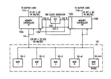
19 Figure 2 is a block diagram depicting one embodiment
of Memory Array 101 as controlled by Memory Controllers 102A
21 and 102B. Memory Array 101 includes Memory Array Boards 101-1
22 through 101-N, and spare Memory Array Board 101-N~1. One level
23 of redundancy is achieved by utilizing two memory controllers.
24 Thus, in the event Memory Controller 102A fails, Memory
Controller 102B is still available. In one embodiment N=4, and
26 each memory array board comprises one gigabyte, arranged as 64M
27 words, each word having 130 data bits and 20 ECC bits. In one
28 embodiment, these 150 bits are arranged in thirty groups of 5
29 bits. The 20 error code bits allow any two groups of five
bits to fail (i.e. a maximum of ten failed bits between two
31 groups), while allowing proper on-the-fly error correction.
32 Alternatively, a single five bit group can fail, together with
33 another single bit error, with all of these errors being
34 correctable by the ECC. Since the memory modules were selected
to be of five bits in width, two memory modules may fail
36 completely and still have their ten data bits corrected by the
37 unique error correction code of this invention. This allows
38 two memory modules to fail for any reason whatsoever, including
WO94/186~ ~14 4 g 8Q PCT~S93/0861 ~
1 failures in address information applied to the "failed" memory
2 modules. It will be appreciated to those of ordinary skill in
3 the art in light of the teachings of this invention that other
4 numbers of error code bits can be used to provide a desired
level of error detection and correction for given memory module
6 sizes, without departing from the spirit of this invention.
8 Spare Memory Array Board 101-N+l is used as
9 replacement when a standard Memory Array Board 101-1 through
101-N is determined to have uncorrectable errors, or
11 correctable errors exceeding a predetermined threshold level.
12 In one embodiment, a simple algorithm is used to cause the
13 error logger to track the number of "hard error" bits (i.e.
14 bits which are permanently in error due to a hardware defect,
rather than a "soft error" in which a properly functioning bit
16 storage area stores an incorrect logic state due, for example,
17 to alpha particle hits) that have occurred on a single memory
18 array board 101-1 through 101-N. In this embodiment, if two or
19 more hard errors have occurred on a single memory array board,
a hot swap operation is initiated to place data from the
21 defective memory array board to the spare memory array board
22 101-N+1. Upon completion of the hot swap operation, the
23 defective memory array board is logically replaced with the
24 spare memory array board 101-N+l, with the defective memory
array board now serving as the spare memory array board in the
26 event another one of the memory array boards becomes more
27 defective than the logically replaced defective memory array
28 board prior to the physical replacement of the defective memory
29 array board.
31 This allows spare Memory Array Board 101-N+l to be swapped
32 on the fly without performance penalty and prior to the
33 defective memory array board becoming so defective as to have
34 uncorrectable errors. Upon such occurrence, service processor
106 (Figure 1) preferably calls the service organization
36 indicating a memory board needs to be replaced at a convenient
37 service time, while in the meantime spare Memory Array Board
38 101-N+1 is hot swapped with the bad Memory Array Board. This
~ 094/18622 21~ ~ 9 8 ~ PCT~S93/08611
1 hot swap may be accomplished in the following manner. First,
2 service processor 106 will determine that a good spare board
3 101-N+l exists and is available as a replacement for the bad
4 Memory Array Board. Service processor 106 then sends a command
to memory controller 102A and memory controller 102B to perform
6 all of their writes to the failed Memory Array Board in
7 parallel with writes to the replacement memory Array Board 101-
8 N+1. Then service processor 106 instructs either memory
9 controller 102A or memory controller 102B to perform a read,
correct, and restore operation for all data locations within
11 the failed Memory Array Board. This, due to the previous
12 instruction to write data in parallel to the spare Memory Array
13 Board 101-N+1, will cause the spare Memory Array Board 101-N+l
14 to become filled with valid data, at which time service
processor 106 instructs memory controllers 102A and 102B to
16 cease accessing the failed Memory Array Board and access spare
17 Memory Array Board 101-N+1 in its place.
18
19 Clock 115A is one of three clocks contained in the
system for maintaining redundancy and clock synchronization.
21 Clock 115A controls the timing of the various registers
22 contained in Memory Controller 102A. Clock Circuit 115A
23 operates as a signal-controlled clock which is synchronized to
24 identical Clock Circuits 115B and 115C (Fig. 2). Clock 115A
provides to Memory Controller Board 102A CLKA, CLKB, CLKC clock
26 signals (generated by clock circuits 115A, 115B, and 115C,
27 respectively), as well as a voted clock signal which provides
28 an accurate clock signal in the event one of the three clock
29 signals fails. Within Memory Controller Board 102A, for
circuits which are triplicated for TMR purposes, each of the
31 three triplicated circuits receive one of clock signals CLKA,
32 CLKB, CLKC. For those circuits which are not triplicated
33 within Memory Controller 102A, the voted clock is used.
34
Figure 2a is a block diagram depicting one embodiment
36 of a triple modular redundant refresh system constructed in
37 accordance with the teachings of this invention. The redundant
38 refresh circuitry of this invention functions to synchronize
21~98~
WO94/186~ PCT~S93/08611
1 three independent refresh circuits in a single refresh timer
2 and allows the refresh circuitry to operate when one of the
3 three independent refresh circuits is defective or removed for
4 repair or replacement. Memory controller 102A includes clock
115A, memory controller 102B includes clock 115B, and clock
6 115C is used to provide the third of the triple modular
7 redundant clocks, as discussed above with reference to Figure
8 2. Associated with clock 115C is one of three TMR refresh
9 generators 1201C, with the other two TMR refresh generators
1201A and 1202b being formed as part of memory controllers 102A
11 and 102B, respectively. Clock 115C feeds its clock signal to
12 refresh counter 1203 and refresh state machine 1202 of refresh
13 generator 1201C. The clock signal from clock 115C is also
14 applied to clocks 115A and 115B, and clock 115C receives clock
signals from clocks 115A and 115B, as described above to
16 provide voted clocks as needed. Refresh counter 1203 serves to
17 maintain a count indicative of when refresh should take place.
18 The output signal from refresh counter 1203 is applied to
19 refresh generators 1201A and 1201B, and refresh counter 1203
receives a refresh count signal from refresh generators 1201A
21 and 1201B. In each refresh generator 1201A, 1201B, and 1201C,
22 a voter such as voter 1204-3 performs a two out of three vote
23 of the three refresh counter signals, with the voted result
24 being applied to refresh counter 1203 in order to determine the
proper interval between refreshes, and to refresh state machine
26 1202 in order to provide refresh re~uest and refresh RAS and
27 refresh CAS signals that are synchronized with the other two
28 refresh circuits. Memory controllers 102A and 102B each
29 include A, B, and C timing generators 1205A,1206A; 1205B,1206B;
and 1205C,1206C, respectively. Each timing generator within
31 each memory controller 102A, 102B receives one of the three
32 clock signals, and provides triplicated busy signals from the
33 memory timing generators indicating that a refresh is not to be
34 performed at this time. These busy signals are voted on by
voters 1204-1 and 1204-2 within refresh generators 1201A,
36 1201B, and 1201C to provide a triple redundant voted indication
37 of whether memory controllers 102A and 102B are busy. Each
38 refresh memory generator provides triple redundant REFRESH
094/18622 2 1 ~ PCT~S93/08611
1 REQUEST, REFRESH RAS, and REFRESH CAS signals, which are
2 applied to the memory array boards 301-1 through 301-60, as is
3 described below with reference to Figure 3.
Figure 2b is a schematic diagram of one embodiment of
6 a triple redundant clock system constructed in accordance with
7 the teachings of this invention. Clock circuit 115C receives
8 a clock signal CLKA and CLKB from clock circuits 115A and 115B,
9 and provides a clock signal CLKC to clock circuits 115A and
115B, as described above with reference to Figure 2. Each
11 clock circuit 115A, 115B, and 115C provides a clock signal
12 synchronized with the other two clocks. This assures two
13 synchronized clocks will be available, even if one of the three
14 redundant clocks fail. This allows a voted clock signal to be
provided based on a vote of two of the three clock signals,
16 ensuring a reliable clock signal even in the event one of the
17 three clock signals is faulty. Clock signals CLKA and CLKB are
18 applied to AND/OR circuit 1151, as is CLKC. AND/OR circuit
19 1151 provides a single voted output signal to drive the clock
circuitry of clock circuit 115C, which is applied to inverter
21 1152. The output signal of inverter 1152 is applied to one
22 side of crystal Y1, which is bypassed to ground by capacitors
23 C1 and C2. The other side of crystal Y1 is coupled via
24 resistor R1 to the voltage divider formed by resisters R2 and
R3, which serves to establish a known fixed output voltage
26 level in the event clock circuit 115C fails. This provides a
27 definitive error condition, which can be detected with
28 certainty. Resistor Rl establishes the symmetry of the CLKC
29 signal, in order to provide a desired duty cycle of
approximately 50~. The output side of resistor Rl is also
31 coupled to diode CR3 which is coupled in series with capacitor
32 C3 to ground. Diode CR3 and capacitor C3 serve to ensure that
33 clock circuit 115C begins to oscillate when powered up. The
34 output side of resistor R1 is also coupled to inverter 1153,
which provides a buffered CLKC output signal. This CLKC output
36 signal is also applied to inverters 1155A, 1155B, and 1155C to
37 provide clock signals 40NSCLKA, 40NSCLKB, and 40NSCLKC to
38 AND/OR circuit 1161, which provides a voted two of three output
WO94/18622 2 1 4 4 ~ ~ ~ 12 P~T~S93/0861 ~
1 signal to clock divider circuit 1181 which provides output
2 signals 80NSCLKA and 80NSCLKB and 160NSCLKA and 160NSCLKB for
3 internal controller timing. Refresh controller circuit 1182
4 serves to generate the refresh time period (e.g. approximately
16 microseconds), determine if the memory controllers are busy
6 performing a memory cycle, generate the control signals (such
7 as refresh RAS, CAS, etc) to perform a refresh cycle, and
8 synchronizes the refresh counters of the other two redundant
9 refresh/clock circuits. One embodiment of a refresh controller
circuit 1182 is shown in the schematic diagram of Figure 2c.
11
12 Figure 3 is a block diagram of one embodiment of a
13 memory array board suitable for use as Memory Array Board 101-1
14 (Fig. 2), with the other memory array boards being of similar
construction in this exemplary embodiment. Memory Array Board
16 101-1 includes, in this embodiment, 60 memory modules 301-1
17 through 301-60. Each memory module includes DRAM Memory 314
18 organized as eight rows by five bits, utilizing forty DRAMs
19 each of four megabytes. Each pair of memory modules (e.g.
Memory Modules 301-1 and 301-31) are cascaded into Bank 0 and
21 Bank 1 addresses in order to provide sixteen rows of five bits
22 per DRAM. It will be appreciated by those of ordinary skill in
23 the art in light of the teachings of this invention that the
24 specific memory size, organization, and DRAM sizes used are
capable of a wide variation depending on specific applications
26 and desires, and the configuration described in this
27 specification is by way of example and not to be construed as
28 a limitation of the scope of this invention.
29
The operation of memory modules 301-1 through 301-60
31 are now described with reference to memory module 301-1. In
32 one embodiment, Memory Bus 110 p ovides three copies of the
33 following signals on redundant busses 110A, 110B, and 110C,
34 which form part of memory cor.troller bus 110:
36 13 ADDR address lines
37 3 RSEL DRAM row select lines
38 1 RAS DRAM row address strobe
~ 0941186~ ~ 2 i ~ ~ 9 8 0 PCT~Sg3/08611
1 1 CAS DRAM column address strobe
2 l REFC Refresh CAS
3 1 RE Read Enable
4 1 INH Inhibit Signal
l BSEL Board Select
6 l REFR Refresh RAS
7 l ZOL Bank Select
8 l DIAG Diagnostic bit
9 1 PREINH Preinhibit
11 The 13 address bits will support up to 64 Megabit
12 DRAM chips. These three copies are provided on busses 110A,
13 110B, and 110C, respectively, to each Memory Module 301-1
14 through 301-60 and are received in each memory module by TMR
Voter 310. Voter 310 performs a two-out-of-three vote on each
16 of these address and control bits in order to provide an error-
17 corrected set of address and control bits to Decoder 312, as
18 well as a single bit ZOL signal to select either Bank Zero
19 (e.g. Memory Module 301-1) or Bank One (e.g. Memory Module 301-
31). Address Buffer 311 provides the remaining address bits to
21 select the appropriate DRAM within Memory 314. As will be more
22 fully described later, a unique error correction code is
23 utilized in conjunction with the deselected width of data
24 stored with in each memory module such that the unique error
correction code is capable of detecting and correcting at le~st
26 one complete failure in any one memory module. In one
27 embodiment, the unique error correction code is capable of
28 correcting complete (i.e. 5 bit) failures in two memory
29 modules, and detect many instances of yet another single bit
error in another memory module. Obviously, this embodiment
31 also allows correction of any 5 bit error and correction of any
32 possible simultaneous single bit error. In this manner, the
33 unique error correction code, used in conjunction with memory
34 array modules of appropriate size, allows Voter 310 to correct
any error in any of the 23 address and memory control bits,
36 which errors may have occurred anywhere in the path from their
37 generation at either ~emory Controller 102A or Memory
38 Controller 102B (Fig. 1) through all circuitry and signal paths
WO94/186~ 2 ~ 4 4 9 8 q PCT~S93/0861 ~
1 to Voter 310. This path includes, for example, the backplane
2 in memory board address drivers 320, 321, 322, board
3 connectors, and other buffer/drivers (not shown) which may be
4 required or desired between the Memory Controller 102A or 102B
and Voter 310. Precharge inhibit signal PREINH serves to tell
6 a memory array board that it should cease operation after
7 completing its current task, following which the INH inhibit
8 signal is generated by the memory controller in order to
9 inhibit all operations on that memory array board, allowing it
to be physically replaced. In an alternative embodiment of
11 this invention, physical pins of appropriate length with
12 respect to the length of other pins of the memory array boards
13 are used to generate an inhibit signal during the physical
14 removal/replacement of a memory array board, as is known in the
art.
16
17 In addition to the triplicated signals indicated above,
18 Memory Bus 110 also provides a nonredundant set of signals to
19 each memory array board, as follows:
21 8 Status [0:7] Status bits
22 1 TMREA TMR Address Error Flag
23 1 TMREC TMR Controller Error Flag
24 1 CNDP Precharge Ground
1 VCCAP current limited precharge VCCA
26 1 VCCBP current limited precharge VCCB
27 1 VCCA VCCA
28 1 VCCB VCCB
29
VCCA (and VCCAP) are supply voltages provided by power
31 supply 113A (Figure 1) and VCCB (and VCCBP) are supply voltages
32 provided by power supply 113B (Figure 1). The precharge
33 supplies VCCAP and VCCBP and precharge ground GNDP are applied
34 to each Memory Array Board 101-1 through 101-N+1 via longer
pins so that during the insertion of a memory array board into
36 a powered up system, the precharge voltages are applied to the
37 memory board prior to data signals, to prevent erroneous
38 signals on the data bus, and prior to supply voltages VCCA and
094/18622 2 i 4 ~ d 8 ~ PCT~S93/08611
1 VCCB, to prevent undesirable transitions on the power supply
2 bus. In one embodiment, precharge voltages VCCAP and VCCBP are
3 current limited by a resistor of approximately 0.5 ohms,
4 allowing the memory array board being inserted to be rapidly
precharged without creating noise.
7 Voter 310 puts out three control signals to its
8 associated one 323-1 of the 30 Data Transceivers 323
9 (transceiver 323-1 being associated with the five data bits of
its associated pair of Memory Modules 301-1;301-31) which, in
11 one embodiment, is a 74FCT646 device available from Quality
12 Semiconductor, Inc. These three control signals are the
13 READBUS ENABLE, which serves to allow data to be transferred
14 between bus 110 and memory array board 101-1, WRITE ENABLE,
which serves to disable memory array board 101-1 when another
16 memory array board is being accessed, thereby preventing data
17 switching within memory array board 101-1 to reduce power
18 consumption, and READ CLOCK, which serves as a data strobe
19 signal indicating valid data is available during a read cycle
of memory array board 101-1. As shown in Figure 3, each pair
21 of memory modules 301-1 through 301-60 has an associated data
22 transceiver 323-1 through 323-30, respectively, so that 150
23 data bits are communicated in parallel on bus 110D. In this
24 manner, if voter 310 fails, it only affects its five data bits
which, as previously mentioned, is correctable as the 150 data
26 bits are organized into thirty groups of five bits, failures in
27 any two of which are correctable. In one embodiment, voter
28 310, address buffer 311, and decoder 312 are formed as part of
29 a single integrated circuit 312, such as an ASIC.
31 One embodiment of a portion of a voter circuit
32 suitable for providing a two-of-three vote on a single set of
33 triple redundant input signals is depicted in Figure 3a. The
34 three redundant input signals are labeled SIGNAL-A, SIGNAL-B,
and SIGNAL-C, received on input leads 1301A, 1301B, and 1301C,
36 respectively. Each input signal is applied to the input lead
37 of a Schmitt Trigger 1302A, 1302B, and 1302C, whose output
38 signal is applied to one input lead of NAND gate 1303A, 1303B,
WO94/18622 21 ~ ~ 9 8 0 16 PCT~S93/0861 ~
1 and 1303C, respectively. The other input leads of NAND gates
2 1303A, 1303B, and 1303C are coupled to a logical one signal
3 (VDD), so that the NAND gates operate as inverters to provide
4 an intermediate output signal for testing purposes or other
uses as may be desired. The output signals of Schmitt Triggers
6 1303A, 1303B, and 1303C are applied to AND/NOR gate 1304, which
7 provides a two-of-three voting selection. The output of
8 AND/NOR gate 1304 is applied to masking AND gate 1305, which
9 gates the voted output of AND/NOR gate 1304 based on the select
signal (for example, the select signal used to select the
11 appropriate one of each pair of memory modules, such as pair
12 301-1, 301-31, as described above with respect to Figure 3).
13 This gated signal is applied to inverter 1306, which in turn
14 provides a gated, voted copy of the triple redundant input
signals.
16
17 Figure 4 is a block diagram depicting one embodiment
18 of Memory Controller 102A, as previously described with
19 reference to Figure 2. A memory operation of Memory Controller
Board 102A will now be described. Buffer 450 communicates via
21 Bus lllA with a host in a block mode fashion. During a read
22 operation, for example, a first load of buffer 450 is initiated
23 by the host to load operation code ("op code") and a word
24 count defining the number of words to be read from Memory Array
101 via Memory Controller Board 102A. If desired, parity bits
26 can also be used during this first load. A second load
27 transfers a start address of 32 bits plus, if desired, 8 bits
28 of parity. This provides sufficient information for Memory
29 Controller Board 102A to perform a block read from the start
address for the number of words specified in the word count.
31 By utilizing eight parity bits, rather than the more
32 traditional four bit parity for a 32 bit word, error detection
33 on any combination of 8 bits is accomplished as opposed to
34 simply odd or even parity detection. Memory Controller Board
102A then provides a series of data transfers to the host in
36 order to transfer the block of data beginning at the starting
37 address and continuing for the specified word count. During
38 writing, this operation is reversed so that the host computer
~ 94~186~ ~1~4~ 8 0~ PCT~S93/08611
1 provides a block of data to be stored in memory at the starting
2 address through the specified word count.
4 Following the first and second loads during a memory
operation, buffer 450 temporarily stores the data for routing
- 6 to Word Count Register 415. The start address is stored in
7 Start Address Register 416, and the op code is stored in
8 Command Decode Register/Decoder 417. Four Port Arbiter 418
9 receives input signals defining when Memory Bus 110 is
available to Memory Controller Board 102A. Four Port Arbiter
11 418 receives input signals from Microprocessor 401, Command
12 Decode Register/Decoder 417, and composite signals on leads 420
13 and 421 from Memory Controller Board 102B (Fig. 1) which shares
14 Bus 110 with Memory Controller Board 102A. The composite
signal received on lead 420 indicates when memory controller
16 board 102B is performing a memory operation such as a soft
17 error scrub, refresh, data move, or data saving operation.
18 Lead 421 receives signals from Memory Controller 102B
19 indicating when Memory Controller 102B is performing a read
request or a write request to Memory Array 101. In any of
21 these cases, Memory Controller 102B has gained access tc Memory
22 Bus 110 and thus Memory Bus 110 is unavailable to Memory
23 Controller 102A.
24
The output bus from Command Register/Decoder 417
26 indicates to Four Port Arbiter 418 when Memory Controller 102A
27 is performing a read request or a write request is desired by
28 Memory Controller 102A. Similarly, Microprocessor 401 provides
29 signals to Four Port Arbiter 418 indicating when Microprocessor
401 wants to perform certain operations such as scrub, refresh,
31 data move, and data save. The refresh signal is triplicated,
32 with copies generated by the clock board, memory controller A,
33 and memory controller B, as described above. Four Port Arbiter
34 418 arbitrates these various input signals and provides an
output signal to Memory Timing Generator 423 (which includes
36 clock 115a, timing generators 1205a,b, and c, and refresh
37 generator 1201a of Figure 2a) indicating whether Memory
38 Controller 102A will be granted access to Memory Bus 110.
WO94/186~ ~14 4 9 8 0 18 PCT~S93/0861 ~
1 Memory Timing Generator 423 in turn controls Address Counter
2 Multiplexer 424 and Memory Mapping Circuit 425 pertaining to
3 availability of Memory Bus 110. Memory Array Mapping Circuit
4 425 serves to map addresses to an appropriate Memory Array
Board 101-1 through 101-N (Fig. 2), thereby allowing different
6 memory sizes to be used in the various memory array boards, if
7 desired. In one embodiment Memory Array Map Circuit 425 is a
8 PROM configured by Microprocessor 401 as a lookup table in
9 order to provide a quick map operation.
11 When Memory Bus 110 is available, Memory Controller
12 102A performs the desired memory operation. This is
13 accomplished by loading the most significant bits of the start
14 address stored in Start Address Register 416 into Address
Multiplexer 431 which in turn are fed to Memory Array Mapping
16 Circuit 425 as previously described. The least significant
17 bits of the start address stored in Start Address Register 416
18 are transferred to Address Counter 430, which sequentially
19 counts each memory operation in order to control the desired
block of memory. The word count stored in Word Count Register
21 415 is transferred to Word Counter 432 which counts down to
22 zero with each count of Address Counter 430 in order to
23 determine when an end of block (EOBLK) signal should be
24 generated when the entire memory block operation has been
completed. This EOBLK signal is fed to Memory Timing Generator
26 423 which terminates the controller cycle, communicates to FIFO
27 Buffer Controller 402 that the operation has been completed,
28 and gives up Memory Bus 110.
29
In the event Four Port Arbiter 418 selects Micro-
31 processor 401 as the device which will gain access to Memory
32 Bus 110, Address Counter 430, Address Multiplexer 431, Word
33 Counter 432, and Address Counter Multiplexer 424 operate to
34 select their input signals from Microprocessor 401 rather than
the signals available as input signals from buffer 450. In one
36 embodiment, Four Port Arbiter 418 allows Memory Controllers
37 102A and 102B to operate in an interleaved fashion, for
38 example, toggling between memory controllers 102A and 102B
094/186~ ~ ~ ~9 8~ PCT~S93/08611
1 after 32 byte transfers, thereby enhancing latency among the
2 various hosts.
4 ECC Data Path Circuitry 407 performs high level error
correction of data flowing between Interface Bus lllA and Data
- 6 Bus llOD (which is the data lines of memory bus 110). Any
7 desired error correction technique can be used. In one
8 embodiment of this invention, a unique code as depicted in
9 Table 1 is used. Novel features of this code include the use
of relatively few error correction bits (simplifying hardware
11 design and expense) while allowing the simultaneous correction
12 of two groups of five bits, as well as allowing fast detection
13 and correction of failed data bits by use of a table look-up
14 memory.
16 A number of techniques have been used in the prior
17 art to improve the reliability of data stored in memory
18 systems. The simplest one has been to add a single parity bit
19 to the data word to signify whether there is an even or odd
number of "one" bits across the data word. The next level of
21 complexity involves using a Hamming code which takes the data
22 word and generates a "code word" (also known as check bits")
23 representation of the data. This "code word" is appended to
24 the data word and this combination then is stored in memory.
The Hamming code has an advantage over the parity techni~ue
26 because it not only detected errors but is also capable of
27 correcting a fixed number of errors. The most common
28 implementation of this code in memory systems involves
29 correcting a single bit error and detecting two bits in error
in a single data word. The most complex codes are Reed-Solomon
31 (R-S) error correction codes. These codes are more efficient
32 in detecting and correcting multiple bit and "burst" type of
33 errors in memory. These detection and correction properties
34 are more applicable to data stored on magnetic media such as
hard disks and floppy disks.
36
37 A unique error correction code is used in accordance
38 with the teachings of this invention. This unique error
WO94/186~ 2 1~ ~ 9 ~ ~ 20 PCT~S93/0861 ~
1 correction code combines the properties of the straight Hamming
2 code with the correction capabilities of the Reed-Solomon code.
3 In accordance with one embodiment of this invention, this
4 unique error correction code is structured such that it works
on groupings of five (5) data bits, as in this implementation
6 there are thirty groups of five bits for a total of 150 bits of
7 information. Of these 150 bits of information, 130 bits are
8 user data bits and twenty (20) bits are used for the error
9 correction code word. One implementation of this unique code
offers the ability to correct up to two groups of five bits
11 (total of 10 bits) in the 150 bit memory word. In addition to
12 correcting bits in any two 5 bit groups, it can also detect
13 errors that are located in a third five bit group. In
14 accordance with this invention, this unique error correction
code can be modified to provide different combinations of error
16 correction and detection depending on the reliability needs of
17 the memory system.
18
19 Each of the twenty ECC "check bits" is generated by
taking the "negative" parity of a unique combination of the
21 user data bits. This generation of twenty "check bits" is
22 performed by the ECC circuitry. Table 1 shows the combinations
23 of the user bits that are used to generate each ECC "check
24 bit".
O 94/18622 214 4 9 8 0 PCT/US93/08611
o X X X X X X X
_~ X X X X X X X
N X X X X X X X X
q X X X X X X X
~P X X X X X X
U~ X X X X X X X
~D X X X X X X K X
X X X X X X X X X X
a~ X X X X X X X
C~ X X X X X X X
, X X X X X
_~ X X X X
_~ X X X X
X X X X X X X X X
X X X X X X X X
X X X X X X X X
~D X X X X X X
-- X X X X X X X
X X X X X X X X X ~C
` X X X X X X X X X
~ o o o o o o o o o o ~~
.,1 o o oooooooooooooo
~ ________________
m m m m m m m m m m m m m m m m m
U ~ 0
0 ~ ~ 0 ~ 0
~ a ~ ~ ~ a a a ~ ~ a a a a a a a
W094/186~2 2`14':~980 22 PCT/US93/08611~
o X X X X X X
--i K X X X X X X X X
t~ XX XX XX XX XX
q x X x x x X X X
X X X X X X
Ul XX X X X X
X XXXX X X XX
1` X X X X X X X X X
a~ X X X x X x
a~ X X X X X X X X
,, X X X X X X X X
X X X X X X X X X
XXXX X X XX X
~ X XXX X X XXXXX
d~ X X X X X X X X X X
X X XXX XXXXXX
~D X XXXXX XXXXXXX X
t` XX XX X XXXX X
X X X X X X X X X X X
X X XXXXXXXXX
~1 C81 t~ `1 N t~l t`l ~ '1 r~l ~
~1 00 0 0 0 0 0 0 00 0 0 0 0 0 0 0
p~ _________________
~ ~ m m m m m m m m m m m m m m m m m
.c
U ~ 0 ~ 0
a ~ ~ a c~ ~ ~ a Q ~ C~
~0 94/18622 23 ~ 4.~ 9~ ~ PCT~I~S93/08611
o X X X X X X X X
X X X X X X X
C~ X X X X X X X
~ X X X X X X
dl X X X K X X X X X
It~ X X X X X X X
X X X X X X X
1` X X X X X X X X
C~ X X X X X X
~ X X X X X
_~ X X X X X X
~ X X X X X X X
N X X X X X X X
X X X X X X X
X X X X X
~n X X X X X X x x X
~D X X X X X X X X
~_~ X X X X X X X X X
X X X X X X X X
~ X X X X X ~ X X
~1 00000000000000000
~q _________________
0 ~ m m m m m m m m m m m m m m m m m
U ~ 00000000000000000
00000000000000000
~ Cl c~ a a ~ ~ a c~ ~ a c~ a ~ c~
WO 94~18622 2 i 4 ~ 9 8!0 24 PCT/US93/0861~
o X X X X X X X
--~ X X X X XX X X K
X X X X X XX X X X
X X X X X XX X X
X XXX XX XX
Ul XX XX XX XXXXXX
~D XX XX XXXXXXXXX
t- X X X X X X X X X X X X
a~ X X X X X X X X X
X X X X X X X X X X
_~ X X X X X X
X X X X X X X
N X K X X X X
X X X X X X X X X X
X X X X X X X X X
~n X X x X X X
~D X X X X X X
1~ X X X X X X X
X X X X X X
X X X X X X X
o ~ O ~ N ~ ~r In ~O
''~ OOOOOOOOOOOOOOOOO
~ _ _ _ _ _ _ _ _ _ _ _ _ _ _ _ _ _
~mmmmmmmmmmmmmmmmmm
aa Q Q Q a Q Q a Q Q Q Q aaa Q a
~O 94/18622 2 I i~4~gd - ~ PCT/US93/08611
o X X X X X X X X X X
_I X X X X X X X X X X
N X X X X X X X X X
X X X X X X X X
X X X X X X X X X
U~ X X X X X X X X X X X
D X X X X X X X X X X
r- X X X X X X X X X X
00 X X X X X X X X X X X X
O~ X X X X X X X X X X
.,~ X X X X X X X
~ X X X X X X X
N X X X X X X X
X X X X X X X
X X X X X X X
Ul X X X X X X X
~ X X X X X X X X X
_~ X X X X X X X X
X X X X X X X X
X X X X X X X X X
0 a~ o ~1 ~ ~ ~ u ~ ~ o ~ ~ ~
.,~ OoOOoOOoOOOOOOOOO
~ ______~,__________
al m m m m m m m m m m m m m m m m m
a a a c~ a c~ c~ a ~ a a a ~ a a a ~ a
WO 94118622 21 4 4 3 g û PCTIUS93/086111~
26
o X X X X X X X X X X
_I XXX XXXX XXXXX X
XX X X X X X X X X
X X X X X X X X X X X
X X X X X X X X X X X X
~C X X X X X X X
~D X X X X X X X X X X X
~ X X XX XXXXX
a~ X X X X X X
o~ X X X X X X X
,, X X X X X X X X
X X X X X X X X X
X X X X X X X X X X X
~ X X X X X X X
dl x x x x x x x
X X X X X X
X X X X X X
1` X X X X X
X X X X X X X X X
~ X X X X X X X X
,1 oooooooooooooooo~
~ _________________
~ ~q m m m m m m m m m m m m m m m m m
0 ~ 0
~ a a a ~ a a a a a a a a a a ~ a a
~O 94/18622 ` 214 4 9 8 0 PCT/US93/08611
27
o X X X X X X X X X X
,1 X X X X X X X X X X
X X X X X X X X
X X X X X X X
>
X X X X X X X X
U~ X X X X X X X X X X X X
~D X X X X X X X X X X X
1` X X X X X X X X X X X
a~ X X X X X X X
~ X X X X X X X X
X X X X X X
_, X X X X X X X X
~ X X X X X X X X
'q x x x x x x
X X X X X X
~n X x X x x X X
D X X X X X X X X
_, X X X X X X X X X
~ X X X X X X
` X X X X X X X
~ ooooooooo~,~
~ _________________
~ ~q m m m m m m m m m m m m m m m m m
00000000000000000
00000000000000000
a a a a a a a a a a a a a a a a a
WO 94/18622 ~1~14 9 8 0 PCT/US93/08611
28
o X X X X X X X
_I X X X X X X X
N X X X K X X
~1 X X X X X X X X X
X X X X X X X X X X
Ul X X X X X X
K X X X X
t- X X X X
C~ XXXXX XXX
O~ XXXX XX
~ XXX XXX
~C XX X X X
X XXXXX
X X X X X X
e~' X X K X X
U' X X X X X X X X X
~D X X X X X X X X X X
_~ K X X X X X X X K
CO K X X X X X X X
X X X X X X X X
0 O~ O ~ o
a~ ----------____________
~mmmmmmmmmmmmmmmmmm
~aaaaaaaaaaaaaaaaa
O 94/18622 j ~ 2~ 8 ~PCT/US93/08611
29
o X
X
~ X
e~l X
U~ X
~D X
X
a) X
X
o X
_~ X
_I
X
~ X
_I
_, X
~D
t`
C~
,~
11~ ~ 1` 0 a~ O ~--I N ~ d' Ul ~ 0 0
~ _______________
v a~ m m m m m m m m m m m m m m m
W094/186~ 21~ ~ 9 8 0 30 PCT~S9310861 ~
1 In the general implementation of the memory system,
2 a user data word (up to 130 bits) is sent to an error
3 correction code (ECC) circuit, which can be conveniently
4 provided as an ASIC, for example. This ECC circuit performs a
series of logic operations on the 130 bit data word and forms
6 a 20 bit error-correction code word. This code word is merged
7 with the 130 bit user data to form a 150 bit memory word. This
8 memory word is then written into the memory store, which is
9 typically made up of a plurality of DRAM devices. Upon readin~
the memory word from the memory store, the 130 bit user data
11 portion is sent to the ECC circuitry where a new error-
12 correction code word is generated. This new error-correction
13 code word is then compared with the 20 bit error-correction
14 code which was read from the memory store. This comparison
results in a code word containing what is referred to as 20
16 "syndrome bits". The syndrome bits are decoded and indicate
17 the reliability status of the memory word read. There are
18 three major status - 1. no errors detected, 2. correctable
19 errors, 3. detected, but not correctable errors. (Note: There
is a small class of data errors which belong in "status 3" but
21 are miscoded into classes 1 or 2. The size of this class
22 depends on the error-correction code).
23
24 Error Logger 438 receives signals from Memory Timing
Generator 423 and ECC Data path circuitry 407 in order to
26 correlate memory addresses with errors detected by ECC Data
27 Path Circuitry 407 and to store this data in real time. The
28 information stored in Error Logger 438 is available to
29 Microprocessor 401 when requested by Microprocessor 401 to
perform error analysis when time permits. Microprocessor 401
31 also serves to initiate a configuration, for example, by
32 determining the size of memory array boards 101-1 through 101-N
33 (Figure 3) forming Memory Array 101, and programming Memory
34 Mapping Circuitry 425 as required based upon memory array board
sizes and number. Microprocessor 401 also serves to perform a
36 memory scrubbing operation in which soft errors in the data
37 stored in Memory Array 101 are determined and correctly
38 rewritten. This is performed by reading addresses in Memory
094/18622 31 PCT~S93tO8611
1 Array 101 sequentially and determining errors made evident by
2 ECC Data Path Circuitry 407. In the event an error is
3 determined, that error is corrected by ECC Data Path Circuitry
4 407 and that address location in Memory Array 101 is rewritten
with the corrected data. These functions of Microprocessor 401
6 pertaining to service processor 106 includes the transfer of
7 information to Service Processor 106 indicating errors detected
8 in Memory Array 101 which cannot be corrected by Memory
9 Controller Board 102A.
11 Microprocessor 401 also communicates to Service
12 Processor 106 indicating when any other errors have been
13 detected in Memory Controller 102A. This accomplishes two
14 purposes. First, if the error is sufficiently detrimental to
memory operation, hosts will be instructed not to access Memory
16 Array 101 via Memory Controller 102A, and their memory
17 operations will be rerouted through Memory Controller 102B
18 (Figure 1). Secondly, an operator is instructed to initiate
19 repairs on Memory Controller 102A. In addition, Memory
Controller 102A communicates to a host via status words upon
21 each memory request initiated by the host as to the status of
22 the memory operation, including uncorrectable errors for which
23 the host may choose to cease accessing Memory Array 101 via
24 Memory Controller 102A. As part of its configuration function,
Microprocessor 401 also serves to Map from a Memory Array Board
26 having a correctable error to the spare board, as has been
27 previously described. Microprocessor 401 also performs
28 diagnostics on Memory Controller 102A and Memory Array 101.
29
Microprocessor 401 also initiates a data save
31 operation, for example, upon complete power failure, in which
32 data stored in Memory Array 101 is transferred to non-volatile
33 media 125A (Fig. 1). Microprocessor 401 also initiates the
34 restore operation, for example, when power is restored, and
data stored in non-volatile media 125A during the data save
36 operation is to be replaced in Memory Array 101. Such data
37 save operations may also occur, for example, when archival of
38 memory array data is desired. Memory Operations Monitor 439
WO94/18622 2 ~ ~ ~ 9 8 0 32 PCT~S93/0861 ~
1 monitors the control signals on Bus 110 regardless of the
2 source of these control signals (i.e. either Memory Controller
3 102A or Memory Controller 102B). This allows, for example, a
4 table to be maintained of data which has been changed in Memory
Array 101. This may be useful, for example, for allowing
6 Memory Operations Monitor 439 to continually update the data
7 stored in Non-Volatile Media 125A, for example providing a
8 "trickle in" archival of data from Memory Array 101 to Non-
9 Volatile Media 125A. This allows data to be continually
updated to Non-Volatile Media 125A when Memory Bus 110 is
11 available, without impairing memory performance. Thus, Memory
12 Operations Monitor 439 maintains a list of addresses within
13 Memory Array 101 which have been updated subsequent to their
14 transfer to Non-Volatile Media 125A, thereby providing
consistency between Memory Array 101 and Non-Volatile Media
16 125A.
17
18 Figure 5 is a detailed block diagram of ECC Data Path
19 407, shown together with Buffer 450 and FIFO 406. ECC Data
Path 407 operates in two primary modes, as well as a secondary,
21 diagnostic mode, if desired. In a first mode, data is received
22 from a host for writing into Memory Array 101. In the second
23 mode of operation, data is read from Memory Array 101 and sent
24 to the host.
26 When receiving data from the host, the data is
27 received via Bus lllA and stored in FI~O 406 pending its output
28 to Bus 441 under control of Buffer Controller 402 (Fig. 4).
29 Check Sum Checker 508 serves to calculate a check sum as each
32 bit word in a block transfer is received on Bus 441, thereby
31 accumulating a total check sum for the entire block being
32 transferred. Upon completion of the block transfer, Check Sum
33 Checker 508 compares its accumulated check sum with the check
34 sum sent by the host. If these check sums do not match, Check
Sum Checker 508 notifies the host via bus lllA that the block
36 transfer failed, allowing the host to retry any desired number
37 of times or, after a pre-determined number of failures, cease
38 retrying or switch to the alternate memory controller path for
~ 094/186~ 2 1 4 ~ B~O~- ~ ? PCT~S93/08611
1 accessing Memory Array 101 via Memory Controller 102B. Check
2 Sum Checker 508 also flags Microprocessor 401 (Figure 4) via
3 bus 441 of the check sum error for use by the Microprocessor
4 401 in performing its diagnostics. As each 32 bit word is
received on Bus 441, it is applied to Funnel 507 in order to
6 accumulate a 128 bit memory word plus its associated 32 parity
7 bits. The 128 data bits are applied to ECC Circuit 509 which
8 generates 20 check bits based upon the 128 data bits received
9 from Funnel 507. These 20 check bits, as well as the 128 bit
memory word plus its 32 parity bits, are applied to Memory Data
11 Buffer 506. Memory Data Buffer 506 checks the parity of the
12 memory data word utilizing the 32 parity bits, prior to sending
13 the 128 bit memory word plus the 20 check bits to Memory Array
14 101 via Memory Data Bus llOD. In one embodiment, there are 150
bits sent on the memory data bus: 148 data bits plus two
16 reserved bits capable of being used in any desired manner, such
17 as flag bits or additional error detection bits. This
18 operation is now verified in the following manner. Memory Data
19 Buffer 506 sends the same 150 bits that it sent to Memory Array
101 to ECC Circuit 505 which takes 128 data bits and generates
21 20 check bits using the same tree as is used in ECC Circuit
22 509. ECC Circuit 505 then compares its 20 check bits with the
23 20 check bits generated by ECC Circuit 509. If these two sets
24 of 20 check bits do not match, an error has been detected in
the path between ECC Code Circuit 509 and ECC Circuit 505, most
26 likely in Memory Data Buffer 506. If such an error is
27 detected, ECC Circuit 505 notifies the host of this error,
28 thereby allowin~ the host to retry or redirect to another
29 controller to resend the block, if desired. ECC Circuit 505
also notifies Microprocessor 401 of this error.
31
32 When data is to be read from Memory Array 101 and
33 supplied to the host, the following process is used. A desired
34 memory location is accessed and 148 bits (128 data bits and 20
check bits) are received from Memory Array 101 via Memory Data
36 Buffer 506 and applied to ECC Circuit 505 and ECC Circuit 503.
37 In one embodiment, 150 bits are received, including two
38 reserved bits which can be used as flag bits or additional
WO94/186~ ~14 4 9 g 34 PCT~S93/08611 ~
1 error correction bits. ECC Circuit 505 receives the 128 data
2 bits and generates 20 check bits. These 20 check bits are
3 compared with the 20 check bits received from Memory Array 101
4 and their difference becomes a 20 bit syndrome word provided to
Error Map Memory 504. If the 20 syndrome bits are all logical
6 zeros, no error has been detected. Otherwise, an error is
7 detected and Error Map Memory 504 receives the 20 syndrome bits
8 as a 20 bit address defining which of the 150 bits is in error.
9 Referring to Table 2, a twenty bit syndrome is generated as the
difference between the twenty check bits received from memory
11 array 101, and the twenty check bits generated by ECC circuitry
12 505 based upon the 150 bits received from memory array 101.
13 These twenty bits of the syndrome are more conveniently
14 referred to as a five bit hex word. Each syndrome indicates
which one or more of the 150 bits received from memory array
16 101 is in error. Table 2, for simplicity, shows only those
17 syndromes indicating a single bit error. Errors of more than
18 a single bit (up to a total of two groups of five bits) are
19 indicated by a syndrome which is the exclusive-or of the
syndromes associated with each of those failed bits, if those
21 bits had been single bit errors. In one embodiment of this
22 invention, a lookup table is used which includes a selected
23 subset of the syndromes associated with single and multiple bit
24 errors, to provide a lookup table of manageable size which
provides the desired levels of error detection and correction.
TABLE 2
Word Bit Syndrome Word Bit Syndrome Word Bit 8yndrome Word Bit Syndrome
[] 94AC6 [8] 94063 [16] 53A98 [24] D4351
[1] 4A563 [9] 4A2B5 [17] 29D4C [25] 7588C
[2] 84235 [10] 7E989 [18] B5CA6 [26] 3AC46
[3] 4239E [11] 9B4DO [19] 5FEC3 [27] BC423
[4] 211CF [12] EC868 [20] F6BCA [28] FF295
[5] EB718 [13] D26A4 [21] 7B5E5 [29] DB95E
[6] D498C [14] 6C3C2 [22] 9CA76 [30] 9E458
[7] 6A4C6 [15] A7039 [23] EA7AB [31] EE02C
Word Bit Syndrome Word Bit Syndrome Word Bit Syndrome Word Bit Syndrome
[32] D3286 [40] 82501 [48] 39968 [56] 526DD ~
[33] 69943 [41] 44094 [49] B8E24 [57] 2C17A OO~r
[34] 90CB5 [42] 2204A [50] OF8C9 [58] B222D
[35] 7D313 [43] 11025 [51] A3C70 [59] 59392
[36] 9A99D [44] 08A96 [52] 54EA8 [60] 849DC
[37] E94DA [45] 8E552 [53] 2F7C4 [61] 424EE
[38] D586D [46] E60A9 [54] B69E2 [62] 242E7
[39] 6AEB2 [47] 732DO [55] A48B3 [63] 123F7
WO 94/18622 PCT/US93/08611_
~1449~ 36
0
o
CO o
a ~ m a~ c ~:
a ~ m ~ a a ~
~ C) ~ N ~ ~ t` ~ O 00 ~ ~ a
~,~ ~ ~ ~ a N ~ C ~ O
~c ~ ~ ~ ~ ~ ~ ~ ~ m o _I N ~ ~ Lt) ~ t`
oo ~n O _I N ~ ~r u7 N N N N N N N N
O
o B
P1 ~
u~ o
t` ¢ IS) ~ IS d' N 00 ~ ~ V 1~ ~ N
rl N ~r .¢ ~ ~1 a, O ^1 N ~ a ~ a~ f7 N C.)
--~ m N ~ ~r U~ ~O t` CO
O
O
P ~
~q O
i~ ~ t'l ~ O a~d~ N ~-1 0 1~ 4 m ~,
i3 ~ ~;4 ~I N ~ IS) O 1: 00 ~r N r~ 3 Lr
~,l n , ~D N al O CO IS) b1 N ~D ~ 1 ~1 0 0 1~
m a ~ a~ a ~ tJ~ ~r to cn ~ N _l o .¢ In ~ D
~a
:~ ~ ~ ~ ~ ~ ~ ~ ~ m ~ tO t~ O ,,
N t~l ~ In ~D 1~ t o a~ o o o o o o ,~ ,
0 ~ ~ ~ ~ ~ ~ '-- ~ h
~3 0
O :~
~o
:4 rJ ~ t~ n ~ 4 m a~ ~: a N tJ~
~ T ~ N -1t~ ) ~ 'a ~ ~ ~ t` m N tJ~ ~
m L` ~ r N m ~ o to ~
tS~ ~ t~1 ~ N C~ ) t` t~ ~1 ~ O t~O a
o C~ ~ t`~ ~, t ~ ~ ~q ~ t~ ~ t~, ~ t~
tq
~ m ~ ~ ~ ~ o ~I N tr~ ~
S-l d' Ir) ~Sl r- t~o t~ o ~ ~ C0 tJ~ O O O O
o ~ ~ atJ~ t~ tJ~ ~ ~( ~1 ~1
B
~V0 94/18622 37 21 ~ q 9 8 0
o
s.~ o o ~ ~ ~ ~1
_I o o o o
~:oooooo
P~oooooo
to o o o o o o
m ~
o
o
o o o o O o O o
O O O O O O OD ~
o 0 0~ O O
o ~ ~ o o o o
~n o o o ~ ~ o o o o
m ~ o ~
o
~ a ~ o o o o o o
oooooo
oooooO
O O O O O~
~ ~1 0 0
m oo a~ o ,~
o
WO94/18622 ~ 1 4 4 9 ~ ~ 38 PCT~S93/0861 ~
1 ECC Correction Circuit 503 then corrects the
2 erroneous bits and provides the corrected bits in 32 bit words
3 plus 8 parity bits for each 32 bit word. This output is
4 provided to bus 441, allowing Check Sum Generator 501 to
generate a Check Sum for each 32-bit word received for an
6 entire block being transferred from Memory Array 101 to the
7 host, and provides the cumulative check sum to the host upon
8 completion of the block transfer from Memory Array 101. The 8
9 bit parity is also sent to the host. Simultaneously, these 32
bits of data and 8 bit parity are sent to FIF0 502 and then to
11 Funnel 507 for the assembly of 128 bit memory words and 32
12 parity bits. The 128 data bits are applied to ECC Circuit 509
13 which generates 20 check bits which are compared with the
14 accumulated 20 bit check bits from ECC Circuit 503. If these
two sets of 20 check bits match, no error has been detected.
16 Conversely, if there is a discrepancy between these two sets of
17 20 check bits, ECC Circuit 509 has determined that an error
18 exists in the path between and including ECC Correction Circuit
19 503 and ECC Circuit 509 (i.e., ECC Correction Circuit 503, FIFO
406, FIFO 502, Funnel 507, ECC Circuit 509, and Check Sum
21 generator 501 and the buses therebetween). If such an error is
22 detected, the host is notified so that the block may be retried
23 or redirected. In one embodiment ECC Circuit 505 notifies
24 Microprocessor 401 when an error has been detected, allowing
Microprocessor 401 to collect statistics for diagnostic
26 purposes. Similarly, Error Map Memory 504 provides an output
27 signal indicating, based upon its decode of the 20 syndrome
28 bits, which one or more bits in the 128 bit memory word are in
29 error.
31 Figure 6 is a more detailed block diagram of one
32 embodiment of Microprocessor 401. Microprocessor 401 includes
33 CPU 660, EEPROM 661, and Local Bus Decoder 663 communicating
34 via Local Bus 665. CPU 660 also communicates via Local Bus 665
to one or more Reset Control Ports 662 which serve to reset
36 state machines, processors, and registers to known states upon
37 reset, as is known in the art. Service Processor Interface 440,
38 which in turn communicates with Service Processor 101 (Fig. 1).
~ 094/186~ i,2 1~4~.4~ PCT~S93/08611
39
1 Local Bus to Peripheral Bus Buffer 664 allows communicatlon
2 between Local Bus 665 and Peripheral Bus 667. For convenience,
3 Local Bus 665 and Peripheral Bus 667 are shown simply as
4 Microprocessor Access Bus 481 in Figure 4, and may be formed as
a single bus in an alternative embodiment. Microprocessor 401
6 also includes ECC Control/Status Port 607 which communicates
7 between Peripheral Bus 667 and ECC Data Path 407 (Fig. 4).
8 Peripheral Bus 667 also communicates with Memory Timing
9 Generator Control/Status Port 623 which in turn communicates
with Memory Timing Generator 423 (Fig. 4). Miscellaneous Ports
11 Register 672 serves to allow communication between Peripheral
12 Bus 667 and various miscellaneous registers contained within
13 Memory Controller 102A (Fig. 4). Error Logger 438 (Fig. 4) is
14 also coupled to Peripheral Bus 667 allowing communication
between Error Logger 438 and CPU 660. Memory Map Interface 635
16 allows communication between Peripheral Bus 667 and Memory
17 Mapping Circuitry 425 (Fig. 4). Buffer Interface Control
18 Status Port 609 allows communication between Peripheral Bus 667
19 and Buffer Controller 407 (Fig. 4). As shown in Figure 6,
Memory Operations Monitor Interface 439 is also coupled to
21 Peripheral Bus 667, as is CPU to Memory Bus Interface/Port 669,
22 allowing communication between Peripheral Bus 667 and Memory
23 Interface Data Bus 441 (Fig. 4). In one embodiment, Data Save
24 Circuitry 405 includes two separate channels, each including a
SCSI Data Funnel 670-1, 670-2 and a SCSI Interface 671-1, 671-
26 2. Each Data Funnel 670-1, 670-2 is coupled to Memory
27 Interface Data Bus 441 for communication with its associated
28 SCSI Interface 671-1, 671-2. SCSI Interfaces 671-1 and 671-2
29 are coupled to Peripheral Bus 667 and to their associated mass
storage device (or string of devices) 125A-1 and 125A-2,
31 respectively. Microprocessor 401 serves to perform diagnostics
32 and monitoring of the operation of Memory Controller 102A, and
33 configuration of Memory Controller 102A, and the data save
34 archival operation.
36 All publications and patent applications mentioned in
37 this specification are herein incorporated by reference to the
38 same extent as if each individual publication or patent
WO94/186~ 2 1~ 4 9 8 0 PCT~S93/0861
1 application was specifically and individually indicated to be
2 incorporated by reference.
4 The invention now being fully described, it will be
apparent to one of ordinary skill in the art that many changes
6 and modifications can be made thereto without departing from
7 the spirit or scope of the appended claims.