Note: Descriptions are shown in the official language in which they were submitted.
214 01'~
_ 1 ~_
CELL MULTIPLEXER HAVING CELL DELINEATION FUNCTION
BACKGROUND OF THE INVENTION
The present invention relates to a cell
multiplexes and particularly relates to a cell
multiplexes having a "cell delineation" function in
which: relatively low-bit-rate fixed-length packets
(cells) of an asynchronous transfer mode (hereinafter
referred to as "ATM") received from subscriber lines
are stored in a buffer memory; and boundaries between
cells are identified so that correct data blocks thus
read are transmitted to an output line.
As a conventional cell multiplexes, there is
known a structure having cell delineation circuits
corresponding to respective lines for performing cell
multiplexing after cell synchronization, for example,
as disclosed in "Discussion of A Header Error Check
Calculation Circuit" reported in the Institute of
Electronics, Information and Communication Engineers,
1990 Spring National Conference, Japan.
According to the conventional structure,
however, one cell delineation circuit can process a
signal in only one input line, so that a plurality of
cell delineation circuits are required correspondingly
to respective input lines even in the case where the
transmission bit rate in the lines is low. For
example, in the case of a system in which input line
21450~.'~
- - 2 -
signals transmitted at the bit rate of about 6.3 mega-
bits per second are transmitted to the ATM switch side
while 21 input lines are multiplexed, 21 cell delinea-
tion circuits are required. In addition, the conven-
tional structure requires memories for storing cell
signals correspondingly to respective lines for the
purpose of cell multiplexing, so that the hardware size
thereof becomes large.
SUMMARY OF THE INVENTION
An object of the present invention is to
provide a cell multiplexes in which cell signal outputs
can be controlled so that the head of each of data
blocks given to an output line coincides with the head
of a corresponding cell.
Another object of the present invention is to
provide a cell multiplexes in which a buffer memory for
storing input cells temporarily and a read/write
control means can be used to be common to a plurality
of input lines so that data blocks subjected to cell
delineation are read out to an output line.
A further object of the present invention is
to provide a cell multiplexes which is formed so that a
cell delineation control means can be used so as to be
common to a plurality of lines.
To achieve the foregoing objects, according
to an aspect of the present invention, the cell
multiplexes, in which fixed-length cell signals given
~~.45~1~.7
- 3 -
in parallel from a plurality of input lines are stored
in a buffer memory temporarily and then sent out to an
output line in the form of data blocks synchronized
with a predetermined cell structure, comprises a
multiplexing means for multiplexing cell signals
received from a plurality of input lines, a write
control means for storing cell signals outputted from
the multiplexing means in the buffer memory succes-
sively, a read control means for reading the cell
signals stored in the buffer memory in the form of data
blocks each constituted by a predetermined number of
bytes correspondingly to the input lines, and a cell
delineation control means for detecting the delineation
state of each of the data blocks read from the buffer
memory, notifying the read control means of delineation
control information in accordance with a result of the
detection and transmitting data blocks synchronized
with the predetermined cell structure to an output line
selectively, and wherein the read control means
determines the read beginning addresses of data blocks
to be read nextly correspondingly to the respective
input lines on the basis the delineation control
information notified by the cell delineation control
means.
According to an embodiment of the present
invention, the cell delineation control means includes
a table for storing CRC operating data for detecting
the positions of cell headers corresponding to the
21~~~1~
- 4 -
respective input lines and for storing delineation
state information, so that the cell delineation control
means detects the positions of cell headers contained
in respective data blocks read out from the buffer
memory by using the CRC operating data read out from
the table and detects the delineation states of the
data blocks. Further, the cell delineation control
means transits delineation states on the basis of the
detected delineation states and the delineation state
information read out from the table and controls
transmission of data blocks (cell signals) to the
output line in accordance with the delineation states.
According to another aspect of the present
invention, the cell multiplexer comprises: a plurality
of multiplexing units connected to a plurality of input
lines, respectively; a selector means connected to the
plurality of multiplexing units to make data blocks
outputted from the multiplexing units pass selectively;
a cell delineation control means for detecting cell
delineation states of respective data blocks supplied
from the selector unit and generating delineation
control information in accordance with a result of the
detection; and an output control means for designating
multiplexing units to output data blocks in a prede-
termined sequence, and notifying the multiplexing units
of delineation control information received from the
cell delineation control means; and
wherein each of the multiplexing units
214541
- 5 -
includes a multiplexing means for multiplexing ATM cell
signals inputted through the plurality of input lines,
a buffer memory for storing the ATM cell signals
temporarily, a write control means for storing the ATM
cell signals outputted from the multiplexing means in
the buffer memory successively correspondingly to the
lines, and a read control means for reading the ATM
cell signals stored in the buffer memory in the form of
data blocks each constituted by a predetermined number
of bytes correspondingly to the lines, wherein the read
control means determines read beginning addresses to
read data blocks nextly correspondingly to the lines.
According to a further aspect of the present
invention, the cell multiplexes comprises a multiplex-
ing means for multiplexing signals inputted through a
plurality of input lines, a memory for storing the
input signals temporarily, a write control means for
storing the input signals outputted from the multiplex-
ing means in the memory correspondingly to the input
lines, a read control means for reading the input
signals stored in the memory in the form of data blocks
each constituted by a predetermined number of bytes
correspondingly to the input lines, a cell delineation
control means for detecting the delineation state of
each of the data blocks read from the memory, notifying
the read control means of control information in
accordance with a result of the detection and transmit-
ting data blocks synchronized with the predetermined
214~01~
- 6 -
cell structure to the output line selectively, and a
conversion means for converting the respective data
blocks read from the memory into cells each having a
predetermined structure to transmit the cells to the
output line and notify the control information to the
read control means, wherein
the read control means selectively supplies
data blocks read from the memory to either means
selected from the delineation means and the conversion
means in accordance with signal transmission protocol
in the respective subscriber lines and determines read
beginning addresses to read next data blocks corre-
spondingly to the input lines on the basis of the
control information notified by the cell delineation
means and the conversion means.
According to the present invention, one cell
delineation circuit can be used so as to be common to a
plurality of lines and, accordingly, a buffer memory
and a memory controller constituted by a write control
portion and a read control portion as described above
can be used so as to be common to the plurality of
input lines, so that the cell multiplexer can be made
small-sized.
BRIEF DESCRIPTION OF THE DRAWINGS
Fig. 1 is a functional block diagram showing
an embodiment of a cell multiplexer according to the
present invention;
214~0~.7
Fig. 2 is a diagram showing a network system
to which the multiplexes according to the present
invention is applied;
Fig. 3 is a diagram showing the structure of
the memory controller 3 which is one of constituent
elements of the multiplexes according to the present
invention;
Fig. 4 is a diagram showing the format of an
ATM cell;
Fig. 5 is a diagram of transition of cell
delineation state in the ATM;
Fig. 6 is a diagram of transition of cell
delineation state in the ATM;
Fig. 7 is a diagram for explaining methods 1
to 3 employed in the present invention for controlling
read beginning addresses to read data blocks for cell
delineation;
Fig. 8 is a diagram showing the structure of
the cell delineation control unit 4 for carrying out
the data-read beginning address control method 1;
Fig. 9 is a diagram for explaining the
principle of the data-read beginning address control
method 1;
Fig. 10 is a diagram showing an embodiment of
the CRC operation unit 411-a;
Fig. 11 is a diagram showing an operation
sequence in the data-read beginning address control
method 1;
_ 214~0~.'~
_8_
Fig. 12 is a diagram showing an operation
sequence in a modified example of the data-read
beginning address control method 1;
Fig. 13 is a diagram for explaining the
principle of the data-read beginning address control
method 2;
Fig. 14 is a diagram for explaining the
principle of the data-read beginning address control
method 2;
Fig. 15 is a diagram showing the structure of
the cell delineation control unit 4 for carrying out
the data-read beginning address control methods 2 and
3;
Fig. 16 is a diagram for explaining cell
delineation table access timing in the data-read
beginning address control method 2;
Fig. 17 is a diagram showing a second
embodiment of the cell multiplexes according to the
present invention;
Fig. 18 is a diagram showing a third
embodiment of the cell multiplexes according to the
present invention;
Fig. 19A is a diagram showing a first type
cell structure generated by the aforementioned cell
multiplexes;
Fig. 19B is a diagram showing a second type
cell structure generated by the aforementioned cell
multiplexes;
21~50~~
_ g _
Fig. 19C is a diagram showing the contents of
the sixth byte in each of the aforementioned cells; and
Fig. 20 is a diagram showing the detailed
structure of the AAL1 processing unit depicted in Fig.
18.
DESCRIPTION OF THE PREFERRED EMBODIMENTS
Fig. 2 shows an example of an ATM network
system to which a cell multiplexes according to the
present invention is applied.
In the drawing, the reference symbol A (A-1
to A-m) designate cell multiplexers, B subscriber
terminals for transmitting/receiving information such
as voice information, image information, data infor-
mation, or the like, in the form of fixed-length
packets (ATM cells) and C an ATM switch. If cell
signals transmitted from terminals are inputted
directly into the high-speed ATM switch C in the case
where the bit rate in the subscriber terminals is as
low as about 6.3 mega-bits per second, efficiency
becomes very low. Therefore, generally cell signals
from the plurality of subscriber terminals B are
multiplexed by the cell multiplexers A so that
resulting multiplex signals are inputted into the ATM
switch C.
Fig. 1 shows an example of the structure of a
cell multiplexes A-1 according to the present inven-
tion.
2145417
- 10 -
The cell multiplexes A-1 comprises a signal
multiplexes 1, a memory 2, a memory controller 3, and a
cell delineation control unit 4.
The signal multiplexes 1 receives cell
signals (cell data) transmitted from a plurality of
subscriber terminals B, time-divisionally multiplexes
these cell signals, for example, byte by byte and
supplies the resulting multiplex signal to the memory
(buffer memory) 2. Line identification numbers are
given to input lines L (L1 to Ln) connected to the
subscriber terminals so as to be peculiar to the input
lines L, respectively. The signal multiplexes unit 1
has line interfaces (not shown) corresponding to the
input lines. Time-division multiplex cell data
supplied to the memory 2 are provided with line
identification numbers assigned to the line interfaces,
respectively.
Cell signals supplied from the signal multi-
plexes 1 to the memory 2 are stored in the memory 2 so
that the cell signals are managed by a write function
unit 31 of the memory controller 3 in the order of data
arrival in accordance with the respective lines. This
may be achieved by assigning predetermined-capacity
buffer areas corresponding to the lines to write the
cell signals in the buffer areas corresponding to the
input lines or by sharing the memory 2 to a plurality
of lines in the form of a shared buffer in which
addresses of cell signal storage areas are chained in
214501'
- 11 -
accordance with the lines.
As shown in Fig. 3, the memory controller 3
includes a write function unit 31 for recording cell
signals inputted by means of time-divisional multi-
plexing into the memory 2 in the form in which the
order of arrival is managed correspondingly to the
respective lines, and a read function unit 32 for
reading the cell signals stored in the memory 2
successively from data-read beginning positions
recorded correspondingly to the respective lines in
advance and transmitting one-cell data blocks to the
respective lines successively.
The write function unit 31 has a write
controller 311, and a write address table 312 which
stores write addresses 312B of the memory 2 corre-
spondingly to line identification numbers 312A.
A line identification number extracted by the
signal multiplexes 1 is inputted to the write control-
ler 311, so that a write address corresponding to the
line identification number is read from the write
address table 312. A cell signal supplied from the
signal multiplexes 1 to the memory 2 is written into a
position indicated by the write address. Whenever a
cell signal is written, the value of the write address
is updated so that a next cell signal which will come
through one and the same line is written in a position
continued to the write position of the current cell
signal, and this value is stored in a corresponding
214~0~.'~
- 12 -
write address 312B within the write address table 312.
The read function unit 32 has a line
designator 321, a read address table 322 for storing
read beginning addresses 322B to begin reading of data
blocks correspondingly to the line identification
numbers 322A, a read address controller 323, a read-
data length counter 324, and a read address
displacement controller 325.
The line designator 321 checks the read
address table 322 and the write address table 312 while
circulatively changing the line identification number
to read the cell signal, obtains the quantity of data
stored in the memory 2 on the basis of difference
between the write address 312B and the read address
322B in each line, finds line identification numbers
permitting cell signals to be read and notifies the
line identification numbers to the read address
controller 323. Reading of cell signals is carried out
with respect to the line in which the data block size
reaches a value designated by the read-data length
counter 324.
The read address controller 323 picks out a
read beginning address 322B corresponding to the line
identification number designated by the line designator
321 from the read address table 322, reads data of a
block size designated by the read-data length counter
324 from the memory 2 by using the read address as the
top of the data block and transmits the data to the
2145017
- 13 -
cell delineation control unit 4. When a data block is
read from the memory 2, a corresponding line number is
notified to the cell delineation control unit 4 from
the line designator 321.
The read address displacement controller 325
determines a read beginning position to read the next
data block in a corresponding line after one-block data
are read from the memory 2. The read beginning address
to read the next data block is determined in accordance
with the cell delineation state of the precedingly read
data block, so that the displacement of the address is
obtained in accordance with the cell delineation state
signal given from the cell delineation control unit 4
and is given to the read address controller 323.
The read address controller 323 adds the
aforementioned displacement to the current read address
stored in the read address table 322 and stores the
resulting address as the next read beginning address in
the read address table 322.
The following describes the cell delineation
state in the ATM network.
To make the state of a data block read from
the memory 2 a "cell delineation" state coincident with
the ATM cell structure, it is necessary to detect the
header error check (HEC) portion of the ATM cell. The
HEC portion is provided for detection of the top of the
ATM cell constituted by a 53-byte fixed-length data
block, error detection and error correction in the cell
_ 214017
- 14 -
header, and so on. For example, as shown in Fig. 4,
the ATM cell has an ATM cell header H1 with a size of 4
bytes at the top of the cell. A CRC operation result
obtained with respect to this cell header H1 is set in
the fifth byte of each cell as the HEC portion H2.
Figs. 5 and 6 show the transition of cell
delineation state.
The cell delineation state is internationally
standardized in accordance with CCITT I.432.
"HUNT" S11 shown in Fig. 5 represents a
hunting state in which there is no HEC portion
detected. When some HEC portion is detected in this
state, the state is transitted to a "PRESYNCH" state
S12.
As long as the state is "PRESYNCH" S12, there
is monitored whether the next HEC portion is located in
a position (expected position) one-cell distant from
the detected HEC position or not. When the next HEC
portion cannot be detected in the expected position,
the state is transitted to the "HUNT" state S11 again.
When the next HEC portion can be detected in
the expected position, the monitoring of the HEC
portion is performed continuously in the same manner as
described above so that the number of times of continu-
ous detections is measured as the number of protection
stages. When the number of protection stages exceeds a
predetermined threshold value, the delineation state is
transitted to the "SYNCH" state S13.
2145~1'~
- 15 -
As long as the state is "SYNCH" S13, there is
monitored whether the HEC portion is located in a posi-
tion one-cell distant from the detected HEC position or
not, in the same manner as in the "PRESYNCH" state 512.
When the next HEC portion cannot be detected, the
monitoring of the HEC portion is continued so that the
continuous non-detection number of times is measured as
the number of protection stages. When the number of
protection stages exceeds a predetermined threshold
value, the delineation state is transitted to the
"HUNT" state S11.
"Detection Mode" S21 shown in Fig. 6 is a
mode in which error correction is not carried out even
in the case where error is detected in the cell header.
"Correction Mode" S22 shown in Fig. 6 is a mode in
which error correction is carried out by using the HEC
portion in the case where there is one-bit error in the
header.
If there is no error in the cell header of a
cell received in the "Detection Mode" S21, the mode is
transitted to the correction mode S22. If there is
contrariwise some error detected even in one bit of the
cell header of a cell received in the correction mode
S22, the mode S21 is transitted to the detection mode
S21 (after error correction in the case of one-bit
error). These "Detection Mode" and "Correction Mode"
have a relation with idle cell generation control which
will be described later.
_ 214~01'~
- 16 -
Fig. 7 shows relations between data block
size designated by the read-data length counter 36 and
the read beginning address of the next data block
determined by the address displacement controller 325
in accordance with the cell delineation state.
In Fig. 7, there are shown three embodiments
of methods 1, 2 and 3 different in combination of the
data block size and the read beginning address.
In the method 1, the data block size desig-
nated by the read-data length counter 324 is made to be
53 bytes equal to the length of one ATM cell and, in
the case where the cell delineation state is either
"HUNT" S11 or "SYNCH" S13, the read address displace-
ment for designating the read beginning position to
read the next data block is made to be 53 bytes (equal
to the length of one cell). In the case where the cell
delineation state is "PRESYNCH" S12, the read address
displacement is made to be h+53 bytes when the dis-
placement from the top of the read data block to the
top of the cell is h bytes. The top of each cell is 4
bytes short of the detected HEC portion H2.
In the aforementioned "PRESYNCH" state S12,
the following two cases are thought of.
The first case is the case where there is
some difference between the top of the cell and the top
of the data block read from the memory 2 (equivalent to
the read beginning address to read the data block from
the memory 2) just after the state is transitted from
21~~4~.'~
- 17 -
the "HUNT" state S11 to the "PRESYNCH" state 512, that
is, the case of h~0. The second case is the case where
the "PRESYNCH" state S12 has been continued several
times so that the top of the cell coincides with the
top of the read data block, that is, the case of h=0.
In either of the aforementioned cases, a
position one-cell (53 bytes) distant from the top (the
h-th byte position from the read beginning address to
read the data block) of the detected cell can be used
as a read beginning address to read the next data
block.
The address displacement controller 325
obtains address displacement for designating the read
beginning address to read the next data block in each
of the lines on the basis of the cell delineation state
(S11 to S13) notified by the cell delineation control
unit 4 and the value indicating the relative position
of the HEC portion in the data block read precedingly.
In the method 2, the data block size desig-
nated by the read-data length counter 324 is made to be
53 bytes equal to the length of one ATM cell, so that
when the cell delineation state is "HUNT" 511, the read
beginning address to read the next data block is
updated to a value shifted by 49 bytes from the current
value so that the last 4 bytes of the data block read
out precedingly are contained in the leading portion of
the next data block to be read out. When the cell
delineation state is "PRESYNCH" or "SYNCH", the read
_214~~~~
- 18 -
beginning address to read the next data block is
updated in the same manner as in the method 1.
In the method 3, for convenience of cell
processing in other circuits connected as posterior
stages, data blocks are read out so that the top of the
cell is located in the m-th byte position from the top
of each of the data blocks read out from the memory.
When, for example, the data block size designated by
the read-data length counter 324 is 57 bytes which is
larger than the length (53 bytes) of one ATM cell, the
read beginning address to read the next data block is
updated to the (h-m+53)-th byte position from the top
of the preceding data block in a period in which the
cell delineation state is "PRESYNCH", in which: h
represents the leading position of the cell in the
preceding data block; and m represents the target posi-
tion for the top of the cell in the next data block,
each of h and m having a value equivalent to displace-
ment (the number of bytes) from the leading position
of the data block. For example, the value of m is
selected from integers of "1" to "5".
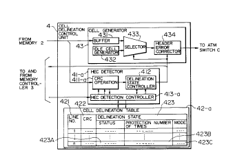
Fig. 8 is a functional block diagram of the
cell delineation control unit 4 for performing cell
delineation in accordance with the method 1. The cell
delineation control unit 4 includes an HEC detector 41-
a, a cell delineation table 42-a, and a cell generator
43.
The HEC detector 41-a which is provided for
_ 2I4~0~.7
- 19 -
detecting the position of the HEC portion of an ATM
cell, is constituted by a CRC (cyclic redundancy check)
operator 411-a, a delineation state controller 412 and
an HEC detection controller 413-a.
The HEC detection controller 413-a performs
controlling of the CRC operator 411-a and the delinea-
tion state controller 412 and performs accessing of the
cell delineation table 42-a which will be described
later.
Because the HEC portion H2 of an ATM cell
indicates a result of the CRC operation of the ATM cell
header H1 having a length of 4 bytes as shown in Fig.
4, it is necessary for detection of the HEC portion H2
that continuous 5-byte data are inputted to the HEC
detector 41-a and that verification is made as to
whether a result of the CRC operation of 4-byte data of
from the first byte to the fourth byte coincides with
the value of the fifth byte or not.
Fig. 9 shows positional relations between
data block and top of cell in two lines identified by
line ID Nos. i and j, respectively, in the case where
cell signal data blocks are read out from the memory 2
in order of a data block R11 of line ID No. i, a data
block R12 of line ID No. i and a data block R13 of line
ID No. i as a simple example.
Pay attention to the cell signal of line ID
No. i, now. Assume that the top of the cell is located
in the 52nd byte (P11) from the leading position of the
- _ 2~~5Q~ 7
- 20 -
data block when the first data block R11 is read out.
Because the HEC portion H1 is located so as to be
shifted by 4 bytes from the top of the cell, the HEC
portion H1 of the cell is located in the third byte P12
from the leading position of the data block R13 which
is to be read out next. It is necessary that the HEC
detector 41-a can detect the HEC portion H1 even in the
case where a cell header is read out over two data
blocks as described above.
As shown in Fig. 10, the CRC operator 411-a
has: a shifter F composed of five flip-flop circuits F-
1, F-2, F-3, F-4 and F-5 which are tandem connected to
one another and operate so that 8-bit cell signal data
read out byte by byte from the memory 2 are transferred
to the rear stage successively; and a CRC operation
checker X1 receiving respective outputs of the flip-
flop circuits and performing CRC operation on the basis
of continuous five-byte data.
The CRC operation checker X1 carries out an
HEC detecting operation on the basis of the CRC opera-
tion value generated at a point of time when four-byte
data equivalent to the ATM cell header H1 are inputted
to the flip-flop circuits F-2 to F-5 and the data value
of the HEC portion H2 following the cell header as
inputted to the flip-flop circuit F-1 and outputs a
control signal indicating a result of the detection.
When only one line is a subject of the HEC
detection, the CRC operator 411-a carries out the CRC
2145 01'~
- 21 -
operation of four-byte data while supplying input
signals to the shifter F (flip-flop circuits F-1 to F-
5) successively to thereby retrieve a position in which
the value of the CRC operation coincides with the last
byte data (HEC). When cell signals inputted through a
plurality of lines are used as shown in Fig. 2, it is
however necessary that a storage area for holding
values (trains of input data) to be set to the flip-
flop circuits and state data generated on the basis of
these input data trains as "CRC operating data" corre-
spondingly to the respective lines is prepared in
advance so that an operation of holding CRC operating
data on the way of processing and an operation of
calling in the preceding CRC operating data in a line
to be subjected to processing are carried out whenever
a data block is switched to a new one, for example, as
R11 is switched to R12 or as R12 is switched to R13 as
in Fig. 9.
Referring back to Fig. 8, the cell delinea-
tion table 42-a stores CRC operating data 422 and
delineation state information 423 correspondingly to
the respective line identification numbers 421. The
delineation state information 423 contains status 423A
indicating any one of "HUNT" state S11, "PRESYNCH"
state S12 and "SYNCH" state S13 shown in Fig. 5,
protection number of times 423B in "PRESYNCH"/ "SYNCH",
and mode 423C indicating either "Detection Mode" S21 or
"Correction Mode" S22 shown in Fig. 6.
21~~417
- 22 -
For example, at a point of time when the
reading of the data block of line ID No. j is completed
and the data block of line ID No. i is to be read out
from the memory 2, the HEC detection controller 413-a
saves the CRC operating data and the delineation state
with respect to line ID No. i onto the cell delineation
table 42-a and reads out the CRC operating data with
respect to line ID No. i from the cell delineation
table 42-a to thereby set a train of data to the flip-
flop circuits in the CRC operator 411-a. Accordingly,
the leading data of a new data block read out from the
memory 2 is supplied to the respective flip-flop
circuits of the CRC operator 411-a so as to follow the
last data of the preceding data block.
From the aforementioned reason, the CRC
operator 411-a has selectors SEL-1 to SEL-5 on the
output side of the flip-flop circuits F-1 to F-5 as
shown in Fig. 10. Each of the selectors SEL-1 to SEL-5
selects either data outputted from the preceding-stage
flip-flop circuit or data given from the HEC detection
controller 413-a in accordance with the control signal
generated from the HEC detection controller 413-a and
supplies the selected data to the CRC operation checker
X1 and the next-stage flip-flop circuit. The input
selection of the selectors SEL-1 to SEL-5 controlled by
the HEC detection controller 413-a will be described
later with reference to Fig. 11 which is a time chart
of a sequence.
2~.4~417
- 23 -
The delineation state controller 412 performs
management of state transition among states S11, S12
and S13 shown in Fig. 5, management of protection
number of times in "PRESYNCH" state S12 and "SYNCH"
state S13 and management of state transition between
"Detection Mode" S21 and "Correction Mode" S22 shown in
Fig. 6.
When the data block (cell signal) of line ID
No. i is read out from the memory 2, the HEC detection
controller 413-a transfers the delineation state 423 of
line ID No. i read out from the cell delineation table
42 to the delineation state controller 412. The
delineation state controller 412 transits the delinea-
tion state on the basis of the delineation state 423
received from the HEC detection controller 413-a and
the control signal given from the CRC operator 411-a.
When the data block read out from the memory
2 is switched from line ID No. i to line ID No. j., the
delineation state stored in the delineation state
controller 412, as well as the aforementioned CRC
operating data, is held in the line ID No. i record of
the cell delineation table 42-a. In this occasion, the
delineation state and a header error correction signal
are transmitted from the delineation state controller
412 to the cell generator 43 whereas the delineation
state and a signal indicating the position of the HEC
portion H2 are transmitted from the delineation state
controller 412 to the memory controller 3. As a
_ 214027
- 24 -
result, the read address displacement explained above
with reference to Fig. 7 is controlled.
The cell generator 43 has a buffer 431 for
storing cell signals read out from the memory 2
temporarily, an idle cell generator 432, a selector 433
for selecting either cell outputted from the buffer 431
or idle cell generated by the idle cell generator 432,
and a header error corrector 434 for correcting error
when error occurs in the header of the cell passing
through the selector 433.
The cell generator 43 operates to suppress
the data block (cell signal) read out from the memory 2
from being transmitted to the output line and transmit
the idle cell generated by the idle cell generator 432
to the output line by controlling the selector 433 on
the basis of a control signal issued by the HEC
detector 41 in accordance with the state of the fifth-
byte data (HEC portion H2) in each data block (ATM
cell) in a period of "HUNT" state S11 or "PRESYNCH"
state S12 or when incorrectable error is detected in
the header in the "SYNCH" state S13.
When there is no error in the header in the
"SYNCH" state S13, the cell signal read out from the
memory 2 is made to pass. When there is some correct-
able error in the header H1 in the "SYNCH" state S13,
error correction is performed by operating the header
error corrector 434 and then the cell signal is
transmitted to a cell processing circuit.
2145417
- 25 -
The buffer 431 is provided to temporarily
buffer cell signals read out from the memory 2 until a
control signal comes from the HEC detector 41-a, that
is, the buffer 431 outputs input cell signals succes-
sively in the form of FIFO (first-in first-out).
Fig. 11 shows a cell delineation control
sequence using the method 1 at the time of the reading
of a cell signal R22 of line ID No. j, in the case where
data blocks (cell signals ) R21, R22 and R23 received
from line ID Nos. i, i and k are to be read out from
the memory 2 successively.
While the data block R21 of line ID No. i is
read out from the memory 2, a signal indicating the
line ID No. i of the next data block to be read out is
transmitted from the memory controller 3 to the HEC
detection controller 413-a (j-21). The HEC detection
controller 413-a reads out CRC operating data 422 and
delineation state information 423 concerned with the
line ID No. ,I from the cell delineation table 42-a on
the basis of the aforementioned signal (j-22).
The HEC detection controller 413-a switches
the selectors SEL-1 to SEL-5 to set CRC operating data
(a train of data in the last portion of the preceding
data block) concerned with line ID No. j_ and having
been already read out from the cell delineation table
42-a to the flip-flop circuits F-1 to F-5 at the timing
of the leading of data block R22 when the data block to
be read out from the memory 2 is switched from data
- m4~o~~
- 26 -
block R21 of line ID No. i to data block R22 of line ID
No. j.. At this point of time, the HEC detection con-
troller 413-a holds a train of data of line ID No. i
fetched from the respective flip-flop circuits tempo-
s rarily. The train of data is stored as CRC operating
data 422 of line ID No. i in the cell delineation table
42-a in suitable timing (i-25) in a period in which the
next data block R22 is processed.
In the timing in which the first data in the
next data block R22 is read out, the selectors SEL-1 to
SEL-5 are switched. Thereafter, respective byte data
in the data block R22 are inputted to the flip-flop
circuits F-1 to F-5 successively. With respect to the
delineation state information 423, the delineation
state information of the preceding line ID No. i is
fetched from the delineation state controller 412 into
the HEC detection controller 413-a and held temporarily
in the same manner as the CRC operating data and the
delineation state of the next line ID No. j, already
read out from the cell delineation table 42-a is set to
the delineation state controller (SW21).
While the data block R22 of line ID No. ,j, is
read out, the output signal of the CRC operator 411-a
is fetched into the delineation state controller 412
whenever each byte data is supplied from the memory 2.
The delineation state controller 412 supplies
the delineation state and a control signal for header
error correction to the cell generator 43 (j-23) and
2145 01'~
- 27 -
supplies a signal indicating the position of the HEC
portion H2 to the memory controller 3 (j-24). Further,
the CRC operating data 422 and delineation state infor-
mation 423 of line ID No. i which have been held at the
point of time of switching data blocks are stored in
the cell delineation table 42-a (i-25).
The memory controller 3 notifies a signal
indicating the next line ID No. k to the HEC detection
controller 413-a on the way of reading of the data
block R22 (k-21) in the same manner as the memory
controller 3 notifies the next line ID No. j. on the way
of reading of the data block R21.
The HEC detection controller 413-a reads out
CRC operating data 422 and delineation state informa-
tion 423 concerned with line ID No. k from the cell
delineation table 42-a in response to the notification
of the line identification number (k-22).
At the point of time when the data block R22
is switched over to R23, the delineation state of the
preceding line ID NO. j, is fetched from the delineation
state controller 412 into the HEC detection controller
413-a, so that the delineation state of the next line
ID No. k is set to the delineation state controller.
Further, the CRC operating data is fetched from the CRC
operator to the HEC detection controller 413-a, so that
the train of data in the flip-flop circuits is replaced
by a new data train (SW 22). Then, the delineation
state and a control signal for header error correction
214501'
- 28 -
are supplied from the delineation state controller 412
to the cell generator 43 (k-23), the delineation state
and a signal indicating the position of the HEC portion
are supplied to the memory controller 3 (k-24), and the
delineation state of line ID No. j_ held temporarily and
the CRC operating data in the last portion of the
preceding data block R22 are stored in the cell
delineation table 42-a (j-25). Thus, cell delineation
processing of the data block of line ID No. j_ is
completed.
Incidentally, the cell delineation table 42-a
may be designed so that data reading and data writing
are performed once in a period in which a data block
having a length of one cell is read out from the memory
2.
Because a cell signal, for example, having a
transmission bit rate of 155.52 mega-bits/sec can be
processed in the cell delineation control unit 4 as
long as the aforementioned table is accessed in a
period of about 2.7 microseconds per cell, the cell
delineation table 42-a does not require any
particularly high- speed memory.
Fig. 12 shows a sequence in the case where
data blocks equivalent to a plurality of cells (in this
example, two cells) corresponding to each line are
continuously read out from the memory 2 by using the
method 1.
In a period in which a data block R31 of line
214017
- 29 -
ID No. i is read out from the memory 2, the line ID No.
j of the next data block to be read out is notified to
the HEC detection controller 413-a by the memory con-
trolley 3 (j-31). Upon reception of the notification
of the line identification number, the HEC detection
controller 413-a reads CRC operating data 422 and
delineation state information 423 concerned with the
line ID No. j from the cell delineation table 42-a (j-
32).
When the data block R31 is switched over to
R32, the HEC detection controller 413-a fetches the CRC
operating data and delineation state of the line ID No.
i from the CRC operator 411-a and the delineation state
controller 412, respectively, and sets the CRC operat-
ing data and delineation state of the line ID No. i to
the CRC operator 411-a and the delineation state con-
troller 412, respectively, in the same manner as in the
example shown in Fig. 11 (SW 31).
In a period in which the data block R32 of
the line ID No. j is supplied byte by byte, the HEC
detection controller 413-a fetches the output of the
CRC operator 411-a and detects the HEC portion whereas
the delineation state controller 412 gives the
delineation state and a control signal for header error
correction to the cell generator 43 (j-33) and gives
the delineation state and a signal indicating the
position of the HEC portion to the memory controller 3
(j-34). Further, the CRC operating data 422 and the
.2145017
- 30 -
delineation state 423 obtained with respect to the data
block R32 of the preceding line ID No. i are held in
the cell delineation table 42-a (i-35).
When a data block R33 following the data
block R32 is to be read out through one and the same
line ID No. ~, the memory controller 3 omits the
notification of the line identification number to the
HEC detection controller 413.
When there is no notification of the line
identification number from the memory controller 3, the
HEC detection controller 413 omits signal transmission
between the CRC operator 411-a and itself and between
the delineation state controller and itself, and then,
as for new data block R23, carries out procedures j-35
and j-36 in the same manner as the procedures j-33 and
j-34.
When the notification of the next line
identification number from the memory controller 3 is
omitted in a period in which the data block R32 is read
out, the HEC detection controller 413 omits the opera-
tion of reading the CRC operating data and delineation
state from the cell delineation table 42-a and holding
the CRC operating data and delineation state concerned
with the preceding data block in the table at the time
of the switching of data blocks.
Before the data block R34 of line ID No. k is
read out from the memory 2, the memory controller 3
notifies the line ID No. k to the HEC detection
- 31 -
controller 413 (k-31). The HEC detection controller
413 reads the CRC operating data 422 and delineation
state information 423 of line ID No. k from the cell
delineation table 42-a and holds the CRC operating data
and delineation state information of line ID No. j, in
the table in the same manner as in the case of the data
block R31 (k-32).
At a point of time when the data block R33 is
switched over to the data block R34, the HEC detection
controller 413-a receives the CRC operating data and
delineation state of line ID No. j from the CRC
operator 411-a and the delineation state controller
412, and sets the CRC operating data and delineation
state of line ID No. k in place of those of the line ID
No. j., to the CRC operator 411-a and the delineation
state controller 412, respectively (SW32).
Then, the delineation state and a control
signal for header error correction are supplied from
the delineation state controller 412-a to the cell
generator 43 (k-33) and the delineation state and a
signal indicating the position of the HEC portion are
supplied from the delineation state controller 412-a to
the memory controller 3 (k-34). Further, the CRC
operating data and delineation state information of
line ID No. j which have been held in the last of the
data block R33 are stored in the cell delineation table
42 in suitable timing (j-37).
The following describes the methods 2 and 3.
214~p17
- 32 -
These methods are designed so that the holding of CRC
operating data corresponding to the respective lines in
the cell delineation table can be omitted.
In the method 2, the read beginning address
to read the next data block is shifted by 49 bytes from
the leading position of the preceding data block if the
delineation state is "HUNT" state S11 at the point of
time when the reading of a data block of 53 bytes is
completed.
Fig. 13 shows the relation between a data
block in a "HUNT" state S11 and a read beginning
position to read the next data block in cell signals of
line ID No. i. Assume that cell signals of line ID No.
i are rightwise written in the memory 2 successively in
order of arrival.
Assume now that the delineation state is
"HUNT" state S11 at a point of time when a data block
R41 constituted by 53 bytes of from data (1) to data
(53) has been completely read out from the memory 2.
In this case, the read beginning address to read the
next data block is updated to a value 49 bytes distant
from the leading address of the preceding data block as
defined in Fig. 7.
In this example, the next data block R42 is
constituted by 53 bytes of from data (50) to data (102)
so that 4 bytes of from data (50) to data (53) are read
out as an overlapping portion between the preceding
data block and the next data block.
2I~~01'~
- 33 -
For HEC detection, it is necessary that the
4-byte header and the 1-byte HEC are continuously
inputted to the HEC detector. Even in the case where
the boundary between data blocks to separate data
blocks from each other is created in the aforementioned
5-byte portion, the HEC can be detected by using the
CRC operating data of the preceding data block in the
same manner as in the method 1 as long as the CRC
operating data of the preceding data block is held
correspondingly to each line.
If the HEC position of a data block separated
by an arbitrary boundary is to be detected upon the
assumption that the holding of CRC operating data is
omitted, it is however necessary that the block
boundary is set so that the 5 bytes constituted by a
header H1 and an HEC H2 exist always continuously in
each data block.
When, for example, the HEC H2 is located in
between data (54) and data (57) in the case where the
reading of the data block R42 in Fig. 13 is started
from data (54), it is impossible to detect the HEC.
When the cell header H1 coupled with the HEC is located
in between data (50) and data (53), it is likewise
impossible to detect the HEC.
The method 2 is designed so that even in the
case where the top of a cell is located in between
data (50) and data (53), the leading 5 bytes of the
cell can be continuously inputted to the HEC detection
214~01~
- 34 -
controller 413-a by setting the block boundary so as to
make the last 4 bytes of the preceding data block R41
overlap the next data block R42.
When the HEC H2 can be detected in a data
block read out in a "HUNT" state S11, the state is
transitted to a "PRESYNCH" state S12 and, as shown in
Fig. 7, the address is updated so that the read begin-
ning address to read the next data block coincides with
the top of the cell. That is, when the top of the cell
in a data block in which the HEC has been detected is
located in a position h bytes distant from the top of
the block, a value obtained by adding (h+53) bytes to
the data block read beginning address stored in the
read address table 322 is preferably stored in the
address table 322 as the read beginning address to read
the next data block.
While the delineation state is "SYNCH" state
S13, the read beginning address to read the next data
block is updated by 53 bytes and the updated address
is stored in the read address table 322. In the
"PRESYNCH" state S12 or "SYNCH" state 513, the dupli-
Gated reading of one and the same data as required in
the "HUNT" state S11 is not required as long as whether
or not the HEC H2 is detected just after the 4-byte
header H1 is monitored, because the top of the data
block coincides with the top of the cell when cell
delineation is established.
In the method 3, the size of each data block
~1~~01'~
- 35 -
read out from the memory 2 is made 57 bytes and, in the
case where the delineation state is "PRESYNCH" state
S12 at a point of time when the reading of the data
block is completed, the read beginning address to read
the next data block is updated so that the top of the
cell in the data block which is to be read next is
located in the m-th byte position (m is a constant
having a value of from "1" to "5") from the top of the
data block.
Fig. 14 shows an example of setting of the
read beginning address to read the next data block in
accordance with the method 3 in the case where the
delineation state is "SYNCH" state S13 or "HUNT" state
S11.
Assume that the delineation state is "SYNCH"
or "HUNT" at a point of time when the reading, from the
memory 2, of a data block R51 of line ID No. i consti-
tuted by 57 bytes of from data (1) to data (57) is
completed. In this case, the address to read the next
data block R52 is located in a position 53 bytes
distant from the top of the preceding data block R51.
Accordingly, the next data block R52 is constituted by
57 bytes of from data (54) to data (106) so that the
last 4 bytes of from data (54) to data (57) in the
preceding data block R51 are read out again as the top
of the next data block R52. By controlling the read
beginning address to read the next data block as
described above, the HEC H2 which cannot be detected in
~145~~.'~
- 36 -
the block R51 because the top of the cell is located in
between data (54) and data (57), can be detected in the
next block R52 securely.
According to the method 3, in the "SYNCH"
state S13, the top of the cell is always located in the
m-th byte position from the top of each data block.
Accordingly, a portion having a length of one cell from
the m-th byte position of each data block is preferably
extracted as an ATM cell by the header error corrector
434 so as to abort an unnecessary portion.
Fig. 15 is a functional block diagram of the
cell delineation control unit 4 which performs cell
delineation in accordance with the method 2 or 3.
Like the apparatus configuration shown in
Fig. 8, the structure shown in Fig. 15 is composed of
an HEC detector 41-b, a cell delineation table 42-b,
and a cell generator 43.
Structural difference from the apparatus
shown in Fig. 8 is in the following two points: (a) the
cell delineation table 42-b has no area for storing CRC
operating data 422; and (b) a CRC operator 411-b in the
HEC detector 41-b operates so as to be independent from
an HEC detection controller 413-b.
In the methods 2 and 3, the header H1 and the
HEC H2 are contained in each data block so as to be
continuous, so that the CRC operator 411-b need not
hold CRC operating data of the preceding data block
temporarily. Further, the HEC detection controller
2145017
- 37 -
413-b need not transfer CRC operating data between the
CRC operator 411-b and itself as long as it performs a
controlling operation between the delineation state
controller 412 and itself.
Fig. 16 shows the relation between the
reading of data from the memory 2 and the detection of
the HEC H2 in the method 2.
Assume now that a data block R62 of line ID
No. i is to be read out from the memory 2 after a data
block R61 of line ID No. i is read out. Assume further
that a point of time when the HEC detection controller
413 can detect the HEC is P61 in the case where the HEC
is located in byte data (53) in the data block R61, and
that a point of time when the HEC detection controller
413 can detect the HEC is P62 in the case where the HEC
is located in byte data (5) in the data block R62.
Because the HEC detector 41-b in the method 2
cannot detect the HEC unless a cell signal in each line
is inputted so that 5 bytes or more are continuous, the
HEC H2 cannot be detected in between the leading byte
(1) of the data block R62 and byte (4) even in the case
where the HEC H2 exists in between byte (1) and byte
(4). That is, the HEC cannot be detected in a period
of from the point of time P61 to the point of time P62
where switching of data blocks occurs intermediately.
In the case where the method 2 is employed, therefore,
the cell delineation table 42 is preferably accessed in
a period of from P61 to P62 to carry out the operation
~14~~1'~
- 38 -
of reading/writing delineation state information 423 as
represented by i-61 and j-61. The same thing can be
applied to the method 3.
Fig. 17 shows a second embodiment of the cell
multiplexes according to the present invention.
In this embodiment, a plurality of input
lines connected to a cell multiplexes A-1 are divided
into n groups so that multiplexes units M-i (i=1 to n)
each including a signal multiplexes 1-i (i=1 to n), a
memory 2-i (i=1 to n) and a memory controller 3-i (i=1
to n) are provided for the groups, respectively. The
outputs of the multiplexes units are inputted to a
selector 6. A cell delineation control unit 4 is
connected to the output side of the selector 6. The
multiplexes units M-i (i=1 to n) and the selector 6 are
controlled by a cell multiplexing controller 5.
Each of the signal multiplexers 1-i performs
time-divisional multiplexing of cell signals received
from qi (qi is a natural number) lines of from line ID
No. i-1 to line ID No. i-qi and supplies the multiplex
signal to a corresponding memory 2-i so that the cell
signals are managed correspondingly to the lines in the
same manner as in the case of Fig. 1 so that the cell
signals are written and read out block by block for
every line by a write function unit 31-i and a read
function unit 32-i constituting the memory controller
3-i.
The cell multiplexing controller 5 selects
~~.~~0~7
- 39 -
the multiplexes units M-1 to M-n successively so that
when, for example, a multiplexes unit M-i is selected,
a selection signal is given to a corresponding memory
controller 3-i. In response to the selection signal,
the memory controller 3-i reads one-block data of a
cell signal of line ID No. i-j (1<_j<_qi) byte by byte
from the memory 2-i successively and gives the data to
the selector 6. In this occasion, the memory con-
troller 3-i notifies the selector 6 of the line ID No.
i-j of the data block to be read out.
The selector 6 selects the output of the
memory 2-i on the basis of the control signal given
from the cell multiplexing controller 5, so that the
line identification number and data outputted from the
memory 2-i are transferred to the cell delineation
control unit 4.
The cell delineation control unit 4 operates
in the same manner as the unit shown in Fig. 1 to feed
delineation state information and a signal indicating
the HEC position to the cell multiplexing controller 5.
The cell multiplexing controller 5 transfers the infor-
mation to the memory controller 3-i, which performs
read control in the same manner as the memory con-
troller 3 shown in Fig. 1.
Fig. 18 shows a third embodiment of the cell
multiplexes according to the present invention.
Here, terminals B1 to Bn connected to
subscriber lines L1 to Ln for the cell multiplexes A-1
~~~~0~7
- 40 -
include ATM terminals having a function of sending ATM
cell signals, and terminals having a function of
sending other signals than the ATM cell signals, such
as telephones adapted to N-ISDN (Narrow Band Integrated
Services Digital Network) for transmitting CBR
(constant bit rate) line data.
Input signals from subscriber lines L1 to Ln
are multiplexed by the signal multiplexes 1 and stored
in a buffer formed in the memory 2 correspondingly to
subscriber lines in the same manner as in the first
embodiment of the present invention explained with
reference to Fig. 1.
The cell multiplexes has not only the cell
delineation control unit 4 but also an AAL1 (ATM
Adaptation Layer 1) processing unit 7 as a unit for
converting CBR line data read out from the memory 2
into ATM cells so that either the output of the cell
delineation control unit 4 or the output of the AAL1
processing unit 7 is selectively sent out to the
network through a cell signal selector 8. One of read
address displacement control signals outputted from the
cell delineation control unit 4 and the AAL1 processing
unit 7 is supplied to the memory controller 3 through a
selector 10.
Whether data read out from the memory 2 is to
be processed by the cell delineation control unit 4 or
whether the data is to be processed by the AAL1
processing unit 7 is designated by a service table 9
214~Q~.7
- 41 -
which stores service types 9B correspondingly to input
line identification numbers 9A. As the service types,
information for specifying the type (in this example,
cell delineation or AAL1 processing) of a process to be
applied to the data read out is stored. The service
table 9 may be united with the read address table 322
shown in Fig. 3 so as to be referred to by the memory
controller 3.
The memory controller 3 reads addresses 322B
from the read address table 322 on the basis of line
identification numbers switched circulatively. In this
occasion, the line designator 321 shown in Fig. 3 reads
the service type 9B from the service table to give a
selection signal to the selectors 8 and 10 in accord-
ance with the contents of the service type 9B and
enables either the cell delineation control unit 4 or
the AAL1 processing unit 7 to notify the line
identification number.
When data is to be read out from the buffer
storing ATM cell signals, the cell delineation control
unit 4 is selected so that the cell multiplexer
operates in the same manner as in the first embodiment.
When data is to be read out from the buffer
storing CBR line data, the AAL1 processing unit 7 is
selected so that ATM cells generated by the AAL1
processing unit 7 are sent out to the network (ATM
switch) through the selector 8.
ATM cells generated by the AAL1 processing
- 42 -
unit 7 are classified into two types: the first type
cell having an SAR-PDU (segmentation and reassembly
protocol data unit) header H3 at the sixth byte, and a
47-byte user information area U1 following the header
H3 as shown in Fig. 19A; and the second type cell
having a header H3, a 1-byte pointer area H4 following
the header H3, and a 46-byte user information area U1
following the pointer area H4 as shown in Fig. 19B.
Sequence numbers (repetition of 0, 1, 2,...6,
7) indicating the order of generation of ATM cells
inclusive of input data through one and the same line
are set in the SAR-PDU header H3. Specifically, as
shown in Fig. 19C, the sixth byte of each ATM cell
contains a CSI (Convergence Sublayer Indication) field
H3a, an SC (Sequence Counter) field H3b, a CRC (Cyclic
Redundancy Check) field H3c indicating an error check
code for these fields, and a parity bit (P) H3d. When,
for example, the bit of the CSI field H3a in a cell
specified by an even sequence number is "1", the bit
"1" indicates that the seventh byte of the cell
contains the pointer H4. When, for example, the bit is
"0", the bit "0" indicates that the seventh byte of the
cell contains user information.
If there is no specific designation in the
service type 9B of the service table 9, the AAL1
processing unit 7 transmits the 4-byte ATM cell header
H1 determined in accordance with each line in advance,
the 1-byte HEC H2 and the SAR-PDU header H3 having a
- _ 2I45aI'~
- 43 -
field H3c containing sequence numbers obtained by
counting in accordance with the respective lines and a
CS field H3a containing a bit "0" and then transmits
the 47-byte data block U1 read out from the memory 2.
In this occasion, the AAL1 processing unit 7 gives a
control signal to the read address displacement con-
troller 325 of the memory controller 3 so that the read
beginning address to read the next data block is
updated by 47 bytes.
When the service type 9B of the service table
9 designates AAL1 processing according to the struc-
tured data transfer method, this designation means that
data structured in predetermined block size are stored
in the memory 2. In this occasion, the AAL1 processing
unit 7 generates the second type ATM cell containing
pointer information indicating the boundary between
data blocks at its seventh byte, in accordance with a
predetermined rule.
Fig. 20 shows the structure of the AAL1
processing unit 7 which generates the first type and
second type ATM cells as described above.
The AAL1 processing unit 7 has: an ATM header
inserter 71 for generating a cell header (H1) and an
HEC (H2) which are peculiar to each line; an SAR/
pointer inserter 72 for generating an SAR-PDU (H3) and
a pointer (H4); a detector 73 for detecting the top of
each data block transmitted by the structured data
transfer method; a buffer memory 74 for temporarily
2l~~Ol'~
- 44 -
storing data blocks read out from the memory 2; a
timing generator 75 for generating a timing signal for
controlling the operations of the aforementioned
circuits; and a selector 76. The timing generator 75
starts its controlling operation on the basis of an
enable signal given from the memory controller 3
through signal line C1.
The header inserter 71 stores the contents of
ATM cell header (H1) and HEC (H2) correspondingly to
line identification numbers in advance so that the
header inserter 71 outputs an ATM cell header and an
HEC specified by the line identification number
notified by the memory controller 3 through signal line
C2, in synchronism with the timing signal given from
the timing generator 75.
Data received from lines subjected to
structured data transfer are stored, together with bit
information indicating the presence/absence of data
block boundary, in the buffer of the memory 2. When
data read out from the memory 2 are to be transferred
to the buffer memory 74, the bit information is
inputted to the detector 73 to thereby detect the
leading position of each data block.
The SAR/pointer inserter 72 stores service
type, sequence number and pointer control information
correspondingly to each line identification number in
advance so that in the case where the line identifica-
tion number notified by the memory controller 3 through
21~~~17
- 45 -
signal line C2 identifies a line of a general AAL1
mode, the SAR/pointer inserter 72 outputs the SAR-PDU
header in timing given by the timing generator 75 and
then makes data outputted from the buffer memory 74
successively to form the first type ATM cell as shown
in Fig. 19A.
In the case where the notified line
identification number identifies a line subjected to
structured data transfer, the SAR/pointer inserter 72
generates pointer information to be set in the pointer
area H4 in accordance with block leading position
information detected by the detector 73. There is a
preliminarily determined limitation for generation of
ATM cells having the second type cell format as shown
in Fig. 19B, so that the SAR/PDU inserter 72 is
permitted to insert a pointer only in the case where
the sequence number of the ATM cell is even. Further,
when eight cells of from sequence number "0" to
sequence number "7" are collected as one group,
insertion of a pointer is permitted only once for one
group. Accordingly, the SAR/pointer inserter 72
neglects other pointers after the pointer is inserted
once, and generates the first type ATM cells.
If there is no block leading position found
in one group, a dummy pointer is inserted in an ATM
cell identified by sequence number "6". The SAR/
pointer inserter 72 supplies the memory controller 3
with control information determined in accordance with
214~01'~
- 46 -
the presence/absence of pointer insertion. By the
control information, the read beginning address to read
the next data is determined in the memory controller 3
with either 46 bytes or 47 bytes as a displacement
value.
As a modification of the third embodiment, a
third conversion adapter for converting variable-length
communication frames into ATM cells may be provided, as
well as the cell delineation control unit 4 and the
AAL1 processing unit 7, so that terminals for trans-
mitting the variable-length communication frames are
permitted to be connected to subscriber lines for the
cell multiplexer.