Note: Descriptions are shown in the official language in which they were submitted.
WO94/07302 21~ 7 PCI/US93/07867
DIGITAL SIGNAL PROCESSOR EXCITER
Field of the Invention
This invention generally relates to a radio frequency (RF) signal modulator
circuit, and more specifically, to a digital exciter used in a L~ ",;l(tqr for mocinl~ting
5 analog or data signals for tr~n~miccion in di~re"l s~lected follnal
Back~round of the Invention
Simulcast paging systems convey data or voice signals from a central terminal
to a plurality of paging tr~ncmi~sion sites, which then modulate the data for
tr~n~mi~.~ion to pager receivers carried by subscribers to the service. The paging
10 tr~n~miccion sites thus each include an exciter that modulates an input signal and
produces an output signal in a desired modulation format for amplification and
tr~n~mi~sion over a paging zone. The specific type of modulation used depends upon
the requirements of the simlllc~ct system and may include standard frequency
modulation (FM), frequency shift keying (FSK), four level FSK, variants of ~/4
15 quadrature phase shift keying (QPSK), variants of quadrature amplitude modulation
(QAM), variants of amplitude companded single side band (ACSSB), and
digitalvoice co",~ression. The modulation scheme may also have to meet
therequirements of the relatively new standard for high-speed paging systems
inEurope (ERMES). In addition, the modulator must be sufficiently versatile to
20 operate with dirrelen~ types of input signals, including analog voice and paging
data at rates up to, and possibly in excess of 2400 baud, and with an input signal
that maycontain DC levels. Although dirrele"~ hardware modulators can be
de~igned to handle each of the various input signal and modulation formats, it
would clearly be more cost effective to provide a digital modulator that can readily
wo 94,0,3~1 4 ~ 1 8 7 PCI/U593/078~,
be ~h~nged by modifying the software that controls its operation, to handle any of
these requirements.
The advantages of a paging system modulator based upon a digital signal
processor (DSP) have already been recognized in the art. Such a device is described
5 in a paper entitled "4-PAMlFM Modulator with DSP: A Solution for ERMES," by
Jaime Bustillo, Miquel Rodriguesz-Palanca, and Javier Perez, presented at
theMay 1991 Vehicular Technology Conference. The paper notes that the
frequency specifi~tions of the proposed ERMES standard are difficult to
meet, particularly, the speçific~tion for a center frequency stability of + 15 Hz and
a difference between any two ~rlj~cent symbol frequencies of 3,125 + 15 Hz.
However, use of the DSP for a signal modulator, as disclosed in the paper,
enables these requi, en-en~s to be met. The disclosed DSP implements
data preprocessing, incl~ldes an integrator, and uses a transition table to store the
possible transitions between four possible di~lenl data symbols (four level FSK).
The data are converted to complex values by multiplying with sine and cosine
values stored in lookup tables. The r~cnltin~ products are then converted
from digital-to-analog (D-A) format and respectively multiplied by quadrature RFsignals in an analog quadrature modulator before being added together for
tran.cmiccion as an RF output signal.
The solution to the problem disclosed in the above referenced paper is only a
partial one. The approach used in this prior art DSP tends to use excessive power and
requires a relatively c, ~,ensi~e high-speed D-A converter, since the typical RFfrequency of the output signal is usually in the tens of MHz range. Since the
disclosed prior art DSP modulator ~liccussed above is dçcigned to modlll~te onlya digital signal, the paper describing it does not include any co""~onenl to
elimin~te spurious noise artifacts that result from sampling an analog signal at a
di~rell~ and usually lower rate than that at which a quadrature modulator
operates. Modulation of the input signal (prior to its quadrature modulation)
should include some means for carrier frequency adjllctmlont, deviation limitingand adjustment, and intermedi~te frequency (IF) filtering-- none of which are
disclosed in the above referenced paper.
Use of a sine and cosine lookup table to produce a complex
signal conversion in the modulator typically produces excessive spurious
noise unless s..fficient resolution is provided in the table. However, to reduce35 the spurious noise to the desired -90 dB level would require a lookup table of
~ W O 94/07302 21~518~ PC~r/U593/n7867
about 64Kbytes in length -- generally much larger than desirable in a low-cost
modulator.
If the input signal to the modulator comprises a data signal
that is asynchronously s~mrled at a relatively low rate of, for example, 19,200 Hz
S rate by a DSP morl~ tQr, there is a significant jitter problem, because the
transitions between logic levels of the data signal occur asynchronously at
points in time that may differ from the times at which the samples occur. In
mostin.ct~ncec, a maximum jitter rate of + 1 lls is desired, but to obtain this
precision in the sampled signal would require an lm~ccertable increase in the
10 sample/processing rate.
Conventional modulators provide analog adjllctmçnts to control
characteristic parameters of the modulation scheme employed, in~lu(linp;
parameters such as the deviation frequency for frequency shift key modulation, the
center frequency of the modulation, an analog deviation limit, an analog frequency
15 deviation level, and an FSK frequency deviation level. These adj~ctmentc are typically
carried out by "tweaking" a variable potentiometer, variable inductor, variable
c~p~çitor, or other analog device, while monitoring the effect of the adj~stment by
measurements made on test points in the circuit with speci~li7ed test equipment.Occasionally, setting the adjnctm~nt may require cllerlring the modulated RF signal
20 picked up on a receiver. These adj~ ".ç~-ts are susceptible to imprecision in setting a
parameter, and the values to which the parameters are adjusted are likely to drift over
time due to aging of cG--.ponen~s or due to changes in ambient conditions, such as
ten"~e,~t~lre. After ~-ljustm~nt of some of the parameters, it may be necess~ry to
allow the modulator to stabilize for 20-30 minlltes before the effect of an
25 adjustm~rtt is correctly dt:Le,-i--ed. Even a prior art digital signal modulator, such
as that disclosed in the Bustillo et al. paper noted above, does not appa.t:.-Lly
include any provision for digitally dçfining these parameters or for controlling the
modulation of an RF signal using digital values for the parameters that are input by
an ope,~tor. Clearly, such a feature would provide a significant advantage in
setting up a modulator used in a paging system or for other purposes. It would
o also be beneficial to be able to set these parameters from a remote location, enabling a
technician, for example, to remotely adjust the offset in the center frequency
to di~.t;,.L values for modulators in each of the simulcast tr~ncmitters
having ove~ lapping zones.
If the digital ~ stm~nt and control of the modulator provides
a desirable advantage, a related improvement over current technology would
Wo 94/073~ 2 1 ~ 5 1 8 ~ PCI/US93/078~
be theprovision for displaying the values of certain operating conditions
in the modulator in digital format: For in~t~nce, signals such as a modulation
detectiQn signal (intlir.~ting that an input signal is being provided and that amod~ ted signal is being produced?, a- frequency deviation signal for
5 FSK mod~ tion, an analog frequency level signal, and a center frequency
offset signal should be available to an operator, both at the site of the modulator
andfrom aremote location to enable monitoring the operation of the
modulation process. The prior art does not provide any such capability integral
to the modulator; instead, additional instr~ ;on must be provided to monitor10 these conditions.
The above discussion identifies several problems that should be
resolved to provide a more versatile digital modulator that is programmable, so that
it can be used to modulate .li~-~nL kinds of input signals to produce selected
output signal formats. The advantages and features of the present invention,
15 with regard to the above-noted problems, will be appa.enL from the
att~rhed drawings and the Detailed Description of the P,e~--ed Embodiment~
that follows.
Summary of the Invention
In accordance with the present invention, an exciter for a radio l.a,ls,..iLLer
isdefined that inrl~ldes means for supplying an input signal to the exciter
for processing and transmission as a radio signal. Input signal modulator
means, coupled to the means for supplying the input signal, modulate the input
signal and produce a modulated signal that is complex, having both in-phase
and quadrature components. Interpolator means, coupled to the input
signal modulator means to receive the modulated signal, sample the modulated
signal to produce sampled values and interpolate between the sampled values of
the modulated signal to determine interpolated values interme~i~te the
sampled values, thereby sllbst~nti~lly increasing an effective sample rate at which the
modulated signal is sampled. The sampled and interpolated values together comprise
an interpolated signal. Quadrature modulator means, coupled to the interpolator
means to receive the interpolated signal, convert the interpolated signal from a .,
complex signal to a pass band signal that is not complex. Up converter
means, coupled to the quadrature modulator means to receive the pass band signal, A
convert the pass band signal to a first intermediate frequency signal, and then to a
second interme~ te frequency signal for output and tr~n~miSsion as the radio
21~5187
WO 9~/07302 PCI /US93/07867
signal. The second intel ...edi~e frequency is subst~nti~lly higher than the first
interrne~i~te frequency.
The up converter means comprise a D-A converter that receives the pass band
signal and converts it from a digital signal to an analog signal. A first local
5 oscillator in the up converter produces a first periodically varying signal having a
frequency substantially higher than that of the pass band signal. Also inclll~ed in
the up converter means is a first multiplier that multiplies the first periodically
varying signal by the analog signal to produce the first interrne~ te frequency
signal and a band pass filter that filters the first intermedi~te frequency signal to
10 produce a filtered signal. A second local oscillator produces a second
periodicallyvarying signal having a frequency subst~nti~lly higher than that of the
filtered signal, and a second multiplier multiplies the second periodically varying signal
by the filtered signal to produce the second intermedi~te frequency signal, which
comprises the output signal.
In the preferred form of the invention, the interpolator means and the
quadrature modulator means comprise a second digital processor. The input
signal modulator means preferably include a low pass filter coupled to receive and
filter the input signal, and a voltage controlled oscillator that comprises a
firstdigital signal processor, the first digital signal processor producing the
20 in-phase and quadrature components by taking the sine and cosine of the phasesignal, which corresponds to the input signal. The digital signal processor
incllldçs memory in which a lookup table of a limited number of values for
the periodic functions are stored. Values for the periodic functions
interrne~ te those that are stored in the lookup table are interpolated with a
25 second order interpolator to improve the resolution with which the values of
the periodic functions used to determine the quadrature and in-phase components
are d~fined
The means for supplying the input signal comprise an edge detector
that produces an edge detect signal when a data input signal changes logical state,
30 and the input signal modulator means include a timer responsive to the edge
detect signal. Further, the timer determines a time interval between when the
input signal was last sampled at a predçfined sample rate and the time at which
theedge detect signal is produced, said input signal modulator means inrlllrlin~filter means to interpolate between samples of the input signal based on the time
35 interval to determine filtered signal state changes that are synchronous withchanges in the logical state of the data input signal. In the ple~lled form of the
Wo 94~0~3~21 4 5 1 8 7 -6- PCltUS93/078~ `
exciter, the filter means comprise a finite implllce response low pass filter. The
input signal modulator means comprise frequency shifter means for ~ tinE a center
frequency of the complex signal by a variable in~;,c;.l-e"~. In addition, the input
signal modulator means prert;,ably include modulation selector means that enable5 an operator to select one of a linear modulation and a frequency modulation ofthe input signal. The linear modulation can be of a variety of variants, e.g., 4QAM
and 16QAM.
In another aspect of the present invention, apparatus are defined for
selectively setting and adjusting at least one characteristic pa,al,leler for
10 moci~ ting an RF signal produced by the exciter without the need for monitoring
the RF signal to determine the effect of such adj~lctrr ent The one or more
parameters are selected from a group that inc.ll-des: a frequency deviation limit for
a frequency shift keying modnl~tion, an exciter center frequency, an analog
frequency deviation limit, an analog frequency deviation level, a frequency shift
15 keying frequency deviation level, an analog signal modulation delay, and a
digital signal modulation delay. The appala~lls incllldes input signal s~mpling
means, coupled to receive an input signal, for sampling the input signal, producing
a plurality of sampled values corresponding to the input signal. Digital
signal processor means, coupled to receive the sampled values, produce a
20 complex modulated signal in which the sampled values determine a
modulated condition according to a selected modulation scheme. Processor
control means, coupled to the digital signal processor means, control the
digital signal processor means according to a set of predefined program instructions.
The processor control means use an operator selected digital value for the one
25 or more characteristic parameters to control the digital signal processor
means. Operator interface means, coupled to the processor control means, accept
anoperator selection of the digital value for the one or more characteristic
parameters. The processor control means thereby supply the digital signal
processor means with the digital value for use in producing the complex modulated
30 signal and thus subsLal~Lially elimin~te drift or variation in the one or
morecharacteristic parameters with time and as a function of changes in
ambient conditions that might otherwise result from an analog adjustment of the one
or more characteristic parameters.
The operator interface means can comprise a remote terminal that is coupled
35 to the processor control means from a dirrelelll geographical location than that where
the processor control means are disposed. Further, the operator interface means
21~518~
WO 94/07302 PCI'/US93/07867
--7 -
comprise a key panel and a display, the key panel in~hl-ling a plurality of discrete
switches selectively act-~ted by the operator to select the digital value for the one or
more characteristic parameters.
The processor control means monitor the modulation condition, producing a
signal indicative of the modulation condition, and the operator interface means
display a value corresponding to the signal to an operator. This signal indicative of
the modulation condition is preferably selected by the operator from a group of
signals that incl~ldes: an input data detection signal, a modulation mode signal, a
frequency deviation limit signal for FSK modulation, an analog peak frequency
deviation signal, an analog frequency deviation level signal, an FSK frequency
deviation level signal, an analog signal delay signal indicative of a delay applied to the
modulation of an analog input signal, a digital delay signal indicative of a delay
applied to the modulation of a digital signal, and a center frequency offset signal. The
digital signal processor means include a selectable pre-emphasis filter, so that the
processor control means respond to an operator input to cause the digital signalprocessor means to selectively use the pre-emphasis filter when producing the
complex modulated signal.
A method for using an input signal to produce a modulated RF output
signal for tr~n.cmi~sion, and a method for selectively setting and adjusting at least
one characteristic parameter used by an exciter in a radio transmitter are
further aspects of the present invention. These methods respectively include
stepsgenerally consistent with the functions of the exciter and of the apparatusdescribed above.
Brief Description of the Drawin~s
FIGURE I is a functional block diagram of a digital exciter;
FIGURE 2A is a functional block diagram of the signal modulator portion of
the digital exciter, ope, a~hlg in a data FM mode;
FIGURE 2B is a functional block diagram of the signal modulator portion of
the digital exciter, operating in a linear data modulation mode;
FIGURES 3A and 3B are two parts of a functional block diagram of the signal
modulator, as used for modul~ting an analog input signal, in an FM mode;
FIGURE 4 is functional block diagram of the interpolator and digital
quadrature modulator (DQM) portion of the digital exciter;
FIGURES S is a graph showing a short segment of a non-return to zero
(NRZ) input data signal over time;
21~5187
W O 94/07302 PC~r/US93/078
FIG URE 6 is a graph showing sampled values for the filtered data signal of
FIG U RE 5, interpolated at each rising and falling edge of the input signal;
FIGU R E 7is a graph of a sine wave over time, illustrating how values for sine
and cosine are interpolated between values for the functions stored in a lookup table
5 to improve resolution;
FIG U RE 8 is a functional block diagram of the process for interpolating the
values of the sine/cosine between values stored in the lookup table;
FIGU RE 9 is a graph of tap values and norm~li7ed amplitude, for a Bessel
pre-modulation filter in the digital signal modulator portion of the digital exciter;
FIG U RE 10 is a graph of the frequency response of the pre-modulation filter
of FIG U R E 9, in terms of amplitude in dB relative to frequency;
FIG U RE 11 graphically illustrates the transfer function of a voltage controlled
oscillator in the signal modulator, showing the relationship between voltage andfrequency;
FIGllRE 12is a graph showing the positive portion of the frequency response
of the DQM interpolation filter, in terms of dB and frequency;
FIG URE 13 is a flow chart illustrating the logic steps of the signal modulator
reset routine;
FIG U RE 14 is a flow chart illustrating the steps for an edge detect interrupt
routine used when a data input signal ch~nges state;
FIG U RE 15is a flow chart showing the steps implemented during a serial port
interrupt while sall,pl",g an analog input signal;
FIGU RES 16A and 16B together comprise a flow chart showing the steps for
a timer interrupt routine implem~nted by the signal modulator during operation to
2S modulate a data input signal;
FIG URES 17A and 17B together comprise a flow chart of a timer interrupt
routine for operation of the digital exciter in a voice mode;
FIG U RE 18 is a flow chart for a signal modulator timer interrupt routine
during a mode change;
FIG U RE 19 is a flow chart showing the logical steps implemented during the
background operation of the signal modulator DSP;
FIG U RE 20is a flow chart of the a mode change task run in the background;
FIG U RE 21 is a flow chart illustrating the steps for setting offset, and
frequency deviation in response to operator selection of one of these parameters;
FIG URE 22 is a flow chart defining the steps for delellllinillg the peak
frequency deviation ofthe signal being mod~ ted;
WO94/07302 21~ 7 PCr/US93/07867
FIGURE 23 is a flow chart illustrating the logical steps for d~Lellll;lfil-g
whether an input signal to the digital exciter is present;
FIG~RE 24 is a flow chart clPfining the steps implP.mP.nted by the DQM;
FIGURE 25 is a flow chart showing the logical during a read data input
S operation by the DQM;
FIGURE 26 is a flow chart showing the serial port interrupt routine for
the DQM;
FIGURE 27 is a graph showing the signal con.ctP-ll~tion for 16QAM linear
modulation; and
FIGURE 28 is a flow chart showing the steps for a timer interrupt routine
implemented by the signal modulator during linear modulation of a data input signal.
Detailed Description of the Pl ~fe" t:d Embodiment
Overview
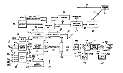
Referring to FIGURE 1, a block diagram of a digital exciter 30 is shown
that generally illustrates the functions implemented by the device. Digital
exciter 30 principally comprises a signal modulator 32 and a digital
quadrature modulator (DQM) 36. The signal modulator is desi~ne~ to sample eithera digital input signal comprising (NRZ) data, or an analog (voice) signal; it
then processes the samples input to it and selectively produces either a complexbaseband frequency modulated (FM) signal, or alternatively, a linear
modulated complex base band signal. Thus, one of the primary advantages of this
digital exciter is its ability to be operated selectively as a linear modulator, capable
forexample, of QAM rnod~ tion of the input signal in a variety of dirre,e,ll
variants, incl~lfling 4QAM and 16QAM. This facility of the digital exciter to
selectively operate in dirre, elll modes is achieved by using a digital
signalprocessor(DSP) for the signal modulator. In the prere"ed embo~imPnt,
two DSPs (Analog DevicesTM, type ADSP 2105), one for signal modlll~tor 32 and
the othercarrying out the functions of DQM 36 and also of an interpolator38,
the purpose of which is licc~lssed below. It should be appale"l to
those of ordinary skill in the art that a single DSP could be used to provide the
functions of signal modulator32, interpolator38, and DQM36 if a device
having sufficient processing speed is available. However, for purposes
of economy, the present prerel l ed embodiment uses two of the devices and
implements the functions of interpolator 38 on the same DSP as used for DQM 36.
Signal modulator 32 is çontrolled by a microprocessor control 40,
which allows an operator to select the mode in which the signal modulator
214~187
WO 94/07302 PCT/US93/078~
--10--
operates, permits setting of various operating parameters, and permits
monitoring of certain conditions during the operation of the signal modulator.
In thep,ere"ed form of the invention, a MotorolaTM, type 68HC11
microcontroller integrated circuit is used for control 40, ~lthollgh many other
5 similardevices can be used in the alternative. Control 40 is programmed to
provide its control functions based upon program steps that are stored in a
memory 42. Although not sel)ala~ely shown, memory 42 comprises both a random
access memory (RAM) for temporary storage of variables and other data, and a
read only memory (ROM) for storing the instructions impl~mented by control 40 to10 carry out its control functions. A bi-directional addressldatabus 44 couples
memory 42 to control 40.
In addition, control40 is col-ne.;Led to a control panel/keyboard46 via
lines 48. The control panel/keyboard allows an operator to enter instructions and
select values for parameters used by control 40 in controlling signal modulator 32. A
display 50 is connected through lines 52 to control 40, providing means for displaying
i,~""dLion to the operator. Lines 54 connect an external interface 56 to control 40,
pel.. iLLh1g a remote video display terminal (VDT) 62 to control signal modulator 32.
For example, VDT 62 allows an operator at location that is geographically
sepa.ate from the location of digital exciter 30 to enter operational parametersused by control 40 and also allows the remote operator to view
operational i--Ço----aLion for the digital exciter through control 40. VDT 62
inr.lndes both a keyboard and display (not separately shown), like
control panel/keyboard 46 and display 50. The VDT at the remote location is linked
to external interface 56 either through a radio link 64, ~cces.cing a radio receiver 58
that is ;"lel-;ol-l-ected to external interface56 through a line60,.or alternatively,
through a telephone line 66, which links the VDT with external interface 56. Details
of external interface 56 and receiver 58 are not shown, since these devices are well
known to those of ordinary skill in the art.
Control 40 is coupled to signal modulator 32 through lines 72, which
connect to latches 70. T.i,t~.hes 70 comprise an 8-bit and a 16-bit latch (not
separately shown) that are coupled to the signal modulator through lines 71. Theprogram run on control 40 is plefe,ably menu driven to f~.ilit~te operator selection
of parameters used to control signal mod~ tor 32. Using the menu presented
on display 50, an operator enters a selection on control paneltkeyboard 46 (or on
the keyboard at the remotely disposed VDT 62). In response to the
operator selection, control40 writes a 16-bit word to the 16-bit latch of
WO 94/07302 2 1 4 ~ 1 8 ~ PCI`/US93/07867
- 1 1 -
latches 70 and sets a flag bit on the 8-bit latch. After the signal modulator DSP
has read the 16-bit word, it resets the flag. Similarly, if the DSP comprising signal
modulator32 is providing status data to control40, it writes a 16-bie word to the
16-bit latch, and sets a di~~ bit on the 8-bit latch, which control 40 resets after it
S has read the 16-bit word. Comm~n~ls from control40 comprise either one or
two 16-bit words, and status data from signal modulator32 typically comprise a
single 16-bit word.
Interaction of signal modulator 32 with control 40 is determined
byprograminstructions loaded into the DSP COlllpliSillg the signal modulator at
10 the time the system is powered up or reset. A boot memory circuit68 stores
the instructions implPm~nt~d by both the DSP comprising signal modulator 32
and the DSP comprising interpolator38 and DQM36. Boot memory circuit68
is coupled to signal modulator 32 through lines 69 and to DQM 36 through
lines 67. The interrupt instructions stored in boot memory circuit 68 that control the
1~ operation of signal modulator 32 are of higher priority than the
background operations it implements, which are related to control and interface
with control 40. Further details concerning the operation of digital exciter 30 and its
interaction with control 40 are di~cl-~ced below.
Input signals to signal modulator 32 are supplied through di~re..l
20 paths, depending upon the type of signal. An analog signal to be modlll~te-l such
as voice, is provided from a source (not shown) over a line 74 that is coupled to
the input of an analog-to-digital converter (ADC) 76. ADC 76 samples the analog
signal supplied on line 74 at a rate of 9765.625 Hz in the p.e~-.ed embodiment,
providing digital values corresponding to the analog signal over a line 78, to
25 signal modlll~tor 32.
An output latch 80 is coupled to signal modulator 32 through data lines 84.
In addition, a write enable line 82 is used for l~tçhing data into output latch 80.
Output latch 80 is used in the context of the present invention only for supplying
a clock (CLK) signal for use in synchronizing a source of digital data when
30 opc-~i--g the digital exciter in a linear modulation mode. The clock signal is
output from output latch 80 on a line 86 and is synchronized with one of the data
bits supplied by signal modulator 32 over lines 84 to output latch 80.
During operation in an asynchronous mode (for FM), the clock signal conveyed on
line 86 is not used. Digital data are input (either synchronously or asynchronously)
3~ asdata bits D0 through D3 on data lines90a through 90d, respectively, to an
input latch 88. During linear modulation of data, the bits provided on lines 90 are
214518~
W O 94/07302 PC~r/US93/078
-12-
read from input latch 88 in synchloni~aLion with the CLK signal and are suppliedover lines 84 to signal mod~ tor 32. During operation in the asynchronous mode,
signal modulator 32 s~mpl~r the input digital data each time that a read (RD)
signal conveyed on a line 96 from signalimodulator 32 to input latch 88 goes low.
~l~hough eight lines 84 couple input latch 88 with signal modulator 32, only four are
used by digital exciter 30 to convey digital input data. In addition, lines 90 convey the
four input bits D0 through D3 to an edge detector circuit 92, which determines
whenthe digital data (in NRZ format) changes logic level, producing an edge
detect interrupt signal that is input to signal mo~l-ll~tor 32 over a line 94.
Edge detector circuit 92 and the interrupt signal it produces are used by signalmodulator 32 for interpolation of the sampled values during operation in
asynchronous FM mode, as explained below.
Signal modulator32 can operate on either two level or four level digital
input data. During asynchronous operation, the DSP comprising signal
modulator 32 does not directly know when a bit begins or ends. Accordingly, signal
modulator 32 uses two interrupt routines, incl~lrling a timer routine and an
external interrupt routine in conjunction with the interrupt signal produced by
edgedetector92. The timer interrupt occurs at an internal frequency of
66-2/3 kHz in the plefe,led embodiment and establishes the rate at which the digital
input signal is processed to produce a pair of complex FSK samples that are
outputfrom the signal modulator. Similarly, when operating in a synchronous
mode, signal modulator 32 also produces a complex output signal having both
amplitude and phase modulation that are conveyed on lines 100 and 102 to the input
of interpolator 38.
Interpolator 38 interpolates the complex signal conveyed on
lines 100/102 from the 66-2/3 kHz sampling rate by a factor of six, yielding a
400 kHz signal. DQM 36 then modulates the sampled signals from the base band to
a first 100 kHz interme~i~te frequency (IF). The quadrature modlll~ted signals
areconll,i"ed and output on a line 108 from DQM 36, for conversion to an
analogsignal by a digital-to-analog converter (DAC) 110. The modulated
outputsignal is then up converted from the lOOkHz frequency by multiplication
with a 89.9 MHz signal produced by a first local oscillator 116. The 89.9MHz
signal is supplied on a line 118 to a multiplier 114 that is coupled to receive
the 100 kHz signal, and the multiplier produces an output frequency of 90 MHz
that is conveyed on a line 120 to a banrip~ filter 122, which elimin~tes
harmonic distortion; the 90 MHz signal is a second IF signal. The second IF signal is
214~1~7
WO 94/07302 -13- PCT/US93/07867
output from b~ntlp~ filter 122 to a multiplier i26 and further up converted to
an output frequency of 900MHz by multiplication with a 810MHz signal
producedby a second local osc~ tQr 128 that is supplied to multiplier 126 over
aline 130. The output signal is conveyed on a line 132 to a power amplifier
5 (not shown).
Operation in FM Mode with Digital Input Data
A functional diagram of signal processor 32 is shown in
FIGURE 2A, illustrating the various operations performed by the signal processorin morl~ ting an NR~ digital input signal during operation in the FM mode.
10 The digital data is provided by a data signal source 138 and as previously described,
issupplied both to input latch 88 and to edge detector circuit 92.
Signal modulator 32 comprises a series of functional blocks that sequentially
process the sampled digital values to produce the complex signal that is provided
to interpolator 38. The data bits that are provided through input latch 88 are read at a
66-2/3 kHz sample rate and input over line 84 to a two or four level mapper
block 140, which maps the bits that it reads to a norm~li7ed level corresponding to the
levels shown in Tables 1 and 2, below.
Table 1 Two Level Data
Data Line 1 Level
+1
O l
Table 2 -- Four Level Data
Data Line 2 Data Line 1 kevel
0 +1
+1/3
0 1 -1/3
O O l
The digital data from data signal source 138 that is sampled by input
latch 88 in response to the read enable signal has values that correspond either to
a binary I or zero. The binary values of the sample data thus relate to the mapping
25 ofthat data tospecific levels. The DSP comprising signal modulator32 works
withvalues thatarenorm~li7ed over the range-l to 1, corresponding to a range
of digital values from -32,767 through 32,767. The two or four level mapper 140
uses a mapped level for the sample data for succes.~ive input samples until the next
21~Sl~7
WO 94/07302 PCI /USg3/0786
--14-
"edge" occurs, co,l~s~,onding to a transition of the input data from one logic level
to a di~,elll logic level, i.e., from a binary 1 to a binary 0 or vice versa. The
mapped levels for the data are supplied through a line 142 to an edge sample
adjusterblock 144. The first mapped sample that occurs imm~ t~ly after a
5 data edge is detected by edge detector circuit 92 is adjusted by edge sample
adjuster block 144 as described below, to reduce jitter that would otherwise occur
in determining the digital value that should be applied to a sample if only level
lllappillg were applied, since the sample is not made at a point n~cPc~rily
synchronous with the transition between binary logic levels of the input data signal.
10 One of the functional parameters that can be selected by an operator is the
inversion of the sample data before mapping occurs. The command to invert or
not invert data is supplied by control 40 over one of the lines 71, as an input to
2/4 level mapper block 140.
If the asynchronous data signal from data signal
15 source 138 were sampled without edge sample adjustm~nt~ the results would be
an inherent jitter of _7.5 microseconds (for 5Z---pl;--p at a 66-2t3 kHz rate).
This jitter occurs because the sampled input data signal would have a zero crossing
at some point midway between the points where the actual samples are taken
on either side of the edge. For use of digital exciter30 in a ~imlllc~ct paging
20 system, amaximum allowable tr~n~mitted data iitter is +0.5 microseconds.
Accordh,gly, it is necess~ry to adjust the digital amplitude of the sample after a
dataedge occurs by an amount proportional to the rli~t~nce of the edge from
the sample just prior to the edge. FIGURES S and 6 illustrate the procedure
for adj~stin~ the edge sample to reduce jitter. In FIGURE 5, a digital
25 NRZ signal having a binary logic level 1 (at reference numeral 250, corresponding
to an NRZ value +l) transitions at an edge 252 to a logic level zero (at
reference numeral 254), corresponding to an NRZ value -1. Subsequently, the
signal transitions at an edge 256 to a logic level 1 (lepresented by a line segm~nt 258).
Corresponding sample values are taken at times indicated in FIGURE 6 by
30 sncc~ive dots appea,il,g along line segmçn~ 250', with an interval tm~X
se~.a,~li"g consecutive samples. All of these samples have a mapping
level cGllt;~,onding to +1. However, a sample 251 taken immedi~tely before
transition252 occurs is adjusted to a value equal to appluxhllately .7 based upon
the time interval t between that sample and transition 252 (or 252'). Similarly,35 a sample255 is ~ssigned an edge a~ sted value of app[oxi"lately -.8. The
amplitude x(i) is determined as follows:
~ WO 94/07302 2 1 4 5 1 8 I PCI/US93/07867
-15-
x(i) = q(i -1) + shift (1)
shi~ = (q(i)-q(i-l))*(t,,~ -t) (2)
In Equation 2 above, q(i) is the norm~li7ed level afler an edge has occurred
and q(i-l) is the norm~li7ed level ofthe input data signal before the edge. Using this
5 technique, a peak jitter rate less than +350 nanoseconds can be obtained, the
pe-ro~-~-ance being d; ..;.~;cl.ed slightly by the time required for the DSP to
execute instructions, which prevents its response to an edge detect signal for a brief
period of time.
To obtain a desired deviation in the inct~nt~neous output frequencies
relative to a carrier frequency, the norm~li7ed samples produced by mapping
and adjusting for edge interpolation are conveyed over a line 146 to a
frequencydeviation adj.lctrnçnt block 148, where the signal is scaled by a
frequency deviation factor. An operator can select the desired frequency
deviation, which control 40 supplies to frequency deviation adj-lctm~nt
block 148 over one of the lines 71. The operator specified frequency deviation
valueis divided by a voltage controlled oscillator (VCO) limit used by a VCO
block 156, to obtain the frequency deviation used, and this value is retained until reset
to a di~el ~nL value.
Following frequency deviation adjl.stmçnt block 148, the signal is
supplied over a line 150 to a delay block 149. Delay block 149 delays the signalon line 150 by a time interval specifically selected to equalize the processing
time incurred during signal modulation of digital input data signals and the
processing time required to signal modulate analog input signals. This
equalization delay ensures that when signal modulator 32 is switched over from
an analog mode to a data mode (or vice versa), that sukst~nti~lly no difference in
the signal modulation processing time is observed. This equalization of the
signal modulation time required for both types of signals is particularly important
in simulcast paging tr~ncmicsions This delay interval can be adjusted by the
operator via command signals that are conveyed from control 40 to delay
block 149 over one of lines 71. The operator can thus select a delay time that
- insure the modulated signal produced by exciter 30 is synchlonized
with corresponding modulated signals tr~n.cmitted from other ~n~ ers in
a sim..lc~ct radio system.
wo 94,o73022 1 4~ 18 7 PCI/US93/078~
-16-
A line 151 conveys the delayed signal to a Bessel low pass filter
(LPF) block 152, which processes the signal by convolving it with a 37 tap
Bessel-type finite impulse response (FIR) filter that meets the ERMES
specifications for a pre-mo~ tion pulse shaping filter. The Bessel LPF block acts
5 as an "anti-splatter" filter to ensure that ~the power spectral density of theL~ ed signal lies within a frequency domain dele,~ ed in accordance with
limits established by the Federal Comm~nic~tions Commission (FCC). Tap values
for the Bessel LPF are illustrated in FIGURE 9. These tap values were determinedbym~t~ ing the frequency response to a ten pole Bessel filter having a
10 cut-offfrequency of 3.9 kHz. FIGURE 10 illustrates the frequency response of
the Bessel LPF block in co",pa~ison to the upper and lower ERMES limits.
The dash-dot line represents the frequency response of the ten pole analog Bessel
filter used to develop the 37 tap values. Bessel LPF block 152 achieves a stop band
~tten-l~tion of app.oxi..~tely 90 dB.
The filtered signal from Bessel LPF block 152 is conveyed on a line 154
to VCO 156 for use in frequency modlll~tin~ the base band carrier conveyed
onlines 100 and 102. A linear transfer function for VCO 156 is illustrated
inFIGlJRE 11. The slope of the linear response for VCO 156 is fma~i Hz/V,
where fmax is the VCO deviation limit, i.e., the largest frequency deviation from
20 the carrier frequency that is possible. The VCO limit value can be changed bythe operator selecting a VCO limit value, which is supplied to VCO 156 over one
of lines71, through latches70 and lines72. The signal input to VCO 156
ismultiplied by the slope of the transfer function, thereby repræsç~ g each
ofthe sampled filtered values as in.~t~nt~neous frequency values. A limiter
25 is employed in VCO 156 to prevent the output from excee-ling the VCO
deviation limit. The complex samples output from VCO 156 are defined by
the following equation:
y(n) = cos~(n) + j sin ~(n) (3)
In Equation 3, the in~t~nt~neous phase of the output, ~(n), is determined
30 inaform that replese--Ls an index to a stored sine lookup table, depending upon
the filtered sampled values that are input. Greater resolution in determining
cosine and sine values is obtained by performing a second order interpolation onthe lookup table values, as explained below. The cosine/sine lookup table is stored
in the internal memory (not separately shown) of the DSP comprising
35 signal modulator 32 and is loaded from boot memory circuit 68 when
WO 94/07302 2 1 ~ 5 1 8 7 PCr/US93/07867
.
--17-
digital exciter 30 is powered up or reset. In a plt:fel-ed embodiment, the lookup
table stores sine values for 128 uniformly spaced angles ranging from zero
to appro~i",~Lely 27~ (127 x 27t/128) around a unit circle. A table index, ~3(n),
is incrennented at each sample instant by ~(n) and by ~of~. The value ~(n)
5 is calculated from the value of the filtered input sample provided to VCO 156 and
the value ~off is c~lc~ ted from a desired frequency offset, which can be çh~nged
by the operator using control 40 to supply the desired value to the VCO.
The following equations define these values:
~(n) = ~(n - I) + ~(n) + ~of~ (4)
~(n) = N x fma~ * input (n)
In the above equations, N is the number of elernents in the sine lookup table (128),
and f5 is the sampling frequency (66-2/3 kHz).
The te~hnique used for determining a sine or cosine value based upon
the sine lookup table and interpolation for angles between the 128 points stored in
15 the table are illustrated in FIGURE 8. The sampled filtered values res~lting
from timed interrupts at the 66-2/3 kHz rate are used to develop pointer ~(n) ina block 262, yielding 16 bits represented by line 264, which are split between
theseven most significant bits (MSBs) inrlic~ted by line264' and the nine
least significant bits (LSBs), represented by line 264". The seven MSBs of the
20 pointer are used for poilllillg to the specific values in the lookup table as indicated
in a block 266, while the nine LSBs are used to carry out a second order
interpolation in a block 270 to improve the resolution with which sine and cosine
aredetermined for angles other than the 128 conl~i"ed within the lookup table.
A line 268 lc;~J,t;se"Ls the value determined from the lookup table based upon
25 the seven MSBs of the pointer, which is applied to the second order
interpolation block. The output of the second order interpolation block is
replese"Ledby a line272 and corresponds to a low-noise interpolated cosine/sine
output.
Second order interpolation block 270 performs two second
30 order interpolations to calculate sine and cosine values, as is well known to those
ofordinary skill in the art. For each interpolation, three table values are usedas supplied over line268 from lookup table block266. Cos ~(n) is determined
inasimilar manner. FIGURE 7 is a simplified illustration of the process
5LEN\b582AP W~
21~51~7
WO 94/07302 -18- PCI'/US93/078
showing howafraction~l value is used to determine the sine of an angle at a
point 260, which is interrne~i~te to lookup table points or angles x(1) and x(2). The
ç~lc~ tion also requires a lookup table value at an angle x(3). Of course,
the simplified illustration in FIGURE 7 ~ep,esenls only a few points (that wouldS be stored in a lookup table) instead of the 128 used in the prerel,ed embodiment.
Itisalso possible to use a table in which fewer points are stored and to use a
third order or higher order interpolation. The output from VCO block 156
comprises theco rl signal conveyed on lines 100/102, which is input to
interpolator 38.
Si~nal Modulator for Linear Modulation of Digital Input Data
Referring now to FIGURE2B, a block diagram for linear modulation as
carried out by signal modulator 32 is illustrated. Data source 138 supplies NRZ
digital data to input latch 88 over lines 90. However, for linear modulation, the data
source is clocked by the clock signal CLK provided by DSP 32 so that the data isprovided to input latch 88 synchronously with the read enable signal provided the
input latch over a line 96. More than one bit of data can be sampled at a time; the
l~n~ ed data rate can therefore exceed 64 kilobits/sec. Furthermore, these digital
input data may comprise digitally compressed voice signals for use in a digital voice
paging system.
In FIGVRE 2B, output latch 80 is omitted to simplify the diagram, since
its sole purpose is to feed through the clock signals from a 2N level
mapperblock 140'. Because the NRZ data is sampled synchronously, edge
detector circuit 92 is not required. In addition, there is no requi,e",c;"~ for
adjustingthe edge to compensate for samples taken at other than zero crossing
transitions of the NRZ data.
The 2N level mapper of FIGURE 2B maps each input data symbol, d(n),
into a corresponding con~t~ tion point on the complex plane. FIGURE 27
shows a mapping for 16 QAM linear modulation, which has four data bits per
data symbol. An impulse of the conctell~tion point for d(n) = I(n) + jQ(n) is fed
intothe pulse ~h~ping filters (which preferably comprise low pass filters) at the
datasymbol rate. The output of the pulse shaping filters is the sampled
continuous time signal I(t) + jQ(t), which is the complex baseband signal. This
signal is then interpolated by interpolator 38 and the interpolated signal is conveyed
to DQM 36, which produces a signal I(t)cos(27~fct) - Q(t)sin(2~fct).
The unfiltered co",plcx base band conveyed on lines 160 and 162 from
the 2N level mapper block are respectively applied to a delay block 163 that
~ WO 94/07302 21~ PCI/US93/07867
-19-
providesa modulation delay interval specified by the operator. The delayed
complexsignal is conveyed over lines 165 and 167 to pulse shaping filters 164
and 166. These pulse shaping filters comprise FIR filters that provide a
desired envelope to the complex output signal conveyed on lines 100/102 to
5 theinterpolator. Lines71 convey signals from control40 to signal modulator32,
enabling operator selection of the digital signal modulation delay and other
parameters in much the same way as described above in connection with the FM
modulator shown in FIGURE 2A.
Details of the Si~nal Modulator for Analo~ (Voice) Input
Turning now to FIGURES 3A and 3B, details of the functional
modulation blocks impl~omented by signal modulator 32 in processing an
analog signal, specifically voice, are illustrated. The samples produced by ADC 76 at
the 9765.625 Hz rate are input on line 78 to a voice processing block 194, whichband pass filters the signal and adjusts its phase. A pre-emphasis filter 198, having
an input connected to the filtered and phase compensated signal from
voice processing block 194 can be selectively applied to provide pre-emphasis ofa voice signal. A line 71b carrying a signal from control 40 via latches 70 controls
a logic switch202 (actually a software flag) that determines whether or
not pre-emphasis filter 198 is applied to the sequential processing of the
filtered and phase compensated signal on line 196. If so, switch 202 selects theoutput signal on aline200 from pre-emphasis filter block 198, passing that
signal to a line 204 as input to an analog frequency deviation block 208.
Otherwise, switch 202 bypasses the pre-emphasis filter block. Frequency deviation
block 208 is used to set the frequency deviation for the voice signal samples by a
value s~lected by the operator and supplied over line 71c.
Re~"ing to FIGURE 3B, the signal output from deviation adjustment
block 208 is input on a line 210 to a sample rate conversion block 214. The
samplerate conversion block uses a combination of a fixed and a linear
interpolation process to raise the effective sampling rate to 66-2/3 kHz. The signal
output from sample rate conversion block 214 on a line 216 at 66-2/3 kHz is input to
a deviation limit adjuctment block or limiter218 having a deviation limit equal or
less than the VCO frequency deviation limit, as determined by an operator
sPlected input conveyed from control 40 through a line 71d. The frequency
limited signal from limiter218 is conveyed on a line220 to a delay block219 and
delayed for a time interval selected by the operator (via a signal conveyed on aline 71g from control 40), so that the modulated signal produced by digital
WO 94~07 ~zL d~ 5 18 ~ PCI'/US93/078
-20-
exciter30 is syncluolu~ed with all of the corresponding tr~ncmissions from otherL~ c~ ers in a ~imlllç~ct radio system. The delayed signal is conveyed through aline 221 to Bessel LPF blQcl~ 152, which performs the functions already
described above, and the output of the Bessel LPF block is conveyed to VCO 156,
which produces the complex output signal.
As shown in FIGURE3B, the complex signal from VCO 156 is
preferably conveyed on lines 226 to a logic switch 228, which is selectively
controlled by the operator using control40. If desired, the operator can
elect toground the output from signal modulator32, cutting off all
tr~n~mi~sions from digital exciter 30. A line 71f conveys the signal that
controls logic switch 228, from control 40 through latches 70. The output from
logic switch 228 is coupled to lines 100/102 as noted above, which are connected to
interpolator 38.
In FIGURE 4, functional details of DQM 36 are shown. A DSP 34 carries
out the functions of DQM 36 and interpolator 38. Accordingly, line 100 is coupled
to an interpolator 38a that provides a 1 to 6 interpolation, increasing the 66-213 I~Iz
sample rate of the in-phase component of the complex signal that is input, to
400 kHz. Similarly, an interpolator 38b receives the guadrature component of
the complex signal on line 102 at 66-2/3 kHz, and provides a 1 to 6
interpolation, yielding an output signal at 400kHz that is conveyed on line 106.Interpolators 38a and 38b comprise 84-tap m--ltib~n~ FIR filters having a
frequency response as shown in FIGURE 12 (the negative portion of
the frequency response having been omitted to simplify the graph). Since
the mllltib~nd FIR filter used for interpolators 38a and 38b is used after five
zeroes are inserted between every two data samples input to the interpolator, for
any interpolation, only 14 taps will have non-zero input samples. Acco, d,"~ ly,the 84-tap filter can be converted into six filters of 14 taps that are applied
in s~cces~ion.
The 400 kHz in-phase and quadrature signals from interpolators 38a
and 38b are respectively input to multipliers 240 and 242. Multiplier 240
multipliesthe 400 kHz in-phase component by cos (27~fcn) and multiplier242
multiplies the quadrature component by -sin(27~fcn). The value fc is the first
IF frequency of 100 kHz. Since the sampling rate is exactly four times
thisIFfrequency, only integer sine and cosine values need to be stored to carry
out the multiplication. Since these values are exact, there is no qu~ ;on
error. The in-phase and quadrature components conveyed on lines 244 and 246
~ W O 94/07302 2i~51~7 PC-r/U593/07867
are then input to an adder 248 to combine the signals, producing the first
IF output signal on line 108. DQM36 thus produces an output modulated
signal at 100 kHz having a time bearing value VIF(t), defined by the
following equation:
v~(t) = vl(t)cos(2~fct)-vQ(t)sin(2~cfct) (7)
DQM36 alternates between interpolations of the two co",ponent of the
complex signal. Up conversion of the 100 kHz interme~ te frequency output from
DQM 36 to obtain a carrier frequency of 900 MHz was explained above.
Operation and Control of the Di~ital Exciter
Digital exciter30 can be selectively operated in one of the plurality of
possible modes, inr.ll~in~ the two level FSK mode, four level FSK mode, flat
analog(voice) mode and pre-emphasized analog (voice) mode. In addition,
the modulation can be selectively set to FM or linear. Control of the
operational mode is available to the operator through control 40 on a menu provided
15 on display 50. The operator can choose between 12 co--~n-lc to change
parameters of operation of the digital exciter. Three of the 12 comm~n-lc affectthe operation of digital exciter 30, regardless of the mode that it is in, and five of the
comm~n~c affect its operation in two level or four level digital data mode. Fourof the co~ n~s affect operation of the digital exciter in either the flat or
pre-emphasized analog mode. Upon hardware reset of the digital exciter,
these co~ and parameters are initi~li7ed to default values.
One of the three co.. ~n~s that affects the exciter's operation, regardless
ofthe mode selecte-i is the col"",and that sets the deviation limit of VCO 156.
Thisdeviation limit specifies the largest possible deviation of the
25 inc~ eous frequency of the output signal from the carrier frequency and can be set
to an integer value between +15 kHz in steps of I Hz. In addition, regardless ofthe mode of operation (~Ithough not shown in all of the figures) logic switch 228 can
be set to stop Ll~n~...;s~;on of the modulated signal by grounding the output
from signal modulator 32. This feature enables an operator to determine the status
30 of digital exciter 30, without tr~n.cmitting a signal, or to temporarily stop the
tr~ncmis.sion of a modulated signal.
Control 40 also enables the operator to offset the carrier frequency for two or
four level data from its default value over a range of+2,048 Hz, in steps of I Hz. The
operator can change the FSK data deviation, which is a deviation of the in.ct~nt~neous
35 output frequencies from the center frequency for the two level or four level data
W094/0730~1 4~187 -2~- ~CI/US93/078
signal modulation, over a range of l 15 kHz, in steps of 1 Hz (up to the VCO limit).
Two comm~nr~c affect ,-apping ofthe logic levels that signal mod~ tor 30 reads from
the NRZ digital input data as shown on Tables 1 and 2, inclu~ling an invert datacor.. and and a non-invert data cor.. -And One of the operator co.. ~nds effects
5 the adj~ctmP-nt of the variable delay in the modulation of the input signal by the digital
exciter.
During operation with an analog input signal, signal modulator 30 can be
cor.. A--~ed to offset the carrier frequency from its default value independent of an
offset chosen when opelaling with digital data. Again, the offset can be any integral
value in the range ~2,048 Hz in steps of 1 Hz. Further, the operator can control the
analog deviation limit, which specifies the largest possible deviation of the
in.ct~nt~neous frequency of the output signal from the carrier frequency. This
deviation limit can be set to any integer value in the range ~15 kHz in steps of I Hz,
subject to the VCO deviation limit. To control the time required for the modulation
15 of an analog input signal, one of the operator con..-.Andc sets the variable delay in the
digital exciter.
Control 40 can also interrogate signal modulator 32 to determine its status,
in~lutling requesting that the signal modulator retum a value indicating its current
mode of operation. In addition, the peak frequency deviation caused by the input20 sampled values can be requested. Further, an input signal detect can be requested by
control 40, which informs the operator whether the digital exciter is receiving an input
signal, based upon whether or not bit transitions are occurring. For operation with
an analog input, signal modulator 30 can also determine and advise control 40
of whether the deviation is eyceeriing 50% of the peak deviation. When
25 edge transitions or peak deviations in excess of 50% are detected by signal
modulator 32, it produces a bit flag indication that control 40 uses to inform the
operator that an input signal is active.
The re~..Ai...l-~ drawing figures, FIGIJRES 13 through 26, are flow
charts that define the operation of digital exciter 30, with respect to its interaction
30 with signal modulator 32. Turning first to FIGURE 13, a reset routine for
signal modulator 32 is illustrated in a flow chart 300. A reset routine impl~rnented
by the digital exciter starts at a step 302, when the device is reset or poweredon. Step 302 causes initi~li7~tion of the control registers that establish
the operation of signal modulator32, and a step 304 initi~li7Ps variables used by
35 it. In a step 306, a delay is provided that is necescAry for syl,cl,lO"i~alion
of signal modulator 32 with DQM 36. This delay is sufficiently long so that
WO ~4/073U2 2 1 4 5 1 ~ 7 PCr/US93/07867
thesignal modulator is assured that DQM36 has completed its
initi~li7~tion operation.
A decision block 308 CO,l" ,ises a loop wherein the signal
modulator determines if a select mode instruction has been received from control 40.
5 If not, the loop continues until the select mode instruction is received, and
then proceeds to a step 310 that clears a read flag from latches 70 and calls a mode
select subroutine that responds to the data transferred from latches 70 to the DSP.
The mode select subroutine enables interrupts 1 and 2. The interrupt 1 routine is
usedif the digital exciter is opelali-lg in an FM mode with two level or four
10 leveldigital input data and is executed when edge detector circuit92 generates
theedge detect interrupt signal. If signal mod~ tor32 is opel~;llg in a flat or
pre-emphasized analog (voice) mode interrupt 1 is a serial port interrupt that is
~Yec~lted whenever a 16bit data word is available to be read at a serial port
receive register (not separately shown) as a sampled input from ADC 76. Interrupt 2
15 is a timer interrupt that occurs at a rate of 66-2/3 kHz and is coupled to respond
to the auto reload timer counter value. The timer counter value is pred~fined for
theDSP, starts at a count of 149, and counts down with each DSP instruction
cycle, generating interrupt 2 when 0 is reached. ~s--ming that signal modulator 32
isoperating in a data input signal mode, the occurrence of interrupt2
20 disables interrupt 1.
A step 318 determines if an edge detect/serial port interrupt has occurred
' (the type of interrupt depending upon the operational mode) and if so,
executes interrupt 1 in a step 320. Since decision step 318 is only reached upon the
occurrence of an edge detect interrupt signal, the logic implemented by the
25 signalmod..l~tor normally proceeds to a decision step312 that determines if the
timer is at 0 and if so, restarts the timer in a step 322. If not, or if the results
fromdecision step318 is negative, the logic proceeds to a step314 that executes
the next instruction of the background program. The background program carries
out instructions responsive to co,.. ~n~ received from control 40. Followingsteps320, 314, or 324, the logic moves to a step316, causing a loop back to
decision step 312 until a reset occurs.
FIGURE 14 illustrates the steps326 for interrupt 1, which is carried out
when digital exciter 30 is operating in a digital data input mode. Pollowing
the occurrence of interrupt 1 in a step 328, a step 330 sets a variable TC (the
timer counter) equal to the current timer value, and a step 332 returns from
the interrupt.
2~45~8~ -
WO 94/07302 PCI'/US93/078~j
-24-
Alternatively, as shown by a flow chart 334 in FIGURE 15, if operating in
an analog mode, interrupt 1 (a serial port interrupt routine) is executed in a
step 336; this interrupt routine occurs at a frequency of 9765.625 Hz, which is
the sampling rate of the analog input signal. In a step 337, an input analog data
5 wordAD(i) is read from ADC 76 and temporarily stored in an internal memory
bufferin signal modulator32. In step338, the sample AD(i) is.voice processed
(filtered) to obtain a filtered sample VP(i). A decision step 339 determines if the
pre-emphasis flag (switch 202 in FIGURE 3A) is set by the background routine, and
if not proceeds to a step 340 that assigns a value PE(i) to VP(i). Conversely, if
10 the operator has selected the pre-emphasis filtering, the logic proceeds to a step 341
that applies the pre-emphasis filter to the rn~gnit~ld~, determining a value PE(i)
based on a convolution of VP(i) with coefficients h2(n), carried out in a infinite
impulce response filter process. Following either steps 340 or 341, a step 343
adjusts PE(i) by a factor delt:. ,..;ned based on the operator selected analog frequency
15 deviation, to determine a value AG(i). The results of this deteination
aretemporarily stored in a step345, and in a step347, the logic returns from
the interrupt.
Turning now to FIGURES 16A and 16B, a flow chart 342 discloses the step
taken in implem~nting interrupt 2 during operation in the digital data signal input
mode (FM). Interrupt 2 starts at a step 344, which is followed by a step 346 in which
interrupt 1 is disabled. A step 348 saves the current timer counter value in a variable
TCS (timer counter saved). In a step 350, the value TC is reset to -1. A step 352
enables interrupt 1. In a decision step 354, the logic determines if the value of TCS is
equal to -1 and if so, proceeds to a step 355 wherein the stored mapped level (based
on previous data samples) for the current mapped level is used. However, if the value
of TCS is between 0 and 149 inclusive, the logic proceeds to a step 356 that reads in
the input bit stream (TxD) from input latch 88 and maps the value to a level used by
the DSP modulation mode that is then active, i.e., FM or linear modulation. A
decision step 358 determines if a four level mapping flag has been set (by
the operator) and if so, proceeds to a step 360 that four level maps the input
bit stream sample (S) to a mapped level SML(i). If ope~Ling with two level
mapping, a step 362 two level maps the input bit stream sample (S) to obtain
the mapped level. Following either step 360 or step 362, a decision step 364
determines if the variable TCS is equal to 148 or 149, and if so, sets TCS equal to 0.
This test is necess~-y because there is a delay of two samples between the time that
an edge detect interrupt is received by signal modulator 32 and the time the
2145187
W0 ~4/07302 PCT/US93/07867
-25-
timervalue is stored in TC. If TCS is equal to 148 or 149, the auto reload
timer counter has been reset prior to the time that the TCS value was stored, and after
the edge detect interrupt signal was generated.
After a step 366 or following a negative response to decision step 364,
5 adecision step368 determines if a timer interrupt signal was generated while
the timer interrupt was disabled, i.e., during the time that the DSP
was execllting instructions and unavailable to process an edge detect interrupt
signal. If so, a step 370 sets TCS to a middle value for the period that the DSPwas disabled. Following a negative response to decision step 368 or after
step 370 is completed, a step 372 determines a shift value for use in a
step 374. Step 374 determines the current mapped level for the input data samplebit stream, interpolated to accommod~te asynchronous sampling of the digital
input data.
A step 376 sets the frequency deviation of the current mapped level as a
function of the frequency deviation variable supplied by the operator, producing a
variable BI(i). At this point, the in-phase complex component of the signal modulator
for the previous timer interrupt is written to DQM36. This value, which was
previously stored in internal data memory within signal modulator 32, is now output
to the DQM in a step 378, the delay in outputting the in-phase value being incurred to
provide a temporal spacing between the in-phase and quadrature components of theoutput signal of at least 25 words, so that the DQM has sufficient time to process
both components.
In a step 380, the signal BI(i) that was stored in the internal data buffer is low
pass filtered by convolving with the cons~rl coefficients of the FIR filter comprising
25 Bessel LPF 152. These coefficients are rep.esel by hl(k).
A step 382 calculates a lookup table inc~ ,enl for the pointer to the
sine lookup table and adds an offset ~off. Next, a step 384 provides for
in~ g the pointer by the value calculated in step 382 to obtain a value for ~(i),
which is in the range 0 to about 128. Seven MSBs of the pointer value represenl
the integer portion and nine bits epresel-~ the fractional portion. A step 386
separates these two portions. The value calculated in step 386 is saved for
the nexttimer interrupt. A step388 causes the timer routine to perform a
second order interpolation, using values of the 128 element sine lookup table.
Starting with elem~ont m-l, the routine determines the quadrature output
component (Q(i)). The pointer is then increm~onted by 32 and the timer
routine pe.ru....s a second order interpolation using the three values of the
Wo 94/073~ 1 4 5 1 8 ~ -26- PCI/US93/078~
128 element lookup table to determine the in-phase component of the complex
signal (I(i)), in a step 390.
A decision step 392 tests the stop l~n~ flag (controlled by the
operator). If set, a step 394 sets I~i~ and Q(i), the complex output signal, to 0.
5 Otherwise, a step 396 stores the current value for the in-phase component of
the complex signal for use during the next timer interrupt. A step 398 writes the
value for the quadrature component (Q(i)) to DQM 36. Thereafter, step 400 returns
from the interrupt.
The steps carried out during linear modulation of a data input
signal are illustrated in FIGURE 28, starting with an interrupt I in a step 600
that occurs at the synchronous input data sample rate. In a step 602, the 2N
level mapper reads N bits (TxD) from input data latch 88 and in a step 606
performsthe 2Nlevel mapping of TxD to obtain I(n) and Q(n), the in-phase
and quadrature components. A step 606 provides for writing a previous pulse
15 shaped value PS(n-1) to DQM 36. The operated sPlected delay for the
linearmodulation is applied to both of the complex signalsI(n) and Q(n) in a
step 608, thereby insuring that the modulated signal produced by exciter 30 will be
synchronized with the modulated signals transmitted from other ~ n~".;llers in a .sim--lc~ct paging system.
A low pass filter acts on the I(n) co,.. ~onent by convolving it with
coefficients h3 in a step 610, yielding the pulse shaped signal IPS(n). Similarly, Q(n)
is low pass filtered in a step 612 by convolving the signal with coefficientc h3, to
determine QPS(n). A step 614 temporarily stores IPS(n) so that it can be written to
the DQM during the next timer interrupt. In a step 616, QPS(n) is written to
DQM 36, and a step 618 then returns from the interrupt.
FIGURES 17A and 17B present the steps for the signal modulator interrupt
routine 2 when the device is operating to modulate an analog (voice) signal. Thetimer interrupt routine 2 starts in a step 402 and proceeds to a step 404 that
resamplesthe 9765.625 Hz sample rate signal AG(i) to 66-2/3 kHz. Samples
from ADC 76 are produced at a 9765.625 Hz rate, and the timer interrupt routine
is based upon samples at a 66-2/3 kHz rate in the prere.led embodiment. A
step 406 sets the analog frequency deviation limit as a function of the
operator s~olected value for this variable (used to produce Dev 2), yielding a signal
value BI(i). The operator selected delay to be applied to the modulation processis~-~cted in a step407 by delaying signal BI. In a step408, the previous in-
phasecomponent I(i-l) is written to the DQM through interpolator38. A low
~ WO 94/07302 2 1 ~ 5 1 ~ 7 PCI/US93/07867
-27-
pass filtering process is applied to the values BI(i) by convolving them with
coefficients hl, producing a low pass filtered signal LPFO(i).
In a step 412, a cosine/sine lookup table incre,.,ent ~(i) is determined as a
function of LPFO(i), a variable VCOL and an offset ~off~ The lookup table pointer is
5 incrçm-onted in a step 414, to determine a new pointer value ~(i). The rç~n~ining
steps 446 through 458 are the same as steps 388 through 400, carried out in
connection with mocl~ tin~ digital input data. Consequently, these steps need not be
again di.ccl-cced
If digital exciter 30 receives a co"--"and to change modes from
10 controller40, a mode change task carried out in a background routine changes a
jump address at the start of the timer interrupt to change to a switch over
timer interrupt routine, which is shown in FIGURE 18. This routine starts at
a step 460, wherein a previous in-phase co."pol1ent I(i-l) is written to DQM 36.Step 460 is necess~ry because the timer interrupt routine operates at a 66-2/3 kHz
15 rate at all times and the signal modulator has no way of stopping the operation of
theDQM. Failure to send in-phase and quadrature components to the DQM as
itexpects would cause signal modulator32 and DQM36 to lose synchrol1iG~Iion
with each other. In switch over interrupt routine 2, provision is made for sçn~ing
the in-phase and quadrature components of the complex signal to the DQM at
20 the required 66-2/3 kHz rate, while the mode select subroutine carries
outvariableinitializations necessary for mode change over. Once these
initializations are completed in the background program, the mode select subroutine
changes the jump address at the start of the timer interrupt to the start address
foroperation ofthe digital exciter in mod-ll~ting either digital or analog (voice)
25 input data.
The final stages of processing are idçntic~l for both analog and digital
data, following a zeroing of the LPF input in a step462 and a delay of the
signal BI for the operator sçlected interval in a step 463. Thus, steps 464
through484are the same as steps380 through400 in FIGURE 16, which were
30 dicc~lcsed above.
A background routine illustrated in FIGURE 19 executes whenever
an interrupt routine is not being ~oxecuted by signal modulator 32. The
background routine is also pre-empted if any interrupt occurs while the
background routine is processing and the routine continuously polls the data
35 available DSP flag bit on the 8-bit input latch 70 until that bit is set. Once the bit
is set, signal processor 32 knows that an instruction from control 40 has been written
-
Wo 94~073~1 45 1 8 7 ~ ~ PCI/US93/078~
to the 16-bit latch, causing the background routine to read the instruction and clear
the data available DSP flag.
There are four tasks that the background routine implements, incl~ding
a software reset, a change in mode of operation, a change in the value of any of5 the parameters ~i~c--~sed above, or a request for the signal modulator to provide
the status of a parameter. The background routine jumps to the start address forthe specific task involved and once it has fini~hed the task, returns to a loop where
it scans the data available DSP flag bit. This procedure is set forth in
FIGURE 19, b~;....i.~g at a start step 486. A decision step 488 determines if the
10 readinstruction flag has been set, and if not, proceeds to step490 that causes
the DSP to loop until the flag bit has been set. Otherwise, the logic proceeds to
a step 492 that provides for reading the instruction from the 16-bit input latch 70.
A step 494 clears the read instruction flag, and a step 496 calls the appropriate
task to be impl~mçnted by the background routine. Thereafter, the routine loops
15 until reset.
In FIGURE 20, a background routine for impl~mtonting a mode change task is
illustrated, b~inni~ at a step 498 that disables interrupt 1. A step 500 then selects
the mode switch over timer routine and selects the timer interrupt jump address as
described above. The a,op,-,~-iate mode select subroutine is called in a step 502.
20 A~er implernenting the mode select subroutine, the logic returns to the main
background routine in a step 504.
Control 40 can set any one of eight parameters in the prert:"~d embodiment,
including the frequency offset of the digital exciter when operating with data input,
the frequency offset of the digital exciter when operating with analog input, the VCO
25 deviation limit, the frequency deviation of the digital exciter when operating with data
input, the frequency deviation of the exciter when operating with an analog input, the
frequency deviation of the digital exciter when operating with an analog input, the
polarity of the digital data mapping, and interruption of the output signal fromVCO 156 (logic switch 228).
FIGURES 21 and 22 respectively cover the background routines for setting
the offsets, deviations, or adjusting frequency deviation, or, the operation to report
the peak frequency deviation in response to a status request. In FIGURE 21, a
step 506 is an entry point to the appr~p,;ate command task routine. A decision
step 508 determines if the read instruction flag has been set (by control 40) and if not,
35 a step 510 causes the logic to loop until the flag is reset. However, if the flag is set, a
step 512 reads the data word from latch 70 and adjusts the selected variables. A
214~1~7
WO 94/07302 PCI/US93/07867
-29-
step 514 then clears the read instruction and set the variables. Thereafter, a step 516
retums to the main background routine.
Similarly, in FIGURE 22, a step 518 inrlic~t~Ps that a peak deviation routine
is to be impkPmPn~ed wherein the signal modulator determines the peak
S frequencydeviation of the sampled input signal. A decision step 520
determineswhether the signal modulator is Op~l~lillg with analog data and if not,
proceeds to a step 528 that returns to the main background routine. However,
if operating in the analog mode, a step 522 c~lc~ tes the peak frequency
deviation ofthe input signal. The peak frequency deviation is then written to the
16-bit latch of latches 70 in a step 524, and an external write data flag in the8-bit latch is set in a step 526. Again, a step 528 subsequently returns the signal
modulator to the main background routine.
Another status request task is detecting whether or not an input signal
is active. FIGURE 23 shows the background routine impleme~t~Pd when a
step 530 calls the modulation detect status request routine. A decision step 532determines if the digital exciter is opel~ g with analog or digital input data. If
with digital data, a step 534 determines if edge transitions are occurring in the data
timer routine, which if so, indicates that modulation is occurring. Conversely, if
opel~tillg with analog data, a step 536 checks the amplitude of the input to
determine if it ever excee(ls a threshold during a predPfine~ period of time, which
only occurs if an input analog signal is present. Subsequently, a step 538 writes
a modulation detect status flag to latches 70 and sets the external write data flag
to the latches in a step 540, before returning to the main background routine ina step 542.
FIG11RES 24 through 26 cover various aspects of the operation of
DQM 36. In FIGURE 24, the steps implemPnted by the reset routine for DQM 36
are illustrated, beg;....;-.p at a step544 that occurs upon reset or power on ofdigital exciter 30. Following such a reset, a step 546 initializes the control
registersand a step 548 initi~li7es variables used by DSP 34. In a step 550,
interrupt 1 is enabled. The DQM then enters a loop waiting for interrupts to
- occur, until reset. In a decision step 552, it determines whether or not a serial
port Ll~ns.,.il interrupt has occurred (interrupt 2), which occurs at a rate of
- 400kHz. If not, the logic continues with a step 560 to loop back to
decision step 552; this loop continues until the device is reset. However, if the
response to decision step 552 is positive, a step 556 executes interrupt 2 and
thereafter proceeds to step 560. At any point, if a read input data interrupt occurs
214~
WO 94/07302 PCI'/US93/078
-30-
(interrupt 1), the occurrence is detected by decision step 554. If so, a step 558
e~cecutes interrupt 1. Otherwise, the response from decision step 554 contin-~es with
step 560, looping until reset.
FIGURE 28 illustrates the steps carried out in implPn entin~: interrupt 1 at a
step 562. During a step 564, the interrupt 1 routine reads in the data word from the
external latch. A decision step 566 determines if this is the first word written to it
from the signal modulator. If so, a step 568 enables interrupt 2. Otherwise, or
after step 568, the logic proceeds to a step 570, returning from the
interrupt. FIGURE26 illustrates the steps implennented during interrupt2 at a
step 572. Following the interrupt, the routine first writes a previous DQM
first intermedi~te frequency output IFO(i-l) to a serial port transmit register so that it
can be sent to DAC 110 in a step 574. In a step 576, a routine is called to
perform the next interpolation. Samples of either the in-phase or quadrature signals
are convolved in a step 578 through one of 12 possible FIR interpolation filters.
Bycycling through the 12 filters, the two operations, including interpolation bya factor of six from 66-2/3 kHz to 400 kHz and modulation to produce the IF
output signal at 100 kHz, are performed simultaneously. The interrupt
routine alternates between filtering in-phase and quadrature components in this
manner and returns from the interrupt at a step 580.
While the p,e~,led embodiment of the invention has been illustrated and
described with respect to the pr~fe.,ed embodiment, it will be appreciated that various
cl-~nges can be made therein without departing from the spirit and scope of the
invention. Accordingly, the scope of the invention is not to be limited by the
description of the prt;fe..ed embodiment, but instead should be determined entirely by
25 reference to the claims that follow.