Note: Descriptions are shown in the official language in which they were submitted.
DEMANDES OU BREVETS VOLUMlNEUX
LA PRESENTE PARTIE DE CETTE DEMANDS OU CE BREVET
COMPREND PLUS D'UN TOME. - _
CECI EST LE TOME DE
NOTE: Pour les tomes additionels, veuiilez contacter !e Bureau canadien des
brevets
~~ ! ~~_~ z Z __
JUMBO APPLlCATiONS/PATENTS
THIS SECTION OF THE APPLICATIONIPATENT CONTAINS MORE
THAN ONE VOLUME
THIS IS VOLUME ~ OF
NOTE: For additional volumes please contact the Canadian Patent Office
CA 02145222 2001-10-22
74078-21
1
MULTISTANDARD VIDEO DECODER AND DECOMPOSITION SYSTEM FOR
PROCESSING ENCODED BIT STREAMS INCLUDING START CODES AND
METHODS RELATING THERETO
BACKGROUND OF THE INVENTION
The present invention is directed to improvements
in methods and apparatus for decompression which operates to
decompress and/or decode a plurality of differently encoded
input signals. The illustrative embodiment chosen for
description hereinafter relates to the decoding of a
plurality of encoded picture standards. More specifically,
this embodiment relates to the decoding of any one of the
well known standards known as JPEG, MPEG and H.261.
A serial pipeline processing system of the present
invention comprises a single two-wire bus used for carrying
unique and specialized interactive interfacing tokens, in
the form of control tokens and data tokens, to a plurality
of adaptive decompression circuits and the like positioned
as a reconfigurable pipeline processor.
Video compression/decompression systems are
generally well-known in the art. However, such systems have
generally been dedicated in design and use to a single
compression standard. They have also suffered from a number
of other inefficiencies and inflexibility in overall system
and subsystem design and data flow management.
Examples of prior art systems and subsystems are
enumerated as follows:
One prior art system is described in United States
Patent No. 5,216,724. The apparatus comprises a plurality
of compute modules, in a preferred embodiment, for a total
of four compute modules coupled in parallel. Each of the
~~ ~ 52z~
2
compute modules has a processor, dual port memory, scratch
pad memory, and an arbitration mechanism. A first bus
couples the compute modules and a host processor. The device
comprises a shared memory which is coupled to the host
processor and to the compute modules with a second bus.
United States Patent No. 4,785,349 discloses a full
motion color digital video signal that is compressed,
formatted for transmission, recorded on compact disc media
and decoded at conventional video frame rates. During
compression, regions of a frame are individually analyzed to
select optimum fill coding methods specific to each region.
Region decoding time estimates are made to optimize
compression thresholds. Region descriptive codes conveying
the size and locations of the regions are grouped together in
a first segment of a data stream. Region fill codes
conveying pixel amplitude indications for the regions are
grouped together according to fill code type and placed in
other segments of the data stream. The data stream segments
are individually variable length coded according to their
respective statistical distributions and formatted to form
data frames. The number of bytes per frame is withered by
the addition of auxiliary data determined by a reverse frame
sequence analysis to provide an average number selected to
minimize pauses of the compact disc during playback, thereby
avoiding unpredictable seek mode latency periods
characteristic of compact discs. A decoder includes a
variable length decoder responsive to statistical information
in the code stream for separately variable length decoding
individual segments of the data stream. Region location data
is derived from region descriptive data and applied with
region fill codes to a plurality of region specific decoders
selected by detection of the fill code type (e. g., relative,
absolute, dyad and DPCM) and decoded region pixels are stored
in a bit map for subsequent display.
2145
3
United States Patent No. 4,922,341 discloses a method
for scene-model-assisted reduction of image data for digital
television signals, whereby a picture signal supplied at time
is to be coded, whereby a predecessor frame from a scene
already coded at time t-1 is present in an image store as a
reference, and whereby the~frame-to-frame information is
composed of an amplification factor, a shift factor, and an
adaptively acquired quad-tree division structure. Upon
initialization of the system, a uniform, prescribed gray
scale value or picture half-tone expressed as a defined
luminance value is written into the image store of a coder at
the transmitter and in the image store of a decoder at the
receiver store, in the same way for all picture elements
(pixels). Both the image store in the coder as well as the
image store in the decoder are each operated with feed back
to themselves in a manner such that the content of the image
store in the coder and decoder can be read out in blocks of
variable size, can be amplified with a factor greater than or
less than 1 of the luminance and can be written back into the
image store with shifted addresses, whereby the blocks of
variable size are organized according to a known quad tree
data structure.
United States Patent No. 5,122,875 discloses an
apparatus for encoding/decoding an HDTV signal. The
apparatus includes a compression circuit responsive to high
definition video source signals for providing hierarchically
layered codewords CW representing compressed video data and
associated codewords T, defining the types of data
represented by the codewords CW. A priority selection
circuit, responsive to the codewords CW and T, parses the
codewords CW into high and low priority codeword sequences
wherein the high and low priority codeword sequences
correspond to compressed video data of relatively greater and
lesser importance to image reproduction respectively. A
zi4~zzz
4
transport processor, responsive to the high and low priority
codeword sequences, forms high and low priority transport
blocks of high and low priority codewords, respectively.
Each transport block includes a header, codewords CW and
error detection check bits. The respective transport blocks
are applied to a forward error check circuit for applying
additional error check data. Thereafter, the high and low
priority data are applied to a modem wherein quadrature
amplitude modulates respective carriers for transmission.
United States Patent No. 5,146,325 discloses a video
decompression system for decompressing compressed image data
wherein odd and even fields of the video signal are
independently compressed in sequences of intraframe and
interframe compression modes and then interleaved for
transmission. The odd and even fields are independently
decompressed. During intervals when valid decompressed
odd/even field data is not available, even/odd field data is
substituted for the unavailable odd/even field data.
Independently decompressing the even and odd fields of data
and substituting the opposite field of data for unavailable
data may be used to advantage to reduce image display latency
during system start-up and channel changes.
United States Patent No. 5,168,356 discloses a video
signal encoding system that includes apparatus for segmenting
encoded video data into transport blocks for signal
transmission. The transport block format enhances signal
recovery at the receiver by virtue of providing header data
from which a receiver can determine re-entry points into the
data stream on the occurrence of a loss or corruption of
transmitted data. The re-entry points are maximized by
providing secondary transport headers embedded within encoded
video data in respective transport blocks.
United States Patent No. 5,168,375 discloses a method
for processing a field of image data samples to provide for
-~ zi4~z2z
one or more of the functions of decimation, interpolation,
and sharpening. This is accomplished by an array transform
processor such as that employed in a JPEG compression system.
Blocks of data samples are transformed by the discrete even
5 cosine transform (DECT) in both the decimation and
interpolation processes, after which the number of frequency
terms is altered. In the case of decimation, the number of
frequency terms is reduced, this being followed by inverse
transformation to produce a reduced-size matrix of sample
points representing the original block of data. In the case
of interpolation, additional frequency components of zero
value are inserted into the array of frequency components
after which inverse transformation produces an enlarged data
sampling set without an increase in spectral bandwidth. In
the case of sharpening, accomplished by a convolution or
filtering operation involving multiplication of transforms of
data and filter kernel in the frequency domain, there is
provided an inverse transformation resulting in a set of
blocks of processed data samples. The blocks are overlapped
followed by a savings of designated samples, and a discarding
of excess samples from regions of overlap. The spatial
representation of the kernel is modified by reduction of the
number of components, for a linear-phase filter, and zero-
padded to equal the number of samples of a data block, this
being followed by forming the discrete odd cosine transform
(DOCT) of the padded kernel matrix.
United States Patent No. 5,175,617 discloses a system
and method for transmitting logmap video images through
telephone line band-limited analog channels. The pixel
organization in the logmap image is designed to match the
sensor geometry of the human eye with a greater concentration
of pixels at the center. The transmitter divides the
frequency band into channels, and assigns one or two pixels
to each channel, for example a 3KHz voice quality telephone
21~522~
6
line is divided into 768 channels spaced about 3.9Hz apart.
Each channel consists of two carrier waves in quadrature, so
each channel can carry two pixels. Some channels are
reserved for special calibration signals enabling the
receiver to detect both the phase and magnitude of the
received signal. If the sensor and pixels are connected
directly to a bank of oscillators and the receiver can
continuously receive each channel, then the receiver need not
be synchronized with the transmitter. An FFT algorithm
implements a fast discrete approximation to the continuous
case in which the receiver synchronizes to the first frame
and then acquires subsequent frames every frame period. The
frame period is relatively low compared with the sampling
period so the receiver is unlikely to lose frame synchrony
once the first frame is detected. An experimental video
telephone transmitted 4 frames per second, applied quadrature
coding to 1440 pixel logmap images and obtained an effective
data transfer rate in excess of 40,000 bits per second.
United States Patent No. 5,185,819 discloses a video
compression system having odd and even fields of video signal
that are independently compressed in sequences of intraframe
and interframe compression modes. The odd and even fields of
independently compressed data are interleaved for
transmission such that the intraframe even field compressed
data occurs midway between successive fields of intraframe
odd field compressed data. The interleaved sequence provides
receivers with twice the number of entry points into the
signal for decoding without increasing the amount of data
transmitted.
United States Patent No. 5,212,742 discloses an
apparatus and method for processing video data for
compression/decompression in real-time. The apparatus
comprises a plurality of compute modules, in a preferred
embodiment, for a total of four compute modules coupled in
r ~.14522~
7
parallel. Each of the compute modules has a processor, dual
port memory, scratch-pad memory, and an arbitration
mechanism. A first bus couples the compute modules and host
processor. Lastly, the device comprises a shared memory
which is coupled to the host processor and to the compute
modules with a second bus. The method handles assigning
portions of the image for each of the processors to operate
upon.
United States Patent No. 5,231,484 discloses a system
and method for implementing an encoder suitable for use with
the proposed ISO/IEC MPEG standards. Included are three
cooperating components or subsystems that operate to
variously adaptively pre-process the incoming digital motion
video sequences, allocate bits to the pictures in a sequence,
and adaptively quantize transform coefficients in different
regions of a picture in a video sequence so as to provide
optimal visual quality given the number of bits allocated to
that picture.
United States Patent No. 5, 267, 334 discloses a method of
removing frame redundancy in a computer system for a sequence
of moving images. The method comprises detecting a first
scene change in the sequence of moving images and generating
a first keyframe containing complete scene information for a
first image. The first keyframe is known, in a preferred
embodiment, as a "forward-facing" keyframe or intraframe, and
it is normally present in CCITT compressed video data. The
process then comprises generating at least one intermediate
compressed frame, the at least one intermediate compressed
frame containing difference information from the first image
for at least one image following the first image in time in
the sequence of moving images. This at least one frame being
known as an interframe. Finally, detecting a second scene
change in the sequence of moving images and generating a
second keyframe containing complete scene information for an
'. 215222
8
image displayed at the time just prior to the second scene
change, known as a "backward-facing" keyframe. The first
keyframe and the at least one intermediate compressed frame
are linked for forward play, and the second keyframe and the
intermediate compressed frames are linked in reverse for
reverse play. The intraframe may also be used for generation
of complete scene information when the images are played in
the forward direction. When this sequence is played in
reverse, the backward-facing keyframe is used for the
generation of complete scene information.
United States Patent No. 5,276,513 discloses a first
circuit apparatus, comprising a given number of prior-art
image-pyramid stages, together with a second circuit
apparatus, comprising the same given number of novel motion-
vector stages, perform cost-effective hierarchical motion
analysis (HMA) in real-time, with minimum system processing
delay and/or employing minimum system processing delay and/or
employing minimum hardware structure. Specifically, the
first and second circuit apparatus, in response to relatively
high-resolution image data from an ongoing input series of
successive given pixel-density image-data frames that occur
at a relatively high frame rate (e.g. , 30 frames per second) ,
derives, after a certain processing-system delay, an ongoing
output series of successive given pixel-density vector-data
frames that occur at the same given frame rate. Each vector-
data frame is indicative of image motion occurring between
each pair of successive image frames.
United States Patent No. 5,283,646 discloses a method
and apparatus for enabling a real-time video encoding system
to accurately deliver the desired number of bits per frame,
while coding the image only once, updates the quantization
step size used to quantize coefficients which describe, for
example, an image to be transmitted over a communications
channel. The data is divided into sectors, each sector
~i~~zzz
9
including a plurality of blocks. The blocks are encoded, for
example, using DCT coding, to generate a sequence of
coefficients for each block. The coefficients can be
quantized, and depending upon the quantization step, the
number of bits required to describe the data will vary
significantly. At the end of the transmission of each sector
of data, the accumulated actual number of bits expended is
compared with the accumulated desired number of bits
expended, for a selected number of sectors associated with
the particular group of data. The system then readjusts the
quantization step size to target a final desired number of
data bits for a plurality of sectors, for example describing
an image. Various methods are described for updating the
quantization step size and determining desired bit
allocations.
The article, Chong, Yong M., A Data-Flow Architecture
for Dictital Image Processing, Wescon Technical Papers: No.
2 Oct./Nov. 1984, discloses a real-time signal processing
system specifically designed for image processing. More
particularly, a token based data-flow architecture is
disclosed wherein the tokens are of a fixed one word width
having a fixed width address field. The system contains a
plurality of identical flow processors connected in a ring
fashion. The tokens contain a data field, a control field
and a tag. The tag field of the token is further broken down
into a processor address ffield and an identifier ffield. The
processor address field is used to direct the tokens to the
correct data-flow processor, and the identifier field is used
to .label the data such that the data-f low processor knows
what to do with the data. In this way, the identifier field
acts as an instruction for the data-flow processor. The
system directs each token to a specific data-flow processor
using a module number (MN). If the MN matches the MN of the
particular stage, then the appropriate operations are
214522
performed upon the data. If unrecognized, the token is
directed to an output data bus.
The article, Kimori, S. et al. An Elastic Pipeline
Mechanism by Self-Timed Circuits, IEEE J. of Solid-State
5 Circuits, Vol. 23, No. 1, February 1988, discloses an elastic
pipeline having self-timed circuits. The asynchronous
pipeline comprises a plurality of pipeline stages. Each of
the pipeline stages consists of a group of input data latches
followed by a combinatorial logic circuit that carries out
10 logic operations specific to the pipeline stages. The data
latches are simultaneously supplied with a triggering signal
generated by a data-transfer control circuit associated with
that stage. The data-transfer control circuits are
interconnected to form a chain through which send and
acknowledge signal lines control a hand-shake mode of data
transfer between the successive pipeline stages.
Furthermore, a decoder is generally provided in each stage to
select operations to be done on the operands in the present
stage. It is also possible to locate the decoder in the
preceding stage in order to pre-decode complex decoding
processing and to alleviate critical path problems in the
logic circuit. The elastic nature of the pipeline eliminates
any centralized control since all the interworkings between
the submodules are determined by a completely localized
decision and, in addition, each submodule can autonomously
perform data buffering and self-timed data-transfer control
at the same time. Finally, to increase the elasticity of the
pipeline, empty stages are interleaved between the occupied
stages in order to ensure reliable data transfer between the
stages.
CA 02145222 2000-OS-10
74078-21
11
Accordingly, those concerned with the design,
development and use of video compression/decompression systems
and related subsystems have long recognized a need for improved
methods and apparatus providing enhanced flexibility,
effeciency and performance. Embodiments of the present
invention may fulfill these needs.
SU1~IARY OF THE INVENTION
In accordance with the present invention, there is
provided a pipelined video decoder and decompression system for
handling a plurality of separately encoded bit streams arranged
as a single serial bit stream of digital bits and having
separately encoded pairs of control codes and corresponding
data carried in the serial bit stream and employing a plurality
of stages interconnected by an interface, said pipelined system
comprising: a start code detector responsive to the single
serial bit stream, for generating control tokens and data
tokens for application to the interface, a respective one of
said tokens including a plurality of data words, each data word
having an extension bit which indicates a presence of
additional words therein, said data words thereby being
unlimited in number; a token decode circuit positioned in
certain of said stages for recognizing certain of said tokens
as control tokens pertinent to that stage and for passing
unrecognized control tokens to a succeeding stage; and a
reconfigurable decode and parser processing means responsive to
a recognized control token for reconfiguring a particular stage
to handle an identified data token.
Also according to the present invention, there is
provided a method of processing video data, said method
comprising: receiving video data having portions encoded in
accordance with respective different video standards, the
plurality of video standards defining corresponding start
CA 02145222 2000-OS-10
74078-21
12
codes; identifying a start code included in the received video
data; and processing the received video data in accordance with
the video standard corresponding to the identified start code.
According to the present invention, there is further
provided a method of processing video data, said method
comprising: receiving a first set of video data encoded in
accordance with a first video standard and having a first start
code defined by the first video standard; determining the video
standard of the first set of video data by identifying the
first start code included in the first set of video data;
processing the first set of video data in accordance with a
first video standard; receiving a second set of video data
encoded in accordance with a second video standard and having a
second start code defined by the second video standard;
determining the video standard of the second set of video data
by identifying the second start code included in the second set
of video data; and processing the second set of video data in
accordance with the second video standard.
According to the present invention there is further
provided a method of processing encoded video data, said method
comprising: receiving video data having portions encoded with
respective different video standards; determining a video
standard from the respective different video standards based on
one of start codes embedded in the video data; generating
tokens demarcating the received video data; and processing the
received video data in accordance with the tokens.
Also according to the invention, there is provided a
method of processing encoded video data at a video data
processing stage, said method comprising: receiving a start
CA 02145222 2000-OS-10
74078-21
12a
identification of one of several video standards of the encoded
video data; configuring the video data processing stage based
on the received start identification; and processing the video
data at the configured video data processing stage in
accordance with the received start identification.
According to the present invention, there is further
provided a method of processing video data, said method
comprising: receiving a first video data code or marker
corresponding to a first video standard; searching video data
for the received video code or marker; receiving a second video
data code or marker corresponding to a second video standard;
and searching video data for the second video data code or
marker.
According to the present invention, there is further
provided, a method of processing video data, the method
comprising: receiving video data; determining a video standard
associated with the video data; generating one or more tokens
for controlling decoding of the received video data by a
decoding pipeline; and decoding the received video data in the
decoding pipeline.
Briefly, and in general terms, embodiments of the
present invention provide a pipeline system having an input
data stream, and a processing stage for receiving the input
data stream the stage including means for recognizing specified
bit stream patterns, whereby said stage facilitates random
access and error recovery. In accordance with embodiments of
the invention, the processing stage may be a start code
detector and the bit stream patterns may include start codes.
Hence, embodiments of the invention provide a search-mode means
for searching differently encoded data streams arranged as a
CA 02145222 2000-OS-10
74078-21
12b
single serial stream of data for allowing random access and
enhanced error recovery.
Examples of embodiments of the present invention will
now be described with reference to the accompanying drawings.
2145222
13
DESCRIPTION OF THE DRAWINGS
Figure. 1 illustrates six cycles of a six-stage pipeline for
different combinations of two internal control signals;
Figures. 2a and 2b illustrate a pipeline in which each stage
includes auxiliary data storage. They also show the manner
in which pipeline stages can "compress" and "expand" in
response to delays in the pipeline;
Figures. 3a(1), 3a(2), 3b(1) and 3b(2) illustrate the control
of data transfer between stages of a preferred embodiment of
a pipeline using a two-wire interface and a multi-phase
clock;
Figure. 4 is a block diagram that illustrates a basic
embodiment of a pipeline stage that incorporates a two-wire
transfer control and also shows two consecutive pipeline
processing stages with the two-wire transfer control;
Figures : 5a and 5b taken together depict one example of a
timing diagram that shows the relationship between timing
signals, input and output data, and internal control signals
used in the pipeline stage as shown in Figure. 4;
Figure. 6 is a block diagram of one example of a pipeline
stage that holds its state under the control of an extension
bit;
Figure. 7 is a block diagram of a pipeline stage' that decodes
stage activation data words;
Figures. 8a and 8b taken together form a block diagram
showing the use of the two-wire transfer control in an
exemplifying "data duplication" pipeline stage;
Figures. 9a and 9b taken together depict one example of a
timing diagram that shows the two-phase clock, the two-wire
transfer control signals and the other internal data and
control signals used in the exemplifying embodiment shown in
Figures. 8a and 8b.
Figure 10 is a block diagram of a reconfigurable processing
stage;
. ~, 2i~5~2~
14
Figure 11 is a block diagram of a spatial decoder;
Figure 12 is a block diagram of a temporal decoder;
Figure 13 is a block diagram of-a video formatter;
Figures 14a-c show various arrangements of memory blocks used
in the present invention:
Figure 14a is a memory map showing a first
arrangement of macroblocks;
Figure 14b is a memory map showing a second
arrangement of macroblocks;
Figure 14c is a memory map showing a further
arrangement of macroblocks;
Figure 15 shows a Venn diagram of possible table selection
values;
Figure 16 shows the variable length of picture data used in
the present invention;
Figure 17 is a block diagram of the temporal decoder
including the prediction filters;
Figure 18 is a pictorial representation of the prediction
filtering process;
Figure 19 shows a generalized representation of the
macroblock structure;
Figure 20 shows a generalized block diagram of a Start Code
Detector;
Figure 21 illustrates examples of start codes in a data
stream;
Figure 22 is a block diagram depicting the relationship
between the flag generator, decode index, header
generator, extra word generator and output latches;
Figure 23 is a block diagram of the Spatial Decoder DRAM
interface;
Figure 24 is a block diagram of a write swing buffer;
Figure 25 is a pictorial diagram illustrating prediction data
offset from the block being processed;
Figure 26 is a pictorial diagram illustrating prediction data
. ~.; 2195z~z
5
offset by (1,1) ;
Figure 27 is a block diagram illustrating the Huffman decoder
and parser state machine of the Spatial Decoder.
Figure 28 is a block diagram illustrating the prediction
filter.
z ~~.-.. 21452 2.2
16
FIGURES
Figure 29 shows a typical decoder system;
Figure 30 shows a JPEG still picture decoder;
Figure 31 shows a JPEG video decoder;
Figure 32 shows a multi-standard video decoder;
Figure 33 shows the start and the end of a token;
Figure 34 shows a token address and data fields;
Figure 35 shows a token on an interface wider than
8 bits;
Figure 36 shows a macroblock structure;
Figure 37 shows a two-wire interface protocol;
Figure 38 shows the location of external two-wire
interfa ces;
Figure 39 shows clock propagation;
Figure 40 shows two-wire interface timing;
Figure 41 shows examples of access structure;
Figure 42 shows a read transfer cycle;
Figure 43 shows an access start timing;
Figure 44 shows an example access with two write
transfe rs;
Figure 45 shows a read transfer cycle;
Figure 46 shows a write transfer cycle;
Figure 47 shows a refresh cycle;
Figure 48 shows a 32 bit data bus and a 256 kbit
deep DRAMs row address);
(9 bit
Figure 49 shows timing parameters for any strobe
signal;
Figure 50 shows timing parameters between any two
strobe signals;
Figure 51 shows timing parameters between a bus
and
a strobe;
Figure 52 shows timing parameters between a bus
and
a strobe;
Figure 53 shows an MPI read timing;
Figure 54 shows an MPI write timing;
Figure 55 shows organization of large integers
in
the mem ory map;
Figure 56 shows a typical decoder clock regime;
Figure 57 shows input clock requirements;
Figure 58 shows the Spatial Decoder;
Figure 59 shows the inputs and outputs of the input
circuit ;
Figure 60 shows the coded port protocol;
Figure 61 shows the start code detector;
Figure 62 shows start codes detected and converted
to Toke ns;
Figure 63 shows the start codes detector passing
Tokens;
Figure 64 shows overlapping MPEG start codes (byte
aligned );
~.., 21952zz
17
Figure 65 shows overlapping MPEG start codes (not
byte aligned);
Figure 66 shows jumping between two video
sequences;
Figure 67 shows a sequence of extra Token
insertion;
Figure 68 shows decoder start-up control;
Figure 69 shows enabled streams queued before the
output;
Figure 70 shows a spatial decoder buffer;
Figure 71 shows a buffer pointer;
Figure 72 shows a video demux;
Figure 73 shows a construction of a picture;
Figure 74 shows a construction of a 4:2:2
macrobTock;
Figure 75 shows a calculating macroblock dimension
from pel ones;
Figure 76 shows spatial decoding;
Figure 77 shows an overview of H.261 inverse
quantization;
Figure 78 shows an overview of JPEG inverse
quantization;
Figure 79 shows an overview of MPEG inverse
quantization;
Figure 80 shows a quantization table memory map;
Figure 81 shows an overview of JPEG baseline
sequential struct ure;
Figure 82 shows a tokenised JPEG picture;
Figure 83 shows a temporal decoder;
Figure 84 shows a picture buffer specification;
Figure 85 shows an MPEG picture sequence (m=3);
Figure 86 shows how "I" pictures are stored and
output;
Figure 87 shows how "P" pictures are formed, stored
and output;
Figure 88 shows how "B" pictures are formed and
output;
Figure 89 shows P picture formation;
Figure 90 shows H.261 prediction formation;
Figure 91 shows an H.261 "sequence";
Figure 92 shows a hierarchy of H.261 syntax;
Figure 93 shows an H.261 picture layer;
Figure 94 shows an H.261 arrangement of groups
of
blocks;
Figure 95 shows an H.261 "slice" layer;
Figure 96 shows an H.261 arrangement of
macroblocks;
Figure 97 shows an H.261 sequence of blocks;
Figure 98 shows an H.261 macroblock layer;
Figure 99 shows an H.261 arrangement of pels in
blocks;
21~5~~2
18
Figure 100 shows a hierarchy of MPEG syntax;
Figure 101 shows an MPEG sequence layer;
Figure 102 shows an MPEG group of pictures layer;
Figure 103 shows an MPEG picture layer;
Figure 104 shows an MPEG "slice" layer;
Figure 105 shows an MPEG sequence of blocks;
Figure 106 shows an MPEG macroblock layer;
Figure 107 shows an "open GOP";
Figure 108 shows examples of access structure;
Figure 109 shows access start timing;
Figure 110 shows a fast page read cycle;
Figure 111 shows a fast page write cycle;
Figure 112 shows a refresh cycle;
Figure 113 shows extracting row and column address
from chip address;
a
Figure 114 shows timing parameters for any strobe
signal;
Figure 115 shows timing parameters between any two
strobe signals;
Figure 116 shows timing parameters between a bus
and
a strobe;
Figure 117 shows timing parameters between a bus
and
a strobe;
Figure 118 shows a Huffman decoder and parser;
Figure 119 shows an H.261 and an MPEG AC Coefficient
Decoding
Flow
Chart;
Figure 120 shows a block diagram for JPEG (AC and
DC) coefficient
decoding;
Figure 121 shows a flow diagram for JPEG (AC and
DC)
coeffic ient decoding;
Figure 122 shows an interface to the Huffman Token
Formatt er;
Figure 123 shows a token formatter block diagram;
Figure 124 shows an H.261 and an MPEG AC Coefficient
Decoding;
Figure 125 shows the interface to the Huffman ALU;
Figure 126 shows the basic structure of the Huffman
ALU;
Figure 127 shows the buffer manager;
Figure 128 shows an imodel and hsppk block diagram;
Figure 129 shows an imex state diagram;
Figure 130 illustrates
the buffer
start-up;
Figure 131 shows a DRAM interface;
Figure 132 shows a write swing buffer;
Figure 133 shows an arithmetic block;
Figure 134 shows an iq block diagram;
Figure 135 shows an iqca state machine;
Figure 136 shows an IDCT 1-D Transform Algorithm;
Figure 137 shows an IDCT 1-D Transform Architecture;
Figure 138 shows a token stream block diagram;
Figure 139 shows a standard block structure;
2~45z~z
19
Figure 140 is a block diagram showing;
microprocessor test access;
Figure 141 shows 1-D Transform Micro-Architecture;
Figure 142 shows a temporal decoder block diagram;
Figure 143 shows the structure of a Two-wire
interface stage;
Figure 144 shows the address generator block
diagram;
Figure 145 shows the block and pixel offsets;
Figure 146 shows multiple prediction filters;
Figure 147 shows a single prediction filter;
Figure 148 shows the 1-D prediction filter;
Figure 149 shows a block of pixels;
Figure 150 shows the structure of the read rudder;
Figure 151 shows the block and pixel offsets;
Figure 152 shows a prediction example;
Figure 153 shows the read cycle;
Figure 154 shows the write cycle;
Figure 155 shows the top-level registers block
diagram with timing references;
Figure 156 shows the control for incrementing
presentation numbers;
Figure 157 shows the buffer manager state machine
(complete);
Figure 158 shows the state machine main loop;
Figure 159 shows the buffer 0 containing an SIF
(22
by 18 macroblocks)
picture;
Figure 160 shows the SIF component 0 with a display
window;
Figure 161 shows an example picture format showing
storage block address;
Figure 162 shows a buffer 0 containing a SIF (22
by
18 macroblocks) picture;
Figure 163 shows an example address calculation;
Figure 164 shows a write address generation state
machine;
Figure 165 shows a slice of the datapath;
Figure 166 shows a two cycle operation of the
datapath;
Figure 167 shows mode 1 filtering;
Figure 168 shows a horizontal up-sampler datapath;
and
Figure 169 shows the structure of the color-space
converter.
<IMG>
<IMG>
21~~222
22
In the ensuing description of the practice of the
invention, the following terms are frequently used and are
generally defined by the following glossary:
GLOSSARY
BLOCK: An 8-row by 8-column matrix of gels, or 64 DCT
coefficients (source, quantized or dequantized).
CHROMINANCE (COMPONENT): A matrix, block or single pel
representing one of the two color difference signals related
to the primary colors in the manner defined in the bit
stream. The symbols used for the color difference signals
are Cr and Cb.
CODED REPRESENTATION: A data element as represented in its
encoded form.
CODED VIDEO BIT STREAM: A coded representation of a series of
one or more pictures as defined in this specification.
CODED ORDER: The order in which the pictures are transmitted
and decoded. This order is not necessarily the same as the
display order.
COMPONENT: A matrix, block or single pel from one of the
three matrices (luminance and two chrominance) that make up
a picture.
COMPRESSION: Reduction in the number of bits used to
represent an item of data.
DECODER: An embodiment of a decoding process.
DECODING (PROCESS) : The process defined in this specification
that reads an input coded bitstream and produces decoded
pictures or audio samples.
DISPLAY ORDER: The order in which the decoded pictures are
displayed. Typically, this is the same order in which they
were presented at the input of the encoder.
ENCODING (PROCESS): A process, not specified in this
specification, that reads a stream of input pictures or audio
samples and produces a valid coded bitstream as defined in
this specification.
21452.2
23
INTRA CODING: Coding of a macroblock or picture that uses
information only from that macroblock or picture.
LUMINANCE (COMPONENT): A matrix, block or single pel
representing a monochrome representation of the signal and
related to the primary colors in the manner defined in the
bit stream. The symbol used for luminance is Y.
MACROBLOCR: The four 8 by 8 blocks of luminance data and the
two ( f or 4 : 2 : 0 chroma format ) f our ( f or 4 : 2 : 2 chroma format
or eight (for 4:4:4 chroma format) corresponding 8 by 8
blocks of chrominance data coming from a 16 by 16 section of
the luminance component of the picture. Macroblock is
sometimes used to refer to the pel data and sometimes to the
coded representation of the pel values and other data
elements defined in the macroblock header of the syntax
defined in this part of this specification. To one of
ordinary skill in the art, the usage is clear from the
context.
MOTION COMPENSATION: The use of motion vectors to improve the
efficiency of the prediction of pel values. The prediction
uses motion vectors to provide offsets into the past and/or
future reference pictures containing previously decoded pel
values that are used to form the prediction error signal.
MOTION VECTOR: A two-dimensional vector used for motion
compensation that provides an offset from the coordinate
position in the current picture to the coordinates in a
reference picture.
NON-INTRA CODING: Coding of a macroblock or picture that uses
information both from itself and from macroblocks and
pictures occurring at other times.
PEL: Picture element.
PICTURE: Source, coded or reconstructed image data. A source
or reconstructed picture consists of three rectangular
matrices of 8-bit numbers representing the luminance and two
chrominance signals. For progressive video, a picture is
2i~~zzz
24
identical to a frame, while for interlaced video, a picture
can refer to a frame, or the top field or the bottom field of
the frame depending on the context.
PREDICTION: The use of a predictor to provide an estimate of
the pel value or data element currently being decoded.
RECONFIGURABLE PROCE88 STAGE (RP8): A stage, which in
response to a recognized token, reconfigures itself to
perform various operations.
SLICE: A series of macroblocks.
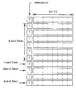
TOKEN: A universal adaptation unit in the form of an
interactive interfacing messenger package for control and/or
data functions.
START CODE8 [8Y8TEM AND VIDEO]: 32-bit codes embedded in a
coded bitstream that are unique. They are used for several
purposes including identifying some of the structures in the
coding syntax.
VARIABLE LENGTH CODING; VLC: A reversible procedure for
coding that assigns shorter code-words to frequent events and
longer code-words to less frequent events.
VIDEO SEQUENCE: A series of one or more pictures.
Detailed Descriptions
2~~5z2z
DESCRIPTION OF THE PREFERRED EMBODIMENT(8)
As an introduction to the most general features used in a
pipeline system which is utilized in the preferred
embodiments of the invention, Fig. 1 is a greatly simplified
5 illustration of six cycles of a six-stage pipeline. (As is
explained in greater detail below, the preferred embodiment
of the pipeline includes several advantageous features not
shown in Fig 1.).
Referring now to the drawings, wherein like reference
10 numerals denote like or corresponding elements throughout the
various figures of the drawings, and more particularly to
Fig. 1, there is shown a block diagram of six cycles in
practice of the present invention. Each row of boxes
illustrates a cycle and each of the different stages are
15 labelled A-F, respectively. Each shaded box indicates that
the corresponding stage holds valid data, i.e., data that is
to be processed in one of the pipeline stages. After
processing (which may involve nothing more than a simple
transfer without manipulation of the data) valid data is
20 transferred out of the pipeline as valid output data.
Note that an actual pipeline application may include more
or fewer than six pipeline stages. As will be appreciated,
the present invention may be used with any number of pipeline
stages. Furthermore, data may be processed in more than one
25 stage and the processing time for different stages can
differ.
In addition to clock and data signals (described below),
the pipeline includes two transfer control signals -- a
"VALID" signal and an "ACCEPT" signal. These signals are
used to control the transfer of data within the pipeline.
The VALID signal, which is illustrated as the upper of the
two .lines connecting neighboring stages, is passed in a
forward or downstream direction from each pipeline stage to
the nearest neighboring device. This device may be another
~l~5zz~
26
pipeline stage or some other system. For example, the last
pipeline stage may pass its data on to subsequent processing
circuitry. The ACCEPT signal, which is illustrated as the
lower of the two lines connecting neighboring stages, passes
in the other direction upstream to a preceding device.
A data pipeline system of the type used in the practice of
the present invention has, in preferred embodiments, one or
more of the following characteristics:
1. The pipeline is "elastic" such that a delay at a
1o particular pipeline stage causes the minimum disturbance
possible to other pipeline stages. Succeeding pipeline
stages are allowed to continue processing and, therefore,
this means that gaps open up in the stream of data
following the delayed stage. Similarly, preceding
pipeline stages may also continue where possible. In this
case, any gaps in the data stream may, wherever possible,
be removed from the stream of data.
2. Control signals that arbitrate the pipeline are
organized so that they only propagate to the nearest
z~ neighboring pipeline stages. In the case of signals
flowing in the same direction as the data flow, this is
the immediately succeeding stage. In the case of signals
flowing in the opposite direction to the data flow, this
is the immediately preceding stage.
3. The data in the pipeline is encoded such that many
different types of data are processed in the pipeline.
This encoding accommodates data packets of variable size
and the size of the packet need not be known in advance.
4. The overhead associated with describing the type of
data is as small as possible.
5. It is possible for each pipeline stage to recognize
only the ~rinimum number of data types that are needed for
its required function. It should, however, still be able
to pass all data types onto the succeeding stage even
27
though it does not recognize them. This enables
communication between non-adjacent pipeline stages.
Although not shown in Fig. 1, there are data lines,
either single lines or several parallel lines, which form a
data bus that also lead into and out of each pipeline stage.
As is explained and illustrated in greater detail below, data
is transferred into, out of, and between the stages of the
pipeline over the data lines.
Note that the first pipeline stage may receive data and
l0 control signals from any form of preceding device. For
example, reception circuitry of a digital image transmission
system, another pipeline, or the like. On the other hand, it
may generate itself, all or part of the data to be processed
in the pipeline. Indeed, as is explained below, a "stage"
15 may contain arbitrary processing circuitry, including none at
all (for simple passing of data) or entire systems (for
example, another pipeline or even multiple systems or
pipelines), and it may generate, change, and delete data as
desired.
20 when a pipeline stage contains valid data that is to be
transferred down the pipeline, the VALID signal, which
indicates data validity, need not be transferred further than
to the immediately subsequent pipeline stage. A two-wire
interface is, therefore, included between every pair of
25 pipeline stages in the system. This includes a two-wire
interface between a preceding device and the first stage, and
between a subsequent device and the last stage, if such other
devices are included and data is to be transferred between
them and the pipeline.
~0 Each of the signals, ACCEPT and VALID, has a HIGH and a
LOW value. These values are abbreviated as "H" and "L",
respectively. The most common applications of the pipeline,
in practicing the invention, will typically be digital. In
such digital implementations, the HIGH value may, zor
. ~..., zl~~z.zz.
2 8~
example, be a logical "1" and the LOw value may be a logical
"O". The system is not restricted to digital
implementations, however, and in analog implementations, the
HIGH value may be a voltage or other similar quantity above
(or below) a set threshold, with the LOW value being
indicated by the corresponding signal being below (or above)
the same or some other threshold. For digital applications,
the present invention may be implemented using any known
technology, such as CMOS, bipolar etc.
It is not necessary to use a distinct storage device and
wires to provide for storage of VALID signals. This is true
even in a digital embodiment. All that is required is that
the indication of "validity" of the data be stored along with
the data. By way of example only, in digital television
pictures that are represented by digital values, as specified
in the international standard CCIR 601, certain specific
values are not allowed. In this system, eight-bit binary
numbers are used to represent samples of the picture and the
values zero and 255 may not be used.
2o If such a picture were to be processed in a pipeline built
in the practice of the present invention, then one of these
values (zero, for example) could be used to indicate that the
data in a specific stage in the pipeline is not valid.
Accordingly, any non-zero data would be deemed to be valid.
In this example, there is no specific latch that can be
identified and said to be storing the "validness" of the
associated data. Nonetheless, the validity of the data is
stored along with the data.
As shown in Fig. 1, the state of the VALID signal into
each stage is indicated as an "H" or an "L" on an upper,
right-pointed arrow. Therefore, the VALID signal from Stage
A into Stage B is LOw, and the VALID signal from Stage D in'o
Stage E is HIGH. The state of the ACCEPT signal into each'
stage is indicated as an "H" or an "L" on a lower, ~ef=-
. ~:, 2~~:~zzz.
29
pointing arrow. Hence, the ACCEPT signal from Stage E into
Stage D is HIGH, whereas the ACCEPT signal from the device
connected downstream of the pipeline into Stage F is LOW.
Data is transferred from one stage to another during a
cycle (explained below) whenever the ACCEPT signal of the
downstream stage into its upstream neighbor is HIGH. If the
ACCEPT signal is LOW between two stages, then data is not
transferred between these stages.
Referring again to Fig. 1, if a box is shaded, the
to corresponding pipeline stage is assumed, by way of example,
to contain valid output data. Likewise, the VALID signal
which is passed from that stage to the following stage is
HIGH. Fig. 1 illustrates the pipeline when stages B, D, and
E contain valid data. Stages A, C, and F do not contain
valid data. At the beginning, the VALID signal into pipeline
stage A is HIGH, meaning that the data on the transmission
line into the pipeline is valid.
Also at this time, the ACCEPT signal into pipeline stage
F is LOW, so that no data, whether valid or not, is
2o transferred out of Stage F. Note that both valid and invalid
data is transferred between pipeline stages. Invalid data,
which is data not worth saving, may be written over, thereby,
eliminating it from the.pipeline. However, valid data must
. not be written over since it is data that must be saved for
processing or use in a downstream device e.g., a pipeline
stage, a device or a system connected to the pipeline that
receives data from the pipeline.
In the pipeline illustrated in Fig. 1, Stage E contains
valid data D1, Stage D contains valid data D2, Stage B
G contains valid data D3, and a device (not shown) connected to
the pipeline upstream contains data D4 that is to be
transferred into and processed in the pipeline. Stages B,
and E, in addition to the upstream device, contain valid data
and, therefore, the VALID signal from these stages or devices
2~.45~2~
. ~:
into their respective following devices is HIGH. The VALID
signal from the Stages A, C and F is, however, LOW since
these stages do not contain valid data.
Assume now that the device connected downstream from the
5 pipeline is not ready to accept data from the pipeline. The
device signals this by setting the corresponding ACCEPT
signal LOW into Stage F. Stage F itself, however, does not
contain valid data and is, therefore, able to accept data
from the preceding Stage E. Hence, the ACCEPT signal from
to Stage F into Stage E is set HIGH.
Similarly, Stage E contains valid data and Stage F is
ready to accept this data. Hence, Stage E can accept new
data as long as the valid data D1 is first transferred to
Stage F. In other words, although Stage F cannot transfer
15 data downstream, all the other stages can do so without any
valid data being overwritten or lost. At the end of Cycle 1,
data can, therefore, be "shifted" one step to the right.
:his condition is shown in Cycle 2.
In the illustrated example, the downstream device is still
2G not ready to accept new data in Cycle 2 and, therefore, the
ACCEPT signal into Stage F is still LOw. Stage F cannot,
therefore, accept new data since doing so would cause valid
data D1 to be overwritten and lost. The ACCEPT signal from
Stage F into Stage E, therefore, goes LOW, as does the ACCEPT
25 signal from Stage E into Stage D since Stage E also contains
valid data D2. All of the Stages A-D, however, are able to
accept new data (either because they do not contain valid
data or because they are able to shift their valid data
downstream and accept new data) and they signal this
condition to their immediately preceding neighbors by setting
their corresponding ACCEPT signals HIGH.
The state of the pipelines after Cycle 2 is illustrated in
Fig. 1 for the row labelled Cycle 3. By way of example, it
is assumed that the downstream device is still not ready tc
. ~..., 2145 2'~2
31
accept new data from Stage F (the ACCEPT signal into Stage F
is LOW). Stages E and F, therefore, are still "blocked", but
in Cycle 3, Stage D has received the valid data D3, which has
overwritten the invalid data that was previously in this
stage. Since Stage D cannot pass on data D3 in Cycle 3, it
cannot accept new data and, therefore, sets the ACCEPT signal
into Stage C LOW. However, stages A-C are ready to accept
new data and signal this by setting their corresponding
ACCEPT signals HIGH. Note that data D4 has been shifted from
Stage A to Stage B.
Assume now that the downstream device becomes ready to
' accept new data in Cycle 4. It signals this to the pipeline
by setting the ACCEPT signal into Stage F HIGH. Although
Stages C-F contain valid data, they can now shift the data
downstream and are, thus, able to accept new data. Since
each stage is therefore able to shift data one step
downstream, they set their respective ACCEPT signals out
HIGH.
As long as the ACCEPT signal into the final pipeline stage
(in this example, Stage F) is HIGH, the pipeline shown in
Fig. 1 acts as a rigid pipeline and simply shifts data one
step downstream on each cycle. Accordingly, in Cycle 5, data
D1, which was contained in Stage F in Cycle 4, is shifted out
of the pipeline to the subsequent device, and all other data
is shifted one step downstream.
Assume now, that the ACCEPT signal into Stage F goes LOW
in Cycle 5. Once again, this means that Stages D-F are not
able to accept new data, and the ACCEPT signals out of these
stages into their immediately preceding neighbors go LOh.
~u Hence, the data D2, D3 and D4 cannot shift downstrea:~,
ho~,~~ever, the data D5 can. The corresponding state of the
pipeline after Cycle 5 is, thus, shown in Fig. 1 as Cycle 6.
The ability of the pipeline, in accordance with the
preferred embodiments of the present invention, to "fill up"
~, 214~2~~
32
empty processing stages is highly advantageous since the
processing stages in the pipeline thereby become decouple
from one another. In other words, even though a pipeline
stage may not be ready to accept data, the entire pipeline
does not have to stop and wait for the delayed stage.
Rather, when one stage is unable to accept valid data it
simply forms a temporary "wall" in the pipeline.
Nonetheless, stages downstream of the "wall" can continue to
advance valid data even to circuitry connected to the
l0 pipeline, and stages to the left of the "wall" can still
accept and transfer valid data downstream. Even when several
pipeline stages temporarily cannot accept new data, other
stages can continue to operate normally. In particular, the
pipeline can continue to accept data into its initial stage
~5 A as long as stage A does not already contain valid data that
cannot be advanced due to the next stage not being ready to
accept new data. As this example illustrates, data can be
transferred into the pipeline and between stages even when
cne or more processing stages is blocked.
~0 In the embodiment shown in Fig. 1, it is assumed that the
various pipeline stages do not store the ACCEPT signals they
receive from their immediately following neighbors. Instead,
whenever the ACCEPT signal into a downstream stage goes LOW,
this LOw signal is propagated upstream as far as the nearest
25 pipeline stage that does not contain valid data. For
example, referring to Fig. 1, it was assumed that the ACCEPT
signal into Stage F goes LOW in Cycle 1. In Cycle 2, the LCW
signal propagates from Stage F back to Stage D.
In Cycle 3, when the data D3 is latched into Stage D, the
ACCEPT signal propagates upstream four stages to Stage C.
wi~,en the ACCEPT signal into Stage F goes HIGH in Cycle 4, it
must propagate upstream all the way to Stage C. In other
words, the change in the ACCEPT signal must propagate back
four stages. It is not necessary, however, in the embodiment
21~5~2~
33
i l lustrated in Fig . 1, f or the ACCEPT s igna 1 to propagate a 11
the way back to the beginning of the pipeline if there is
some intermediate stage that is able to accept new data.
In the embodiment illustrated in Fig. 1, each pipeline
stage will still need separate input and output data latches
to allow data to be transferred between stages without
unintended overwriting. Also, although the pipeline
illustrated in Fig. 1 is able to "compress" when downstream
pipeline stages are blocked, i.e., they cannot pass on the
1G data they contain, the pipeline does not "expand" to provide
stages that contain no valid data between stages that do
contain valid data. Rather, the ability to compress depends
on there being cycles during which no valid data is presented
to the first pipeline stage.
In Cycle 4, for example, if the ACCEPT signal into Stage
F remained LOW and valid data filled pipeline stages A and B,
as long as valid data continued to be presented to Stage A
the pipeline would not be able to compress any further and
valid input data could be lost. Nonetheless, the pipeline
2C illustrated in Fig. 1 reduces the risk of data loss since it
is able to compress as long as there is a pipeline stage that
does not contain valid data.
Fig. 2 illustrates another embodiment of the pipeline that
can both compress and expand in a logical manner and which
includes circuitry that limits propagation of the ACCEPT
signal to the nearest preceding stage. Although tfi~e
circuitry for implementing this embodiment is explained and
illustrated in greater detail below, Fig. 2 serves to
illustrate the principle by which it operates.
3~ For ease of comparison only, the input data and ACCEPT
signals into the pipeline embodiment shown in Fig. 2 are the
same as in the pipeline embodiment shown in Fig. 1.
Accordingly, stages E, D and B contain valid data D1, v2 and
D3, respectively. The ACCEPT signal into Stage F is LOt~; and
. ~., ~1~5~2~
34
data D4 is presented to the beginning pipeline Stage A. In
Fig. 2, three lines are shown connecting each neighboring
pair of pipeline stages. The uppermost line, which may be a
bus, is a data line. The middle line is the line over which
the VALID signal is transferred, while the bottom line is the
line over which the ACCEPT signal is transferred. Also, as
before, the ACCEPT signal into Stage F remains LOW except in
Cycle 4. Furthermore, additional data D5 is presented to the
pipeline in Cycle 4.
to In Fig. 2, each pipeline stage is represented as a block
divided into two halves to illustrate that each stage in this
embodiment of the pipeline includes primary and secondary
data storage elements. In Fig. 2, the primary data storage
is shown as the right half of each stage. However, it will
be appreciated that this delineation is for the purpose of
illustration only and is not intended as a limitation.
As Fig. 2 illustrates, as long as the ACCEPT signal into
a stage is HIGH, data is transferred from the primary storage
elements of the stage to the secondary storage elements of
the Following stage during any given cycle. Accordingly,
although the ACCEPT signal into Stage F is LOW, the ACCEPT
signal into all other stages is HIGH so that the data D1, D2
and D3 is shifted forward one stage in Cycle 2 and the data
D4 is shifted into the first Stage A.
~5 t'p to this point, the pipeline embodiment shown in Fig. 2
acts in a manner similar to the pipeline embodiment shown in
Fig. 1. The ACCEPT signal from Stage F into Stage E,
however, is HIGH even though the ACCEPT signal into Stage F
is LOW. As is explained below, because of the secondary
J;: storage elements, it is not necessary for the LOW ACCEPT
signal to propagate upstream beyond Stage F. Moreover, by
leaving the ACCEPT signal into Stage E HIGH, Stage F signals
that it is ready to accept new data. Since Stage F is nct
able to transfer the data D1 in its primary storage ele~:~ents
~.., 21~5~~~
downstream (the ACCEPT signal into Stage F is LOW) in Cycle
3, Stage E must, therefore, transfer the data D2 into the
secondary storage elements of Stage F. Since both the
primary and the secondary storage elements of Stage F now
5 contain valid data that cannot be passed on, the ACCEPT
signal from Stage F into Stage E is set LOW. Accordingly,
this represents a propagation of the LOW ACCEPT signal back
only one stage relative to Cycle 2, whereas this ACCEPT
signal had to be propagated back all the way to Stage C in
10 the embodiment shown in Fig. 1.
Since Stages A-E are able to pass on their data, the
ACCEPT signals from the stages into their immediately
preceding neighbors are set HIGH. Consequently, the data D3
and D4 are shifted one stage to the right so that, in Cycle
15 4, they are loaded into the primary data storage elements of
Stage E and Stage C, respectively. Although Stage E now
contains valid data D3 in its primary storage elements, its
secondary storage elements can still be used to store other
data without risk of overwriting any valid data.
Assume now, as before, that the ACCEPT signal into Stage
F becomes HIGH in Cycle 4. This indicates that the
downstream device to which the pipeline passes data is ready
to accept data from the pipeline. Stage F, however, has set
its ACCEPT signal LOW and, thus, indicates to Stage E that
25 Stage F is not prepared to accept new data. Observe that the
ACCEPT signals for each cycle indicate what will "happen" in
the next cycle, that is, whether data will be passed on
(ACCEPT HIGH) or whether data must remain in place (ACCEPT
LOW) . Therefore, from Cycle 4 to Cycle 5, the data D1 is
3;: passed from Stage F to the following device, the data D2 is
shifted from secondary to primary storage in Stage F, but the
data D3 in Stage E is not transferred to Stage F. The data
D4 and D5 can be transferred into the following pipeline
stages as normal since the following stages have their ACCEPT
. ~,.., 21~~2~2.
36
signals HIGH.
Comparing the state of the pipeline in Cycle 4 and Cycle
5, it can be seen that the provision of secondary storage
elements, enables the pipeline embodiment shown in Fig. 2 to
expand, that is, to free up data storage elements into which
valid data can be advanced. For example, in Cycle 4, the
data blocks D1, D2 and D3 form a "solid wall" since their
data cannot be transferred until the ACCEPT signal into Stage
F goes HIGH. Once this signal does become HIGH, however,
to data D1 is shifted out of the pipeline, data D2 is shifted
into the primary storage elements of Stage F, and the
secondary storage elements of Stage F become free to accept
new data if the following device is not able to receive the
data D2 and the pipeline must once again "compress." This is
shown in Cycle 6, for which the data D3 has been shifted into
the secondary storage elements of Stage F and the data D4 has
been passed on from Stage D to Stage E as normal.
Figs. 3a(1), 3a(2), 3b(1) and 3b(2) (which are referred to
collectively as Fig. 3) illustrate generally a preferred
embodiment of the pipeline. This preferred embodiment
implements the structure shown in Fig. 2 using a two-phase,
non-overlapping clock with phases o0 and e1. Although a two
phase clock is preferred, it will be appreciated that it is
also possible to drive the various embodiments of the
invention using a clock with more than two phases.
As shown in Fig. 3, each pipeline stage is represented as
having two separate boxes which illustrate the primary and
secondary storage elements. Also, although the VALID signal
and the data lines connect the various pipeline stages as
before, for ease of illustration, only the ACCEPT signal is
s:~own in Fig. 3. A change of state during a clock phase of
certain of the ACCEPT signals is indicated in Fig. 3 using an
upward-pointing arrow for changes from LOW to HIGH.
Similar 1y, a downward-pointing arrow for changes from HIGH to
214522.
37
LOW. Transfer of data from one storage element to another is
indicated by a large open arrow. It is assumed that the
VALID signal out of the primary or secondary storage elements
of any given stage is HIGH whenever the storage elements
contain valid data.
In Fig. 3 , each cycle is shown as consisting of a full
period of the non-overlapping clock phases ~0 and o1. As is
explained in greater detail below, data is transferred from
the secondary storage elements (shown as the left box in each
to stage) to the primary storage elements (shown as the right
box in each stage) during clock cycle o1, whereas data is
transferred from the primary storage elements of one stage to
the secondary storage elements of the following stage during
the clock cycle o0. Fig. 3 also illustrates that the primary
and secondary storage elements in each stage are further
connected via an internal acceptance line to pass an ACCEPT
signal in the same manner that the ACCEPT signal is passed
from stage to stage. In this way, the secondary storage
element will know when it can pass its date to the primary
storage element.
Fig. 3 shows the of phase of Cycle 1, in which data D1, D2
and D3, which were previously shifted into the secondary
storage elements of Stages E, D and B, respectively, are
_ shifted into the primary storage elements of the respective
2~ stage. During the of phase of Cycle 1, the pipeline,
therefore, assumes the same configuration as is shown as
Cycle 1 of Fig. 2. As before, the ACCEPT signal into Stage
F is assumed to be LOW. As Fig. 3 illustrates, however, this
means that the ACCEPT signal into the primary storage element
of Stage F is LOW, but since this storage element does not
contain valid data, it sets the ACCEPT signal into its
secondary storage element HIGH.
The ACCEPT signal from the secondary storage elements of
Stage F into the primary storage elements of Stage E is also
21452~~
38
set HIGH since the secondary storage elements of Stage F do
not contain valid data. As before, since the primary storage
elements of Stage F are able to accept data, data in all the
upstream primary and secondary storage elements can be
shifted downstream without any valid data being overwritten.
The shift of data from one stage to the next takes place
during the next 00 phase in Cycle 2. For example, the valid
data D1 contained in the primary storage element of Stage E
is shifted into the secondary storage element of Stage F, the
l0 data D4 is shifted into the pipeline, that is, into the
secondary storage element of Stage A, and so forth.
The primary storage element of Stage F still does not
contain valid data during the a0 phase in Cycle 2 and,
therefore, the ACCEPT signal from the primary storage
1~ elements into the secondary storage elements of Stage F
remains HIGH. During the 01 phase in Cycle 2, data can
therefore be shifted yet another step to the right, i.e.,
from the secondary to the primary storage elements within
each stage.
2o However, once valid data is loaded into the primary
storage elements of Stage F, if the ACCEPT into Stage F from
the downstream device is still LOW, it is not possible to
shift data out of the secondary storage element of Stage F
without overwriting and destroying the valid data D1. The
25 ACCEPT signal from the primary storage elements into the
secondary storage elements of Stage F therefore goes LOw.
Data D2, however, can still be shifted into the secondary
storage of Stage F since it did not contain valid data and
its ACCEPT signal out was HIGH.
'~ During the of phase of Cycle 3, it is not possible to
shift data D2 into the primary storage elements of Stage
although data can be shifted within all the previous stages.
Once valid data is loaded into the secondary storage elements
of Stage F, however, Stage F is not able to pass on this
~' 21~522~
39
data. It signals this event setting its ACCEPT signal out
LOW.
Assuming that the ACCEPT signal into Stage F remains LOW,
data upstream of Stage F can continue to be shifted between
S stages and within stages on the respective clock phases until
the next valid data block D3 reaches the primary storage
elements of Stage E. As illustrated, this condition is
reached during the Q1 phase of Cycle 4.
During the o0 phase of Cycle 5, data D3 has been loaded
to into the primary storage element of Stage E. Since this data
cannot be shifted further, the ACCEPT signal out of the
primary storage elements of Stage E is set LOW. Upstream
data can be shifted as normal.
Assume now, as in Cycle 5 of Fig. 2, that the device
15 connected downstream of the pipeline is able to accept
pipeline data. It signals this event by setting the ACCEPT
signal into pipeline Stage F HIGH during the al phase of
Cycle 4. The primary storage elements of Stage F can now
shift data to the right and they are also able to accept new
data. Hence, the data D1 was shifted out during the of phase
of Cycle 5 so that the primary storage elements of Stage F no
longer contain data that must be saved. During the e1 phase
of Cycle 5, the data D2.is, therefore, shifted within Stage
F from the secondary storage elements to the primary storage
25 elements. The secondary storage elements of Stage F are also
able to accept new data and signal this by setting the ACCEPT
signal into the primary storage elements of Stage E HIGH.
During transfer of data within a stage, that is, from its
secondary to its primary storage elements, both sets of
storage elements will contain the same data, but the data in
the secondary storage elements can be overwritten with no
data loss since this data will also be held in the primary
storage elements: The same holds true for data transfer from
the primary storage elements of one stage into the seccndary
2 ~ ~ 5'~ 2 ~.
storage elements of a subsequent stage.
Assume now, that the ACCEPT signal into the primary
storage elements of Stage F goes LOW during the Q1 phase in
Cycle 5. This means that Stage F is not able to transfer the
5 data D2 out of the pipeline. Stage F, consequently, sets the
ACCEPT signal from its primary to its secondary storage
elements LOW to prevent overwriting of the valid data D2.
The data D2 stored in the secondary storage elements of Stage
F, however, can be overwritten without loss, and the data D3,
1~ is therefore, transferred into the secondary storage elements
of Stage F during the a0 phase of Cycle 6. Data D4 and D5
can be shifted downstream as normal. Once valid data D3 is
stored in Stage F along with data D2, as long as the ACCEPT
signal into the primary storage elements of Stage F is LOW,
neither of the secondary storage elements can accept new
data, and it signals this by setting the ACCEPT signal into
Stage E LOW.
When the ACCEPT signal into the pipeline from the
downstream device changes from LOW to HIGH or vice versa,
20 this change does not have to propagate upstream within the
pipeline further than to the immediately preceding storage
elements (within the same stage or within the preceding
pipeline stage). Rather, this change propagates upstream
within the pipeline one storage element block per clock
2~ phase.
As this example illustrates, the concept of a "stage" in
the pipeline structure illustrated in Fig. 3 is to some
extent a matter of perception. Since data is transferred
within a stage (from the secondary to the primary storage
eler~,ents) as it is between stages (from the primary storage
eleø;~ents of the upstream stage into the secondary storage
elements of the neighboring downstream stage) , one could just
as well consider a stage to consist of "primary" storage
elements followed by "secondary storage elements" instead ~,f
~,.. 2~.4~22~
41
as illustrated in Fig. 3. The concept of "primary" and
"secondary" storage elements is, therefore, mostly a question
of labeling. In Fig. 3, the "primary" storage elements can
also be referred to as "output" storage elements, since they
are the elements from which data is transferred out of a
stage into a following stage or device, and the "secondary"
storage elements could be "input" storage elements for the
same stage.
In explaining the aforementioned embodiments, as shown in
?0 Figs. 1-3, only the transfer of data under the control of the
ACCEPT and VALID signals has been mentioned. It is to be
further understood that each pipeline stage may also process
the data it has received arbitrarily before passing it
between its internal storage elements or before passing it to
the following pipeline stage. Therefore, referring once
again to Fig. 3, a pipeline stage can, therefore, be defined
as the portion of the pipeline that contains input and output
storage elements and that arbitrarily processes data stored
in its storage elements.
Furthermore, the "device" downstream from the pipeline
Stage F, need not be some other type of hardware structure,
but rather it can be another section of the same or part of
another pipeline. As illustrated below, a pipeline stage can
set its ACCEPT signal LOw not only when all of the downstream
storage elements are filled with valid data, but also when a
stage requires more than one clock phase to finish processing
its data. This also can occur when it creates valid data in
one or both of its storage elements. In other words, it is
not necessary for a stage simply to pass on the ACCEPT signal
based on whether or not the immediately downstream storage
elements contains valid data that cannot be passed on.
Rather, the ACCEPT signal itself may also be altered within
the stage or, by circuitry external to the stage, in order to
ccntrol the passage of data between adjacent storage
~,:, 21 ~ ~ ~'~ ~
42
elements. The VALID signal may also be processed in an
analogous manner.
A great advantage of the two-wire interface (one wire for
each of the VALID and ACCEPT signals) is its ability to
S control the pipeline without the control signals needing to
propagate back up the pipeline all the way to its beginning
stage. Referring once again to Fig. 1, Cycle 3, for example,
although stage F "tells" stage E that it cannot accept data,
and stage E tells stage D, and stage D tells stage C.
Indeed, if there had been more stages containing valid data,
then this signal would have propagated back even further
along the pipeline. In the embodiment shown in Fig. 3, Cycle
3, the LOW ACCEPT signal is not propagated any further
upstream than to Stage E and, then, only to its primary
storage elements.
As described below, this embodiment is able to achieve
this flexibility without adding significantly to the silicon
area that is required to implement the design. Typically,
each latch in the pipeline used for data storage requires
2u only a single extra transistor (which lays out very
efficiently in silicon). In addition, two extra latches and
a small number of gates are preferably added to process the
ACCEPT and VALID signals that are associated with the data
latches in each half-stage.
Fig. 4 illustrates a hardware structure that implements a
stage as shown in Fig. 3.
By way of example only, it is assumed that eight-bit data
is to be transferred (with or without further manipulation in
optional combinatorial logic circuits) in parallel through
the pipeline. However, it will be appreciated that either
sore or less than eight-bit data can be used in practicing
the invention. Furthermore, the two-wire interface in
accordance with this embodiment is, however, suitable for use
with any data bus width, and the data bus width may even
~., 2145222
43
change from one stage to the next if a particular application
so requires. The interface in accordance with this
embodiment can also be used to process analog signals.
As discussed previously, while other conventional timing
arrangements may be used, the interface is preferably
controlled by a two-phase, non-overlapping clock. In Figs.
4-9, these clock phase signals are referred to as PHO and
PH1. In Fig. 4, a line is shown for each clock phase signal.
Input data enters a pipeline stage over a multi-bit data
bus IN DATA and is transferred to a following pipeline stage
or to subsequent receiving circuitry over an output data bus
OUT DATA. The input data is first loaded in a manner
described below into a series of input latches (one for each
input data signal) collectively referred to as LDIN, which
constitute the secondary storage elements described above.
In the illustrated example of this embodiment, it is
assumed that the Q outputs of all latches follow their D
inputs, that is, they are "loaded", when the clock input is
HIGH, i.e., at a logic "1" level. Additionally, the Q
outputs hold their last values. In other words, the Q
outputs are "latched" on the falling edge of their respective
clock signals. Each latch has for its clock either one of
two non-overlapping clock signals PHO or PH1 (as shown in
Fig. 5), or the logical AND combination of one of these clock
signals PHO, PH1 and one logic signal. The invention works
equally well, however, by providing latches that latch on the
rising edges of the clock signals, or any other known
latching arrangement, as long as conventional methods are
applied to ensure proper timing of the latching operations.
G The output data from the input data latch LDIN passes via
an arbitrary and optional combinatorial logic circuit B1,
which r,~ay be provided to convert output data from input latch
LDIN into intermediate data, which is then later loaded in an
output data latch LDOL'T, ~%hich comprises the primary storage
~, 214522
44
elements described above. The output from the output data
latch LDOUT may similarly pass through an arbitrary and
optional combinatorial logic circuit B2 before being passed
onboard as OUT_DATA to the next device downstream. This may
be another pipeline stage or any other device connected to
the pipeline.
In the practice of the present invention, each stage of
the pipeline also includes a validation input latch LVIN, a
validation output latch LVOUT, an acceptance input latch
LAIN, and an acceptance output latch LAOUT. Each of these
four latches is, preferably, a simple, single-stage latch.
The outputs from latches LVIN, LVOUT, LAIN and LAOUT are,
respectively, QVIN, QVOUT, QAIN, QAOUT. The output signal
QVIN from the validation input latch is connected either
directly as an input to the validation output latch LVOUT, or
via intermediate logic devices or circuits that may alter the
signal.
Similarly, the output validation signal QVOUT of a given
stage may be connected either directly to the input of the
validation input latch QVIN of the following stage, or via
intermediate devices or logic circuits, which may alter the
validation signal. This output QVIN is also connected to a
logic gate (to be described below), whose output is connected
to the input of the acceptance input latch LAIN. The output
QAOUT from the acceptance output latch LAOUT is connected to
a similar logic gate (described below), optionally via
another logic gate.
As shown in Fig. 4, the output validation signal QVOUT
forms an OUT-VALID signs that can be received by subsequent
stages as an INVALID signal, or simply to indicate valid
data to subsequent circuity connected to the pipeline. The
readiness of the following circuit or stage to accept data is
indicated to each stage as the signal OUT_ACCEPT, which is
connected as the input to the acceptance output latch LAOUT,
214522
preferably via logic circuitry, which is described below.
Similarly, the output QAOUT of the acceptance output latch
LAOUT is connected as the input to the acceptance input latch
LAIN, preferably via logic circuitry, which is described
5 below.
In practicing the present invention, the output signals
QVIN, QVOUT from the validation latches LVIN, LVOUT are
combined with the acceptance signals QAOUT, OUT ACCEPT,
respectively, to form the inputs to the acceptance latches
10 LAIN, LAOL'T, respectively. In the embodiment illustrated in
Fig. 4, these input signals are formed as the logical NAND
combination of the respective validation signals QVIN, QVOUT,
with the logical inverse of the respective acceptance output
signals QAOUT, OUT_ACCEPT. Conventional logic gates, NAND1
15 and NAND2, perform the NAND operation, and the inverters
I;JV1, INV2 form the logical inverses of the respective
acceptance signals.
As is well known in the art of digital design, the output
from a NAND gate is a logical "1" when any or all of its
20 input signals are in the logical "0" state. The output from
a NAND gate is, therefore, a logical "0" only when all of its
inputs are in the logical "1" state. Also well known in the
art, is that the output of a digital inverter such as INV1 is
a logical "1" when its input signal is a "0" and is a "0"
25 when its input signal is a "1"
The inputs to the NAND gate NAND1 are, therefore, QVIN and
NOT (QAOUT), where "NOT" indicates binary inversion. Using
known techniques, the input to the acceptance latch LAIN can
be resolved as follows:
~0 ~IA.~D (QVIN, NOT (QAOL'T) ) - NOT (QVIN) OR QAOUT
In other words, the combination of the inverter INVl and
the NAND gate NAND1 is a logical "1" either when the signal
T
QVIN is a "0" or the signal QAOUT is a "1", or both. the
gate NAND1 and the inverter INV1 can, therefore, be
21452~~
46
implemented by a single OR gate that has one of its inputs
tied directly to the QAOUT output of the acceptance latch
LAOUT and its other input tied to the inverse of the output
signal QVIN of the validation input latch LVIN.
As is well known in the art of digital design, many
latches suitable for use as the validation and acceptance
latches may have two outputs, Q and NOT(Q), that is, Q and
its logical inverse. If such latches are chosen, the one
input to the OR gate can, therefore, be tied directly to the
NOT(Q) output of the validation latch LVIN. The gate NAND1
and the inverter INV1 can be implemented using well known
conventional techniques. Depending on the latch architecture
used, however, it may be more efficient to use a latch
without an inverting output, and to provide instead the gate
NAND1 and the inverter INV1, both of which also can be
implemented efficiently in a silicon device. Accordingly,
any known arrangement may be used to generate the Q signal
and/or its logical inverse.
The data and validation latches LDIN, LDOUT, LVIN and
L'JOUT, load their respective data inputs when both clock
signals (PHO at the input side and PH1 at the output side)
and the output from the acceptance latch of the same side are
logical "1". Thus, the clock signal (PHO for the input
latches LDIN and LVIN) and the output of the respective
acceptance latch (in this case, LAIN) are used in a logical
AND manner and data is loaded only when they are both logical
..1...
In particular applications, such as CMOS implementations
of the latches, the logical AND operation that controls the
~G loading (via the illustrated CK or enabling "input") of the
latches can be implemented easily in a conventional manner by
connecting the respective enabling input signals (fir
example, PHO and QAIN for the latches LVIN and LDIN), to the
gates of MOS transistors connected in series in the input
2~4~22~
47
lines of the latches. Consequently, is necessary to provide
an actual logic AND gate, which might cause problems of
timing due to propagation delay in high-speed applications.
The AND gate shown in the figures, therefore, only indicates
the logical function to be performed in generating the enable
signals of the various latches.
Thus, the data latch LDIN loads input data only when PHO
and QAIN are both "1". It will latch this data when either
of these two signals goes to a "0".
Although only one of the clock phase signals PHO or PH1,
is used to clock the data and validation latches at the input
(and output) side of the pipeline stage, the other clock
phase signal is used, directly, to clock the acceptance latch
at the same side. In other words, the acceptance latch on
either side (input or output) of a pipeline stage is
preferably clocked "out of phase" with the data and
validation latches on the same side. For example, PH1 is
used to clock the acceptance input latch, although PHO is
used in generating the clock signal CK for the data latch
LDIN and the validation latch LVIN.
As an example of the operation of a pipeline augmented by
the two-wire validation and acceptance circuitry assume that
no valid data is initially presented at the input to the
circuit, either from a preceding pipeline stage, or from a
transmission device. In other words, assume that the
validation input signal IN-VALID to the illustrated stage has
not gone to a "1" since the system was most recently reset.
Assume further that several clock cycles have taken place
since the system was last reset and, accordingly, the
~0 circuitry has reached a steady-state condition. The
validation input signal QVIN from the validation latch 1.VIN
is, therefore, loaded as a "0" during the next positive
period of the clock PHO. The input to the acceptance input
latch LAIN (via the gate NAND1 or another equivalent gate's
214~22~
48
is, therefore, loaded as a "1" during the next positive
period of the clock signal PH1. In other words, since the
data in the data input latch LDIN is not valid, the stage
signals that it is ready to accept input data (since it does
not hold any data worth saving).
In this example, note that the signal IN ACCEPT is used to
enable the data and validation latches LDIN and LVIN. Since
the signal IN ACCEPT at this time is a "1", these latches
effectively work as conventional transparent latches so that
whatever data is on the IN DATA bus simply is loaded into the
data latch LDIN as soon as the clock signal PHO goes to a
"1". Of course, this invalid data will also be loaded into
the next data latch LDOUT of the following pipeline stage as
long as the output QAOUT from its acceptance latch is a "1".
Hence, as long as a data latch does not contain valid
data, it accepts or "loads" any data presented to it during
the next positive period of its respective clock signal. On
the other hand, such invalid data is not loaded in any stage
for which the acceptance signal from its corresponding
acceptance latch is low (that is, a "0"). Furthermore, the
output signal from a validation latch (which forms the
validation input signal to the subsequent validation latch)
remains a "0" as long as. the corresponding INVALID (or Q~JIN)
signal to the validation latch is low.
When the input data to a data latch is valid, the
validation signal INVALID indicates this by rising to a "1" .
The output of the corresponding validation latch then rises
to a "1" on the next rising edge of its respective clock
phase signal. For example, the validation input signal QVIN
of Zatch LVIN rises to a "1" when its corresponding IN-VALID
signal goes high (that is, rises to a "1") on the next rising
ec5ge of the clock phase signal PHO.
Assume now, instead, that the data input latch LDIN
contains valid data. If the data output latch LDOUT is heady
2~145~.2~
49
to accept new data, its acceptance signal QAOUT will be a
"1". In this case, during the next positive period of the
clock signal PH1, the data latch LDOUT and validation latch
LVOLT will be enabled, and the data latch LDOUT will load the
data present at its input. This will occur before the next
rising edge of the other clock signal PHO, since the clock
signals are non-overlapping. At the next rising edge of PHO,
the preceding data latch (LDIN) will, therefore, not latch in
new input data from the preceding stage until the data output
latch LDOL'T has safely latched the data transferred from the
latch LDIN.
Accordingly, the same sequence is followed by every
adjacent pair of data latches (within a stage or between
adjacent stages) that are able to accept data, since they
will be operating based on alternate phases of the clock.
Any data latch that is not ready to accept new data because
it contains valid data that cannot yet be passed, will have
an output acceptance signal (the QA output fron its
acceptance latch LA) that is LOW, and its data latch LDIN or
2~ LDOUT will not be loaded. Hence, as long as the acceptance
signal (the output from the acceptance latch) of a given
stage or side (input or output) of a stage is LOW, its
corresponding data latch will not be loaded.
Fig. 4 also shows a reset feature included in a preferred
e:~bodiment. In the illustrated example, a reset signal
NOTRESETO is connected to an inverting reset input R
(inversion is hereby indicated by a small circle, as is
conventional) of the validation output latch LVOUT. As is
well known, this means that the validation latch LVOL'T will
be forced to output a "0" whenever the reset signal NOTRESETO
becores a "0". One advantage of resetting the latch when the
reset signal goes low (becomes a "0") is that a break in
transrission will reset the latches. They will then be in
their "nuli" or reset state whenever a valid transmission
~, 21Q5~'~~
begins and the reset signal goes HIGH. The reset signal
NOTRESETO, therefore, operates as a digital "ON/OFF" switch,
such that it must be at a HIGH value in order to activate the
pipeline.
5 Note that it is not necessary to reset all of the latches
that hold valid data in the pipeline. As depicted in Fig. 4,
the validation input latch LVIN is not directly reset by the
reset signal NOTRESETO, but rather is reset indirectly.
Assume that the reset signal NOTRESETO drops to a "0". The
l0 validation output signal QVOUT also drops to a "0",
regardless of its previous state, whereupon the input to the
acceptance output latch LAOUT (via the gate NAND1) goes HIGH.
The acceptance output signal QAOUT also rises to a "1" . This
QAOUT value of "1" is then transferred as a "1" to the input
15 of the acceptance input latch LAIN regardless of the state of
the validation input signal QVIN. The acceptance input
signal QAIN then rises to a "1" at the next rising edge of
the clock signal PH1. Assuming that the validation signal
IN VALID has been correctly reset to a "0", then upon the
20 subsequent rising edge of the clock signal PHO, the output
from the validation latch LVIN will become a "0", as it would
have done if it had been reset directly.
As this example illustrates, it is only necessary to reset
the validation Iatch in only one side of each stage
25 (including the final stage) in order to reset all validation
latches. In fact, in many applications, it will not be
necessary to reset every other validation latch: If the
reset signal NOTRESETO can be guaranteed to be low during
e~ore than one complete cycle of both phases PHO, PH1 of the
3C cock, then the "automatic reset" (a backwards propagation of
~he reset signal) will occur for validation latches in
preceding pipeline stages. Indeed, if the reset signal is
held low for at least as many full cycles of both phases of
the clock as there are pipeline stages, it will only be
~., zm~zz~
51
necessary to directly reset the validation output latch in
the final pipeline stage.
Figs. 5a and 5b (referred to collectively as Fig. 5)
illustrate a timing diagram showing the relationship between
the non-overlapping clock signals PHO, PH1, the effect of the
reset signal, and the holding and transfer of data for the
different permutations of validation and acceptance signals
into and between the two illustrated sides of a pipeline
stage configured in the embodiment shown in Fig. 4. In the
example illustrated in the timing diagram of Fig. 5, it has
been assumed that the outputs from the data latches LDIN,
LDOUT are passed without further manipulation by intervening
logic blocks B1, B2. This is by way of example and not
necessarily by way of limitation. It is to be understood
that any combinatorial logic structures may be included
between the data latches of consecutive pipeline stages, or
between the input and output sides of a single pipeline
stage. The actual illustrated values for the input data (for
example the HEX data words "aa" or "04") are also merely
2o illustrative. As is mentioned above, the input data bus may
have any width (and may even be analog), as long as the data
latches or other storage devices are able to accommodate and
latch or store each bit or value of the input word.
Preferred Data structure - 'tokens"
In the sample application shown in Fig. 4, each stage
processes all input data, since there is no control circuitry
that excludes any stage from allowing input data to pass
through its combinatorial logic block B1, B2, and so fort:.
To provide greater flexibility, the present invention
o includes a data structure in which "tokens" are used to
distribute data and control information throughout the
system. Each token consists of a series of binary b~~s
separated into one or more blocks of token words.
~, ~ 14~ 2'~~
52
Furthermore, the bits fall into one of three types: address
bits (A), data bits (D), or an extension bit (E). Assume by
way of example and, not necessarily by way of limitation,
that data is transferred as words over an 8-bit bus with a 1-
bit extension bit line. An example of a four-word token is,
in order of transmission:
First word: E A A A D D D D D
Second word: E D D D D D D D D
Third word: E D D D D D D D D
i0 Fourth word: E D D D D D D D D
Note that the extension bit E is used as an addition
(preferably) to each data word. In addition, the address
field can be of variable length and is preferably transmitted
just after the extension bit of the first word.
Tokens, therefore, consist of one or more words of
(binary) digital data in the present invention. Each of
these words is transferred in sequence and preferably in
parallel, although this method of transfer is not necessary:
serial data transfer is also possible using known techniques.
For example, in a video parser, control information is
transmitted in parallel, whereas data is transmitted
serially.
As the example illustrates, each token has, preferably at
the start, an address field (the string of A-bits) that
identifies the type of data that is contained in the token.
In most applications, a single word or portion of a word is
sufficient to transfer the entire address field, but this is
not necessary in accordance with the invention, so long as
logic circuitry is included in the corresponding pipeline
stages that is able to store some representation of partial
address fields long enough for the stages to receive and
decode the entire address field.
;~, 21522.2
53
Note that no dedicated wires or registers are required to
transmit the address field. It is transmitted using the data
bits. As is explained below, a pipeline stage will not be
slowed down if it is not intended to be activated by the
particular address field, i.e., the stage will be able to
pass along the token without delay.
The remainder of the data in the token following the
address field is not constrained by the use of tokens. These
D-data bits may take on any values and the meaning attached
i0 to these bits is of no importance here. That is, the meaning
of the data can vary, for example, depending upon where the
data is positioned within the system at a particular point
in
time. The number of data bits D appended after the address
field can be as long or as short as required, and the number
of data words in different tokens may vary greatly. The
address field and extension bit are used to convey control
signals to the pipeline stages. Because the number of words
in the data field (the string of D bits) can be arbitrary,
as
can be the inforT~ation conveyed in the data field can also
vary accordingly. The explanation below is, therefore,
directed to the use of the address and extension bits.
In the present invention, tokens are a particularly useful
data structure when a number of blocks of circuitry are
connected together in a relatively simple configuration.
The
2~ simplest configuration is a pipeline of processing steps.
For example, in the one shown in Fig. 1. The use of tokens,
however, is not restricted to use on a pipeline structure.
Assume once again that each box represents a complete
pipeline stage. In the pipeline of Fig. 1, data flows frog
;J left to right in the diagram. Data enters the machine and
passes into processing Stage A. This may or may not modify
the data and it then passes the data to Stage B. ~Fhe
modifican on, if any, may be arbitrarily complicated and,
in
general, there wilQ not be the same number of data items
214~~~~
54
flowing into any stage as flow out. Stage B modifies the
data again and passes it onto Stage C, and so forth. In a
scheme such as this, it is impossible for data to f low in the
opposite direction, so that, for example, Stage C cannot pass
S data to Stage A. This restriction is often perfectly
acceptable.
On the other hand, it is very desirable for Stage A to be
able to communicate information to Stage C even though there
is no direct connection between the two blocks. Stage A and
C communication is only via Stage B. One advantage of the
tokens is their ability to achieve this kind of
communication. Since any processing stage that does not
recognize a token simply passes it on unaltered to the next
block.
~5 According to this example, an extension bit is transmitted
along with the address and data fields in each token so that
a processing stage can pass on a token (which can be of
arbitrary length) without having to decode its address at
all. According to this example, any token in which the
extension bit is HIGH (a "1") is followed by a subsequent
word which is part of the same token. This word also has an
extension bit, which indicates whether there is a further
token word in the token. when a stage encounters a token
:cord whose extension bit is LOW (a "0"), it is known to be
2~ the last word of the token. The next word is then assumed to
be the first word of a new token.
Note that although the simple pipeline of processing
stages is particularly useful, it will be appreciated that
tokens may be applied to more complicated configurations of
processing elements. An example of a more complicated
processing element is described below.
It is not necessary, in accordance with the present
invention, to use the state of the extension bit to signal
the last wcrd of a given token by giving it an extension bit
~- 2145222
set to "0". One alternative to the preferred scheme is to
move the extension bit so that it indicates the f first word of
a token instead of the last. This can be accomplished with
appropriate changes in the decoding hardware.
5 The advantage of using the extension bit of the present
invention to signal the last word in a token rather than the
first, is that it is often useful to modify the behavior of
a block of circuitry depending upon whether or not a token
has extension bits. An example of this is a token that
to activates a stage that processes video quantization values
stored in a quantization table (typically a memory device).
For example, a table containing 64 eight-bit arbitrary binary
integers.
In order to load a new quantization table into the
15 quantizer stage of the pipeline, a "QUANT TABLE" token is
sent to the quantizer. In such a case the token, for
example, consists of 65 token words. The first word contains
the code "QLTANT_TABLE", i.e., build a quantization table.
This is followed by 64 words, which are the integers of the
20 quantization table.
when encoding video data, it is occasionally necessary to
transmit such a quantization table. In order to accomplish
this function, a QUANT_TABLE token with no extension words
can be sent to the quantizer stage. On seeing this token,
25 and noting that the extension bit of its first word is LOW,
the quantizer stage can read out its quantization table and
construct a QUANT-TABLE token which includes the 64
quantization table values. The extension bit of the first
word (which was LOW) is changed so that it is HIGH and the
;0 token continues, with HIGH extension bits, until the new end
of the token, indicated by a LOW extension bit on the sixty
fourth quantization table value. This proceeds in the
typical way through the system and is encoded into the bi~
stream.
. ~..; 21~~2'~~
56
Continuing with the example, the quantizer may either load
a new quantization table into its own memory device or read
out its table depending on whether the first word of the
QUANT-TABLE token has its extension bit set or not.
The choice of whether to use the extension bit to signal
the first or last token word in a token will, therefore,
depend on the system in which the pipeline will be used.
Both alternatives are possible in accordance with the
invention.
Another alternative to the preferred extension bit scheme
is to include a length count at the start of the token. Such
an arrangement may, for example, be efficient if a token is
very long. For example, assume that a typical token in a
given application is 1000 words long. Using the illustrated
extension bit scheme (with the bit attached to each token
word), the token would require 1000 additional bits to
contain all the extension bits. However, only ten bits would
be required to encode the token length in binary form.
Although there are, therefore, uses for long tokens,
experience has shown that there are many uses for short
tokens. Here the preferred extension bit scheme is
advantageous. If a token is only one word long, then only
one bit is required to signal this. However, a counting
scheme would typically require the same ten bits as before.
2~ Disadvantages of a length count scheme include the
following: 1) it is inefficient for short tokens; 2) i~
places a maximum length restriction on a token (with only ten
bits, no more than 1023 words can be counted); 3) the length
of a token must be known in advance of generating the count
(which is presumably at the start of the token); ~) every
block of circuitry that deals with tokens would need to be
provided :pith hardware to count words; and 5) if the court
should get corrupted (due to a data transmission error) it is
not clear whether recovery can be achieved.
21~5~2~
. ~.:-.
The advantages of the extension bit scheme in accordance
with the present invention include: 1) pipeline stages need
not include a block of circuitry that decodes every token
since unrecognized tokens can be passed on correctly by
S considering only the extension bit; 2) the coding of the
extension bit is identical for all tokens; 3) there is no
limit placed on the length of a token; 4) the scheme is
efficient (in terms of overhead to represent the length of
the token) for short tokens; and 5) error recovery is
naturally achieved. If an extension bit is corrupted then
one random token will be generated (for an extension bit
corrupted from "1" to "0") or a token will be lost (extension
bit corrupted "0" to "1"). Furthermore, the problem is
localized to the tokens concerned. After that token, correct
operation is resumed automatically.
In addition, the length of the address field may be
varied. This is highly advantageous since it allows the most
common tokens to be squeezed into the minimum number of
words. This, in turn, is of great importance in video data
pipeline systems since it ensures that all processing stages
can be continuously running at full bandwidth.
In accordance to the present invention, in order to allow
variable length address, fields, the addresses are chosen so
that a short address followed by random data can never be
2~ confused with a longer address. The preferred technique for
encoding the address field (which also serves as the "code"
for activating an intended pipeline stage) is the well-known
technique first described by Huffman, hence the common name
"Huff.;,an Code". Nevertheless, it will be appreciated by one
o: ordinary skill in the art, that other coding schemes tray
also be successfully employed.
although Huffman encoding is well understood in the field
of digital design, the following example provides a general
background:
58
Huffman codes consist of words made up of a string of
symbols (in the context of digital systems, such as the
present invention, the symbols are usually binary digits).
The code words may have variable length and the special
property of Huffman code words is that a code word is chosen
so that none of the longer code words start with the symbols
that form a shorter code word. In accordance with the
invention, token address fields are preferably (although not
necessarily) chosen using known Huffman encoding techniques.
to Also in the present invention, the address field
preferably starts in the most significant bit (MSB) of the
first word token. (Note that the designation of the MSB is
arbitrary and that this scheme can be modif ied to accommodate
various designations of the MSB.) The address field
continues through contiguous bits of lesser significance.
If, in a given application, a token address requires more
than one token word, the least significant bit in any given
word the address field will continue in the most significant
bit of the next word. The minimum length of the address
field is one bit.
Any of several known hardware structures can be usied to
generate the tokens used in the present invention. One such
structure is a microprogrammed state machine. However, known
~::icroprocessors or other devices may also be used.
The principle advantage of the token scheme in accordance
with the present invention, is its adaptability to
unanticipated needs. For example, if a new token is
introduced, it is most likely that this will affect only a
small number of pipeline stages. The most likely case ~s
that only two stages or blocks of circuitry are affected,
i.e., the one block that generates the tokens in the first
place and the block or stage that has been newly designed flr
modified to deal with this new token. Note that it is not
necessary to modify any other pipeline stages. Rather, th~sP
21452.~~
59
will be able to deal with the new token without modification
to their designs because they will not recognize it and will,
accordingly, pass that token on unmodified.
This ability of the present invention to leave
substantially existing designed devices unaffected has clear
advantages. It may be possible to leave some semiconductor
chips in a chip set completely unaffected by a design
improvement in some other chips in the set. This is
advantageous both from the perspective of a customer and from
l0 that of a chip manufacturer. Even if modifications mean that
all chips are affected by the design change (a situation that
becomes increasingly likely as levels of integration progress
so that the number of chips in a system drops) there will
still be the considerable advantage of better time-to-market
1~ than can be achieved, since the same design can be reused.
In particular, note the situation that occurs when it
becomes necessary to extend the token set to include two word
addresses. Even in this case, it.is still not necessary to
;;codify an existing design. Token decoders in the pipeline
2o stages will attempt to decode the first word of such a token
and will conclude that it does not recognize the token. It
will then pass on the token unmodified using the extension
bit to perform this operation correctly. It will not attempt
to decode the second word of the token (even though this
2~ contains address bits) because it will "assume" that the
second word is part of the data field of a token that it does
not recognize.
In many cases, a pipeline stage or a connected block c°
circuitry will modify a token. This usually, but not
~aecessarily, takes the form of modifying the data field of a
toXen. In addition, it is common for the number of data
~.~crds in the token to be modified, either by removing certain
data words or by adding new ones. In some cases, tokens are
re~ncved entirely from the token stream.
2145~~'~
In most applications, pipeline stages will typically only
decode (be activated by) a few tokens; the stage does not
recognize other tokens and passes them on unaltered. In a
large number of cases, only one token is decoded, the DATA
5 Token word itself.
In many applications, the operation of a particular stage
will depend upon the results of its own past operations. The
"state" of the stage, thus, depends on its previous states.
In other words, the stage depends upon stored state
10 information, which is another way of saying it must retain
some information about its own history one or more clock
cycles ago. The present invention is well-suited for use in
pipelines that include such "state machine" stages, as well
as for use in applications in which the latches in the data
15 path are simple pipeline latches.
The suitability of the two-wire interface, in accordance
With the present invention, for such "state machine" circuits
is a significant advantage of the invention. This is
especially true where a data path is being controlled by a
20 state machine. In this case, the two-wire interface
technique above-described may be used to ensure that the
"current state" of the machine stays in step with the data
which it is controlling in the pipeline.
Fig. 6 shows a simplified block diagram of one example of
circuitry included in a pipeline stage for decoding a token
address field. This illustrates a pipeline stage that has
the characteristics of a "state machine". Each word of a
token includes an "extension bit" which is HIGH if there are
chore words in the token or LOW if this is the last word cf
the token. If this is the last word of a token, the next
valid data word is the start of a new token and, therefore,
its address must be decoded. The decision as to whether or
not to decode the token address in any given word, thus,
depends upon knowing the value of the previous extension bit.
zi~~zz2
61
For the sake of simplicity only, the two-wire interface
(with the acceptance and validation signals and latches) is
not illustrated and all details dealing with resetting the
circuit are omitted. As before, an 8-bit data word is
assumed by way of example only and not by way of limitation.
This exemplifying pipeline stage delays the data bits and
the extension bit by one pipeline stage. It also decodes the
DATA Token. At the point when the first word of the DATA
Token is presented at the output of the circuit, the signal
"DATA ADDR" is created and set HIGH. The data bits are
delayed by the latches LDIN and LDOUT, each of which is
repeated eight times for the eight data bits used in this
example (corresponding to an 8-input, 8-output latch).
Similarly, the extension bit is delayed by extension bit
latches LEIN and LEOUT.
In this example, the latch LEPREV is provided to store the
host recent state of the extension bit. The value of the
extension bit is loaded into LEIN and is then loaded into
LEOUT on the next rising edge of the non-overlapping clock
phase signal PH1. Latch LEOUT, thus, contains the value of
the current extension bit, but only during the second half of
the non-overlapping, two-phase clock. Latch LEPREV, however,
loads this extension bit value on the next rising edge of the
clock signal PHO, that is, the same signal that enables the
extension bit input latch LEIN. The output QEPREV of the
latch LEPREV, thus, will hold the value of the extension bit
during the previous PHO clock phase.
The five bits of the data word output from the inverting
Q output, plus the non-inverted MD(2J, of the latch LDIN are
co~:bined with the previous extension bit value QEPREV in a
series of logic gates NAND1, NAND2, and NOR1, whose
cperations are well known in the art of digital design. The
designation "N-MD(~] indicates the logical inverse of bit m
cf the mid-data word MD(7:0~. Using known techniques of
,,
21452
62
Boolean algebra, it can be shown that the output signal SA
from this logic block (the output from NOR1) is HIGH (a "1")
only when the previous extension bit is a "O" (QPREV="O" ) and
the data word at the output of the non-inverting Q latch (the
original input word) LDIN has the structure "OOOOOlxx", that
is, the f ive high-order bits MD [ 7 ] -MD [ 3 ] bits are all "0" and
the bit MD [ 2 ] is a "1" and the bits in the Zero-one positions
have any arbitrary value.
There are, thus, four possible data words (there are four
permutations of "xx") that will cause SA and, therefore, the
output of the address signal latch LADDR to whose input SA is
connected, to become HIGH. In other words, this stage
provides an activation signal (DATA ADDR = "1") only when one
of the four possible proper tokens is presented and only when
the previous extension bit was a zero, that is, the previous
data word was the last word in the previous series of token
words, which means that the current token word is the first
one in the current token.
When the signal QPREV from latch LEPREV is LOW, the value
c0 at the output of the latch LDIN is therefore the first word
of a new token. The gates NAND1, NAND2 and NOR1 decode the
DATA token (OOOOOlxx). This address decoding signal SA is,
however, delayed in latch LADDR so that the signal DATA ADDR
has the same timing as the output data OUT_DATA and OUT_EXTN.
Fig. 7 is another simple example of a state-dependent
pipeline stage in accordance with the present invention,
which generates the signal LAST OUT EXTN to indicate the
value of the previous output extension bit OUT_EXTN. One of
the two enabling signals (at the CK inputs) to the present
~0 and last extension bit latches, LEOUT and LEPREV,
respectively, is derived from the gate AND1 such that these
latches only load a new value for them when the data is valid
and is being accepted (the Q outputs are HIGH from ~he
cutput validation and acceptance latches LVOUT and LAOiJ'F,
t
~~~~22
63
respectively). In this way, they only hold valid extension
bits and are not loaded with spurious values associated with
data that is not valid. In the embodiment shown in Fig. 7,
the two-wire valid/accept logic includes the OR1 and OR2
gates with input signals consisting of the downstream
acceptance signals and the inverting output of the validation
latches LVIN and LVOUT, respectively. This illustrates one
way in which the gates NAND1/2 and INV1/2 in Fig. 4 can be
replaced if the latches have inverting outputs.
l0 Although this is an extremely simple example of a "state-
dependent" pipeline stage, i.e., since it depends on the
state of only a single bit, it is generally true that all
latches holding state information will be updated only when
data is actually transferred between pipeline stages. In
15 other words, only when the data is both valid and being
accepted by the next stage. Accordingly, care must be taken
to ensure that such latches are properly reset.
The generation and use of tokens in accordance with the
present invention, thus, provides several advantages over
20 known encoding techniques for data transfer through a
pipeline.
First, the tokens, as described above, allow for variable
length address fields (and can utilize Fiuffman coding for
example) to provide efficient representation of common
25 tokens.
Second, consistent encoding of the length of a token
allows the end of a token (and hence the start of the next
token) to be processed correctly (including simple non-
manipulative transfer), even if the token is not recognized
3o by the token decoder circuitry in a given pipeline stage.
Third, rules and hardware structures for the handling cf
unrecognized tokens (that is, for passing them on unmodif ied~
allow communication between one stage and a downstream stage
that is not its nearest neighbor in the pipeline. This also
2~-4522
. ~.,.,
64
increases the expandability and efficient adaptability of the
pipeline since it allows for future changes in the token set
without requiring large scale redesigning of existing
pipeline stages. The tokens of the present invention are
particularly useful when used in conjunction with the two-
wire interface that is described above and below.
As an example of the above, Figs. 8a and 8b, taken
together (and referred to collectively below as Fig. 8),
depict a block diagram of a pipeline stage whose function is
l0 as follows. If the stage is processing a predetermined token
(known in this example as the DATA token), then it will
duplicate every word in this token with the exception of the
first one, which includes the address field of the DATA
token. If, on the other hand, the stage is processing any
other kind of token, it will delete every word. The overall
effect is that, at the output, only DATA Tokens appear and
each word within these tokens is repeated twice.
Many of the components of this illustrated system may be
the same as those described in the much simpler structures
shown in Figs. 4, 6, and 7. This illustrates a significant
advantage. More complicated pipeline stages will still enjoy
the same benefits of flexibility and elasticity, since the
sane two-wire interface may be used with little or no
adaptation.
2~ The data duplication stage shown in Fig. 8 is merely one
example of the endless number of different types of
operations that a pipeline stage could perform in any given
application. This "duplication stage" illustrates, however,
a stage that can form a "bottleneck", so that the pipeline
0 according to this embodiment will "pack together".
A "bottleneck" can be any stage that either takes a
relatively long time to perform its operations, or that
creates more data in the pipeline than it receives. This
example also illustrates that the two-wire accept/valid
2145222
interface according to this emlaodiment can be adapted very
easily to different applications.
The duplication stage shown in Fig. 8 also has two latches
LEIN and LEOUT that, as in the example shown in Fig. 6, latch
5 the state of the extension bit at the input and at the output
of the stage, respectively. As Fig. 8a shows, the input
extension latch LEIN is clocked synchronously with the input
data latch LDIN and the validation signal IN VALID.
For ease of reference, the various latches included in the
to duplication stage are paired below with their respective
output signals:
In the duplication stage, the output from the data latch
LDIN forms intermediate data referred to as MID_DATA. This
intermediate data word is loaded into the data output latch
15 LDOLT only when an intermediate acceptance signal (labeled
"MID_ACCEPT" in Fig. 8a) is set HIGH.
The portion of the circuitry shown in Fig. 8 below the
acceptance latches LAIN, LAOUT, shows the circuits that are
added to the basic pipeline structure to generate the various
2145222
66
internal control signals used to duplicate data. These
include a "DATA-TOKEN" signal that indicates that the
circuitry is currently processing a valid DATA Token, and a
NOT_DC;PLICATE signal which is used to control duplication of
data. When the circuitry is processing a DATA Token, the
NOT_DL'PLICATE signal toggles between a HIGH and a LOW state
and this causes each word in the token to be duplicated once
(but no more times). when the circuitry is not processing a
valid DATA Token then the NOT_DUPLICATE signal is held in a
HIGH state. Accordingly, this means that the token words
that are being processed are not duplicated.
As Fig. 8a illustrates, the upper six bits of 8-bit
intermediate data word and the output signal QI1 from the
latch LI1 form inputs to a group of logic gates NOR1, NOR2,
NAND18. The output signal from the gate NAND18 is labeled
S1. Lsing well-known Boolean algebra, it can be shown that
the signal S1 is a "0" only when the output signal QI1 is a
"1" and the MID_DATA word has the following structure:
"OOOOOlxx", that is, the upper five bits are all "0", the bit
MID_DATA[2] is a "1" and the bits in the MID-DATA[1~ and
MID-DATA[0] positions have any arbitrary value. Signal S1,
therefore, acts as a "token identification signal" which is
low only when the MID_DATA signal has a predetermined
structure and the output from the latch LI1 is a "1". The
nature of the latch LI1 and its output QI1 is explained
further below.
Latch LO1 performs the function of latching the last value
of the intermediate extension bit (labeled "MID EXTN" and as
signal S4), and it loads this value on the next rising edge
of the clock phase PHO into the latch LI1, whose output is
the bit QI1 and is one of the inputs to the token decodi;-:g
logic group that forms signal S1. Signal S1, as is explained
above, may only drop to a "0" if the signal QI1 is a "1" (and
the MID_DATA signal has the predetermined structure). Signal
~145z~~
~.
67
S1 may, therefore, only drop to a "0" whenever the last
extension bit was "0" , indicating that the previous token has
ended. Therefore, the MID_DATA word is the first data word
in a new token.
The latches L02 and LI2 together with the NAND gates
NAND20 and NAND22 form storage for the signal, DATA_TOKEN.
In the normal situation, the signal QI1 at the input to
NAND20 and the signal S1 at the input to NAND22 will both be
at logic "1". It can be shown, again by the techniques of
Boolean algebra, that in this situation these NAND gates
operate in the same manner as inverters, that is, the signal
QI2 from the output of latch LI2 is inverted in NAND20 and
then this signal is inverted again by NAND22 to form the
signal S2. In this case, since there are two logical
inversions in this path, the signal S2 will have the same
value as QI2.
It can also be seen that the signal DATA_TOKEN at the
output of latch L02 forms the input to latch LI2. As a
result, as long as the situation remains in which both QI1
and S1 are HIGH, the signal DATA_TOKEN will retain its state
(whether "0" or "1") . This is true even though the clock
signals PHO and PHl are clocking the latches (LI2 and L02
respectively). The value of DATA_TOKEN can only change when
. one or both of the signals QI1 and S1 are "0".
As explained earlier, the signal QI1 will be "0" when the
previous extension bit was "0". Thus, it will be "0"
whenever the MID-DATA value is the first word of a token
(and, thus, includes the address field for the token). In
this situation, the signal S1 may be either "0" or "1". As
~0 explained earlier, signal S1 will be "0" if the MID_DATA word
has the predetermined structure that in this example
indicates a "DATA" Token. If the MID_DATA word has any other
structure, (indicating that the token is some other token,
not a DATA Token), S1 will be "1".
. 215222
68
If QI1 is "0" and S1 is "1", this indicates there is some
token other than a DATA Token. As is well known in the field
of digital electronics, the output of NAND20 will be "1".
The HAND gate NAND22 will invert this (as previously
explained) and the signal S2 will thus be a "0". As a
result, this "0" value will be loaded into latch L02 at the
start of the next PH1 clock phase and the DATA_TOKEN signal
will become "0", indicating that the circuitry is not
processing a DATA token.
l0 If QI1 is "0" and SO is "0", thereby indicating a DATA
token, then the signal S2 will be "1" (regardless of the
other input to NAND22 from the output of NAND20). As a
result, this "1" value will be loaded into latch L02 at the
start of the next PH1 clock phase and the DATA-TOKEN signal
15 will become "1", indicating that the circuitry is processing
a DATA token.
The NOT_DL'PLICATE signal (the output signal Q03) is
similarly loaded into the latch LI3 on the next rising edge
of the clock PHO. The output signal QI3 from the latch LI3
20 is combined with the output signal QI2 in a gate NAND24 to
form the signal S3. As before, Boolean algebra can be used
to show that the signal S3 is a "0" only when both of the
signals QI2 and QI3 have the value "1". If the signal QI2
becomes a "0", that is, the DATA TOKEN signal is a "0", then
25 the signal S3 becomes a "1". In other words, if there is not
a valid DATA TOKEN (QI2 - 0) or the data word is not a
duplicate (QI3 = 0), then the signal S3 goes high.
Assume now, that the DATA TOKEN signal remains HIGH for
more than one clock signal. Since the NOT_DUPLICATE signal
30 (Q03) is "fed back" to the latch LI3 and will be inverted by
the gate NAND 24 (since its other input QI2 is held HIGH),
the output signal Q03 will toggle between '~0" and "1". If
there is no valid DATA Token, however, the signal QI2 will be
a "0", and the signal S3 and the output Q03, will be fcrced
~--. 69 2145222
HIGH until the DATE-TOKEN signal once again goes to a "1".
The output Q03 (the NOT-DUPLICATE signal) is also fed back
and is combined with the output QA1 from the acceptance latch
LAIN in a series of logic gates (NAND16 and INV16, which
together form an AND gate) that have as their output a "1",
only when the signals QA1 and Q03 both have the value "1".
As Fig. 8a shows, the output from the AND gate (the gate
NAND16 followed by the gate INV16) also forms the acceptance
signal, IN_ACCEPT, which is used as described above in the
two-wire interface structure.
The acceptance signal IN ACCEPT is also used as an
enabling signal to the latches LDIN, LEIN, and LVIN. As a
result, if the NOT_DUPLICATE signal is low, the acceptance
signal IN_ACCEPT will also be low, and all three of these
latches will be disabled and will hold the values stored at
their outputs. The stage will not accept new data until the
NOT_DUPLICATE signal becomes HIGH. This is in addition to
the requirements described above for forcing the output from
the acceptance latch LAIN high.
As long as there is a valid DATA TOKEN (the DATA-TOKEN
signal Qo2 is a "1"), the signal Q03 will toggle between the
HIGH and LOW states, so that the input latches will be
enabled and will be able to accept data, at most, during
every other complete cycle of both clock phases PHO, PH1.
The additional condition that the following stage be prepared
to accept data, as indicated by a "HIGH" OUT_ACCEPT signal,
must, of course, still be satisfied. The output latch LDOUT
will, therefore, place the same data word onto the output bus
OUT_DATA for at least two full clock cycles. The OL'T_VALID
signal will be a "1" only when there is both a valid
DATA-TOKEN (Q02 HIGH) and the validation signal QVOL'T is
HIGH.
The signal QEIN, which is the extension bit corresponding
to MID-DATA, is combined with the signal S3 in a series of
2145222
'~--v ~ 0
logic gates (INV10 and NAND10) ~o.form a signal S4. During
presentation of a DATA Token, each data word MID_DATA will be
repeated by loading it into the output latch LDOUT twice.
During the first of these, S4 will be forced to a "1" by the
action of NAND10. The signal S4 is loaded in the latch LEOL'T
to form OL'TEXTN at the same time a5 MID DATA is loaded into
LDOUT to form OUT_DATA[7:0].
Thus, the first time a given MID DATA is loaded into
LEOUT, the associated OUTEXTN will be forced high, whereas,
l0 on the second occasion, OUTEXTN will be the same as the
signal QEIN. Now consider the situation during the very last
word of a token in which QEIN is known to be low. During the
first time MID DATA is loaded into LDOUT, OUTEXTN will be
"1", and during the second time, OUTEXTN will be "0",
indicating the true end of the token.
The output signal QVIN from the validation latch LVIN is
combined with the signal QI3 in a similar gate combination
(INV12 and NAND12) to form a signal S5. Using known Boolean
techniques, it can be shown that the signal S5 is HIGH either
when the validation signal QVIN is HIGH, or when the signal
QI3 is low ( indicating that the data is a duplicate) . The
signal S5 is loaded into the validation output latch LVOUT at
the same time that MID DATA is loaded into LDOUT and the
intermediate extension bit (signal S4) is loaded into LEOL'T.
2~ Signal S5 is also combined with the signal Q02 (the data
token signal) in the logic gates NAND30 and INV30 to form the
output validation signal OUT VALID. As was mentioned
earlier, OUT VALID is HIGH only when there is a valid token
and the validation signal QVOUT is high.
In the present invention, the MID ACCEPT signal is
combined with the signal SS in a series of logic gates
(NAPdD26 and INV26) that perform the well-known AND function
to form a signal S6 that is used as one of the two enabling
signals to the latches LO1, L02 and L03. The signal S6 rises
2145222
..
71
to a "1" when the MID ACCEPT signal is HIGH and when either
the validation signal QVIN is high, or when the token is a
duplicate (QI3 is a "0"). If the signal MID_ACCEPT is HIGH,
the latches LO1-L03 will, therefore, be enabled when the
clock signal PH1 is high whenever valid input data is loaded
at the input of the stage, or when the latched data is a
duplicate.
From the discussion above, one can see that the stage
shown in Figs. 8a and 8b will receive and transfer data
l0 between stages under the control of the validation and
acceptance signals, as in previous embodiments, with the
exception that the output signal from the acceptance latch
LAIN at the input side is combined with the toggling
duplication signal so that a data word will be output twice
before a new word will be accepted.
The various logic gates such as NAND16 and INV16 may, of
course, be replaced by equivalent logic circuitry (in this
case, a single AND gate). Similarly, if the latches LEIN and
LVIN, for example, have inverting outputs, the inverters
I:~V10 and INV12 will not be necessary. Rather, the
corresponding input to the gates NAND10 and NAND12 can be
tied directly to the inverting outputs of these latches. As
long as the proper logical operation is performed, the stage
will operate in the same manner. Data words and extension
bits will still be duplicated.
One should note that the duplication function that the
illustrated stage performs will not be performed unless the
first data word of the token has a "1" in the third position
of the word and "0's" in the five high-order bits. (Of
course, the required pattern can easily be changed and set by
selecting other logic gates and interconnections other than
the NOR1, NOR2, NND18 gates shown.)
In addition, as Fig. 8 shows, the OUT VALID signal will be
forced low during the entire token unless the first data word
- 215222
72
has the structure described above. This has the effect that
all tokens except the one that causes the duplication process
will be deleted from the token stream, since a device
connected to the output terminals (OUTDATA, OUTEXTN and
OUTVALID) will not recognize these token words as valid data.
As before, both validation latches LVIN, LVOUT in the
stage can be reset by a single conductor NOT RESETO, and a
single resetting input R on the downstream latch LVOUT, with
the reset signal being propagated backwards to cause the
upstream validation latch to be forced low on the next clock
cycle.
It should be noted that in the example shown in Fig. 8,
the duplication of data contained in DATA tokens serves only
as an example of the way in which circuitry may manipulate
the ACCEPT and VALID signals so that more data is leaving the
pipeline stage than that which is arriving at the input.
Similarly, the example in Fig. 8 removes all non-DATA tokens
purely as an illustration of the way in which circuitry may
manipulate the VALID signal to remove data from the stream.
In most typical applications, however, a pipeline stage will
simply pass on any tokens that it does not recognize,
unmodified, so that other stages further down the pipeline
may act upon them if required.
Figs. 9a and 9b taken together illustrate an example of a
timing diagram for the data duplication circuit shown in
Figs. 8a and 8b. As before, the timing diagram shows the
relationship between the two-phase clock signals, the various
internal and external control signals, and the manner in
which data is clocked between the input and output sides of
the stage and is duplicated.
Referring now more particularly to Figure 10, there is
shown a reconfigurable process stage in accordance with one
_ 2i~5222
73
aspect of the present invention.
Input latches 34 receive an input over a first bus
31. A first output from the input latches 34 is passed over
line 32 to a token decode subsystem 33. A second output from
the input latches 34 is passed as a first input over line 35
to a processing unit 36. A first output from the token decode
subsystem 33 is passed over line 37 as a second input to the
processing unit 36. A second output from the token decode 33
is passed over line 40 to an action identification unit 39.
The action identification unit 39 also receives input from
registers 43 and 44 over line 46. The registers 43 and 44
hold the state of the machine as a whole. This state is
determined by the history of tokens previously received. The
output from the action identification unit 39 is passed over
line 38 as a third input to the processing unit 36. The
output from the processing unit 36 is passed to output
latches 41. The output from the output latches 41 is passed
over a second bus 42.
Referring now to Figure 11, a Start Code Detector
(SCD) 51 receives input over a two-wire interface 52. This
input can be either in the form of DATA tokens or as data
bits in a data stream. A first output from the Start Code
Detector 51 is passed over line 53 to a first logical first
in first-out buffer (FIFO) 54. The output from the first
FIFO 54 is logically passed over line 55 as a first input to
a Huffman decoder 56. A second output from the Start Code
Detector 51 is passed over line 57 as a first input to a DRAM
interface 58. The DRAM interface 58 also receives input from
a buffer manager 59 over line 60. Signals are transmitted to
and received from external DRAM (not shown) by the DRAM
interface 58 over line 61. A first output from the DRAM
interface 58 is passed over line 62 as a first physical input
to the Huffman decoder 56.
_ 2145222
74
The output from the Huffman decoder 56 is passed
over line 63 as an input to an Index to Data Unit (ITOD) 64.
The Huffman decoder 56 and the ITOD 64 work together as a
single logical unit. The output from the ITOD 64 is passed
over line 65 to an arithmetic logic unit (ALU) 66. A first
output from the ALU 66 is passed over line 67 to a read-only
memory (ROM) state machine 68. The output from the ROM state
machine 68 is passed over line 69 as a second physical input
to the Huffman decoder 56. A second output from the ALU 66
is passed over line 70 to a Token Formatter (T/F) 71.
A first output 72 from the T/F 71 of the present
invention is passed over line 72 to a second FIFO 73. The
output from the second FIFO 73 is passed over line 74 as a
first input to an inverse modeller 75. A second output from
the T/F 71 is passed over line 76 as a third input to the
DRAM interface 58. A third output from the DRAM interface 58
is passed over line 77 as a second input to the inverse
modeller 75. The output from the inverse modeller 75 is
passed over line 78 as an input to an inverse quantizer 79
The output from the inverse quantizer 79 is passed over line
80 as an input to an inverse zig-zag (IZZ) 81. The output
from the IZZ 81 is passed over line 82 as an input to an
inverse discrete cosine transform (IDCT) 83. The output from
the IDCT 83 is passed over line 84 to a temporal decoder (not
shown).
Referring now more particularly to Figure 12, a
temporal decoder in accordance with the present invention is
shown. A fork 91 receives as input over line 92 the output
from the IDCT 83 (shown in Fig. 11). As a first output from
3 0 the fork 91, the control tokens , a . g . , mot ion vectors and the
like, are passed over line 93 to an address generator 94.
Data tokens are also passed to the address generator 94 for
counting purposes. As a second output from the fork 91, the
2145222
data is passed over line 95 to a FIFO 96. The output from the
FIFO 96 is then passed over line 97 as a first input to a
summer 98. The output from the address generator 94 is
passed over line 99 as a first input to a DRAM interface 100.
5 Signals are transmitted to and received from external DRAM
(not shown) by the DRAM interface 100 over line 101. A first
output from the DRAM interface 100 is passed over line 102 to
a prediction filter 103. The output from the prediction
filter 103 is passed over line 104 as a second input to the
10 summer 98. A first output from the summer 98 is passed over
line 105 to output selector 106. A second output from the
summer 98 is passed over line 107 as a second input to the
DRAM interface 100. A second output from the DRAM interface
100 is passed over line 108 as a second input to the output
15 selector 106. The output from the output selector 106 is
passed over line 109 to a Video Formatter (not shown in
Figure 12).
Referring now to Figure 13, a fork 111 receives
input from the output selector 106 (shown in Figure 12) over
20 line 112. As a first output from the fork 111, the control
tokens are passed over line 113 to an address generator 114.
The output from the address generator 114 is passed over line
115 as a first input to a DRAM interface 116. As a second
output from the fork 111 the data is passed over line 117 as
25 a second input to the DRAM interface 116. Signals are
transmitted to and received from external DRAM (not shown) by
the DRAM interface 116 over line 118. The output from the
DRAM interface 116 is passed over line 119 to a display pipe
120.
30 It will be apparent from the above descriptions
that each line may comprise a plurality of lines, as
necessary.
_ zi~~22z
76
Referring now to Figure 14a, in the MPEG standard
a picture 131 is encoded as one or more slices 132. Each
slice 132 is, in turn, comprised of a plurality of blocks
133, and is encoded row-by-row, left-to-right in each row.
As is shown, each slice 132 may span exactly one full line of
blocks 133, less than one line B or D of blocks 133 or
multiple lines C of blocks 133.
Referring to Figure 14b, in the JPEG and H.261
standards, the Common Intermediate Format (CIF) is used,
wherein a picture 141 is encoded as 6 rows each containing 2
groups of blocks (GOBs) 142. Each GOB 142 is, in turn,
composed of either 3 rows or 6 rows of an indeterminate
number of blocks 143. Each GOB 142 is encoded in a zigzag
direction indicated by the arrow 144. The GOBs 142 are, in
turn, processed row-by-row, left-to-right in each row._
Referring now to Figure 14c, it can be seen that,
for both MPEG and CIF, the output of the encoder is in the
form of a data stream 151. The decoder receives this data
stream 151. The decoder can then reconstruct the image
according to the format used to encode it. In order to allow
the decoder to recognize start and end points for each
standard, the data stream 151 is segmented into lengths of 33
blocks 152.
Referring to Figure 15, a Venn diagram is shown,
representing the range of values possible for the table
selection from the Huffman decoder 56 (shown in Fig. 11) of
the present invention. The values possible for an MPEG
decoder and an H.261 decoder overlap, indicating that a
single table selection will decode both certain MPEG and
certain H.261 formats. Likewise, the values possible for an
MPEG decoder and a JPEG decoder overlap, indicating that a
single table selection will decode both certain MPEG and
_ 2145222
77
certain JPEG formats. Additionally, it is shown that the
H.261 values and the JPEG values do not overlap, indicating
that no single table selection exists that will decode both
formats .
Referring now more particularly to Figure 16, there
is shown a schematic representation of variable length
picture data in accordance with the practice of the present
invention. A first picture 161 to be processed contains a
first PICTURE_START token 162, first picture information of
indeterminate length 163, and a first PICTURE END token 164.
A second picture 165 to be processed contains a second
PICTURE_START token 166, second picture information of
indeterminate length 167, and a second PICTURE END token 168.
The PICTURE-START tokens 162 and 166 indicate the start of
the pictures 161 and 165 to the processor. Likewise, the
PICTURE_END tokens 164 and 168 signify the end of the
pictures 161 and 165 to the processor. This allows the
processor to process picture information 163 and 167 of
variable lengths.
Referring to Figure 17, a split 171 receives input
over line 172. A first output from the split 171 is passed
over line 173 to an address generator 174. The address
generated by the address generator 174 is passed over line
175 to a DRAM interface 176. Signals are transmitted to and
received from external DRAM (not shown) by the DRAM interface
176 over line 177. A first output from the DRAM interface
176 is passed over line 178 to a prediction filter 179. The
output from the prediction filter 179 is passed over line 180
as a first input to a summer 181. A second output from the
split 171 is passed over line 182 as an input to a first-in
first-out buffer (FIFO) 183. The output from the FIFO 183 is
passed over line 184 as a second input to the summer 181.
The output from the summer 181 is passed over line 185 to a
2145222
78
write signal generator 186. A first output from the write
signal generator 186 is passed over line 187 to the DRAM
interface 176. A second output from the write signal
generator 186 is passed over line 188 as a first input to a
read signal generator 189. A second output from the DRAM
interface 176 is passed over line 190 as a second input to
the read signal generator 189. The output from the read
signal generator 189 is passed over line 191 to a Video
Formatter (not shown in Figure 17).
l0 Referring now to Figure 18, the prediction
filtering process is illustrated. A forward picture 201 is
passed over line 202 as a first input to a summer 203. A
backward picture 204 is passed over line 205 as a second
input to the summer 203. The output from the summer 203 is
passed over line 206.
Referring to Figure 19, a slice 211 comprises one
or more macroblocks 212. In turn, each macroblock 212
comprises four luminance blocks 213 and two chrominance
blocks 214, and contains the information for an original 16
x 16 block of pixels. Each of the four luminance blocks 213
and two chrominance blocks 214 is 8 x 8 pixels in size. The
four luminance blocks 213 contain a 1 pixel to 1 pixel
mapping of the luminance (Y) information from the original 16
x 16 block of pixels. One chrominance block 214 contains a
representation of the chrominance level of the blue color
signal (Cu/b), and the other chrominance block 214 contains
a representation of the chrominance level of the red color
signal (Cv/r). Each chrominance level is subsampled such
that each 8 x 8 chrominance block 214 contains the
chrominance level of its color signal for the entire original
16 x 16 block of pixels.
Referring now to Figure 20, the structure and
function of the Start Code Detector will become apparent. A
2145222
79
value register 221 receives image data over a line 222. The
line 222 is eight bits wide, allowing for parallel
transmission of eight bits at a time. The output from the
value register 221 is passed serially over line 223 to a
decode register 224. A first output from the decode register
224 is passed to a detector 225 over a line 226. The line
226 is twenty-four bits wide, allowing for parallel
transmission of twenty-four bits at a time. The detector 225
detects the presence or absence of an -image which corresponds
to a standard-independent start code of 23 "zero" values
followed by a single "one" value. An 8-bit data value image
follows a valid start code image. On detecting the presence
of a start code image, the detector 225 transmits a start
image over a line 227 to a value decoder 228.
A second output from the decode register 224 is
passed serially over line 229 to a value decode shift
register 230. The value decode shift register 230 can'hold
a data value image fifteen bits long. The 8-bit data value
following the start code image is shifted to the right of the
value decode shift register 230, as indicated by area 231.
This process eliminates overlapping start code images, as
discussed below. A first output from the value decode shift
register 230 is passed to the value decoder 228 over a line
232. The line 232 is fifteen bits wide, allowing for
parallel transmission of fifteen bits at a time. The value
decoder 228 decodes the value image using a first look-up
table (not shown). A second output from the value decode
shift register 230 is passed to the value decoder 228 which
passes a flag to an index-to-tokens converter 234 over a line
235. The value decoder 228 also passes information to the
index-to-tokens converter 234 over a line 236. The
information is either the data value image or start code
index image obtained from the first look-up table. The flag
_ 2i~5222
indicates which form of information is passed. The line 236
is fifteen bits wide, allowing for parallel transmission of
fifteen bits at a time. While 15 bits has been chosen here
as the width in the present invention it will be appreciated
5 that bits of other lengths may also be used. The index-to-
tokens converter 234 converts the information to token images
using a second look-up table (not shown) similar to that
given in Table 12-3 of the Users Manual. The token images
generated by the index-to-tokens converter 234 are then
10 output over a line 237. The line 237 is fifteen bits wide,
allowing for parallel transmission of fifteen bits at a time.
Referring to Figure 21, a data stream 241
consisting of individual bits 242 is input to a Start Code
Detector (not shown in Figure 21). A first start code image
15 243 is detected by the Start Code Detector. The Start Code
Detector then receives a first data value image 244. Before
processing the first data value image 244, the Start Code
Detector may detect a second start code image 245, which
overlaps the first data value image 244 at a length 246. If
20 this occurs, the Start Code Detector does not process the
first data value image 244, and instead receives and
processes a second data value image 247.
Referring now to Figure 22, a flag generator 251
receives data as a first input over a line 252. The line 252
25 is fifteen bits wide, allowing for parallel transmission of
fifteen bits at a time. The flag generator 251 also receives
a flag as a second input over a line 253, and receives an
input valid image over a first two-wire interface 254. A
first output from the flag generator 251 is passed over a
30 line 255 to an input valid register (not shown). A second
output from the flag generator 251 is passed over a line 256
to a decode index 257. The decode index 257 generates four
outputs; a picture start image is passed over a line 258, a
- 214522
81
picture number image is passed over a line 259, an insert
image is passed over a line 260, and a replace image is
passed over a line 261. The data from the flag generator 251
is passed over a line 262a. A header generator 263 uses a
look-up table to generate a replace image, which is passed
over a line 262b. An extra word generator 264 uses the MPU
to generate an insert image, which is passed over a line
262c. Line 262a, and line 262b combine to form a line 262,
which is first input to output latches 265. The output
latches 265 pass data over a line 266. The line 266 is
fifteen bits wide, allowing for parallel transmission of
fifteen bits at a time.
The input valid register .(not shown) passes. an
image as a first input to a first OR gate 267 over a line
268. An insert image is passed over a line 269 as a second
input to the f first OR gate 2 67 . The output from the f first OR
gate 267 is passed as a first input to a first AND gate 270
over a line 271. The logical negation of a remove image is
passed over a line 272 as a second input to the first AND
gate 270 is passed as a second input to the output latches
265 over a line 273. The output latches 265 pass an output
valid image over a second two-wire interface 274. An output
accept image is received over the second two-wire interface
274 by an output accept latch 275. The output from the
output accept latch 275 is passed to an output accept
register (not shown) over a line 276.
The output accept register (not shown) passes an
image as a first input to a second OR gate 277 over a line
278. The logical negation of the output from the input valid
register is passed as a second input to the second OR gate
277 over a line 279. The remove image is passed over a line
280 as a third input to the second OR gate 277. The output
from the second OR gate 277 is passed as a first input to a
second AND gate 281 over a line 282. The logical negation of
_ 2i~~zz~
82
an insert image is passed as a second input to the second AND
gate 281 over a line 283. The output from the second AND
gate 281 is passed over a line 284 to an input accept latch
285. The output from the input accept latch 285 is passed
over the first two-wire interface 254.
2145222
83
TABLE 600
o at Image Received Tokens Generated
1. H.261 SEQUENCE START SEQUENCE START
MPEG PICTURE START GROUP START
JPEG (None) PICTURE START
PICTURE DATA
2. H.261 (None) PICTURE END
MPEG (None) PADDING
JPEG (None) FLUSH
STOP AFTER PICTURE
As set forth in Table 600 which shows a relationship
between the absence or presence of standard signals in the
certain machine independent control tokens, the detection. of
an image by the Start Code Detector 51 generates a sequence
of machine independent Control Tokens. Each image listed in
the "Image Received" column starts the generation of all
machine independent control tokens listed in the group in the
"Tokens Generated" column. Therefore, as shown in line 1 of
Table 600, whenever a "sequence start" image is received
during H.261 processing or a "picture start" image is
received during MPEG processing, the entire group of four
control tokens is generated, each followed by its
corresponding data value or values. In addition, as set
forth at line 2 of Table 600, the second group of four
control tokens is generated at the proper time irrespective
of images received by the Start Code Detector 51.
TABLE 601
DISPLAY ORDER: I1 B2 B3 P4 B5 B6 P7 B8 B9 I10
TRANSMIT ORDER: I1 P4 B2 B3 P7 H5 B6 I10 B8 B9
As shown in line 1 of Table 601 which shows the timing
relationship between transmitted pictures and displayed
pictures, the picture frames are displayed in numerical
order. However, in order to reduce the number of frames that
2145222
. ~.
a4
must be stored in nemory, the frames are transmitted in a
different order. It is useful to begin the analysis from an
intraframe (I frame). The i1 frame i~, transmitted in the
order it is to be displayed. The next predicted frame (P
frame), P4, is then transmitted. Then, any bi-directionally
interpolated frames (B frames) to be displayed between the I1
frame and P4 frame are transmitted, represented by frames B2
and B3. This allows the transmitted B frames to reference a
,.
previous frame (forward prediction) or a future frame
(back°~ard prediction). After transmitting all the B frames
to be displayed between the I1 frame and the P4 frame, the
next P frame, P7, is transmitted. Next, all the B frames to
be displayed between the P4 and P7 frames are transmitted,
corresponding to B5 and B6. Then, the next I frame, I10, is
transmitted. Finally, all the B frames to be displayed
bet-aeen the P7 and I10 frames are transmitted, correspond~.ng
to frames B8 and B9. This ordering of transmitted fra:~Ws
requires only two frames to be kept in memory at any one
time, and does not require the decoder to wait for the
transmission of the next P frame or I frame to display an
interjacent B frame.
Further information regarding the structure and operation,
as well as the features, objects and advantages, of the
invention will become more readily apparent to one of
ordinary skill in the art from the ensuing additional
detailed description of illustrative embodiment of the
invention which, for purposes of clarity and convenience of
explanation are grouped and set forth in the following
sections:
1. Multi-Standard Configurations
2. JPEG Still Picture Decoding
3. Motion Picture Decompression
RA:'~ Memory Map
5. Bitstream Characteristics
2145222
. ' t22v. .
as
6. Reconfigurable Processing Stage
7. Multi-Sta~Idard Coding
8. Multi-Standard Processing Circuit-2nd Mode of Operation
9. Start Code Detector
S 10. Tokens
11. DRAM Interface
12. Prediction Filter
13. Accessing Registers
14. Microprocessor Interface (MPI) '
' 0 15. MPI Read Tiring
16. MPI Write Timing
17. Key Hole Address Locations
18. Picture End
19. Flushing Operation
15 20. Flush Function
21. Stop-After-Picture
22. Multi-Standard Search Mode
23. inverse Modeler
24. Inverse Quantizer
20 25. Huffman Decoder and Parser
26. Diverse Discrete Cosine Transformer
27. Buffer Manager
2145222
86
1. MOLTZ-BTANDARD CONFIC~URATIONB
Since the various compression standards, i.e., JPEG,
MPEG and H.261, are well known, as for example as described
in the aforementioned United States Patent No. 5, 212 , 742, the
detailed specifications of those standards are not repeated
here.
As previously mentioned, the present invention is
capable of decompressing a variety of differently encoded,
picture data bitstreams. In each of the different standards
of encoding, some form of output formatter is required to
take the data presented at the output of the spatial decoder
operating alone, or the serial output of a spatial decoder
and temporal decoder operating in combination, (as
subsequently described herein in greater detail) and
reformatting this output for use, including display in a
computer or other display systems, including a video display
system. Implementation of this formatting varies
significantly between encoding standards and/or the type of
display selected.
In a first embodiment, in accordance with the present
invention, as previously described with reference to Figures
10-12 an address generator is employed to store a block of
formatted data, output from either the first decoder (Spatial
Decoder) or the combination of the first decoder (Spatial
Decoder) and the second decoder (the Temporal Decoder), and
to write the decoded information into and/or from a memory in
a raster order. The video formatter described hereinafter
provides a wide range of output signal combinations.
In the preferred multi-standard video decoder embodiment
of the present invention, the Spatial Decoder and the
Temporal Decoder are required to implement both an MPEG
encoded signal and an H.261 video decoding system. The DRAM
interfaces on both devices are configurable to allow the
quantity of DRAM required to be reduced when working with
2145222
87
small picture formats and at low coded data rates. The
reconfiguration of these DRAMS will be further described
hereinafter with reference to the DRAM interface. Typically,
a single 4 megabyte DRAM is required by each of the Temporal
Decoder and the Spatial Decoder circuits.
The Spatial Decoder of the present invention performs
all the required processing within a single picture. This
reduces the redundancy within one picture.
The Temporal Decoder reduces the redundancy between the
subject picture with relationship to a picture which arrives
prior to the arrival of the subject picture, as well as a
picture which arrives after the arrival of the subject
picture. One aspect of the Temporal Decoder is to provide. an
address decode network which handles the complex addressing
needs to read out the data associated with all of these
pictures with the least number of circuits and with_high
speed and improved accuracy.
As previously described with reference to Figure 1i, the
data arrives through the Start Code Detector, a FIFO register
which precedes a Huffman decoder and parser, through a second
FIFO register, an inverse modeller, an inverse quantizer,
inverse zigzag and inverse DCT. The two FIFOs need not be on
the chip. In one embodiment, the data does not flow through
a FIFO that is on the chip. The data is applied to the DRAM
interface, and the FIFO-IN storage register and the FIFO-OUT
register is off the chip in both cases. These registers,
whose operation is entirely independent of the standards,
will subsequently be described herein in further detail.
The majority of the subsystems and stages shown in
Figure 11 are actually independent of the particular standard
used and include the DRAM interface 58, the buffer manager 59
which is generating addresses for the DRAM interface, the
inverse modeller 75, the inverse zig-zag 81 and the inverse
_ 2i4522?
88
DCT 83. The standard independent units within the Huffman
decoder and parser include the ALU 66 and the token formatter
71.
Referring now to Figure 12, the standard-
s independent units include the DRAM interface 100, the fork
91, the FIFO register 96, the summer 98 and the output
selector 106. The standard dependent units are the address
generator 94, which is different in H.261 and in MPEG, and
the prediction filter 103, which is reconfigurable to have
the ability to do both H.261 and MPEG. The JPEG data will
flow through the entire machine completely unaltered.
Figure 13 depicts a high level block diagram of the
video formatter chip. The vast majority of this chip. is
independent of the standard. The only items that are
affected by the standard is the way the data is written into
the DRAM in the case of H.261, which differs from MPEG or
JPEG; and that in H.261, it is not necessary to code every
single picture. There is some timing information referred to
as a temporal reference which provides some information
regarding when the pictures are intended to be displayed, and
that is also handled by the address generation type of logic
in the video formatter.
The remainder of the circuitry embodied in the video
formatter, including all of the color space conversion, the
up-sampling filters and all of the gamma correction RAMs, is
entirely independent of the particular compression standard
utilized.
The Start Code Detector of the present invention is
dependent on the compression standard in that it has to
recognize different start code patterns in the bitstream for
each of the standards. For example, H.261 has a 16 bit start
code, MPEG has a 24 bit start code and JPEG uses marker codes
which are fairly different from the other start codes. Once
the Start Code Detector has recognized those different start
2145222
89
codes, its operation is essentially independent of the
compression standard. For instance, during searching, apart
from the circuitry that recognizes the different category of
markers, much of the operation is very similar between the
three different compression. standards.
The next unit is the state machine 68 (Figure 11)
located within the Huffman decoder and parser. Here, the
actual circuitry is almost identical for each of the three
compression standards. In fact, the only element that is
affected by the standard in operation is the reset address of
the machine. If just the parser is reset, then it jumps to
a different address for each standard. There are, in fact,
four standards that are recognized. These standards are
H.261, JPEG, MPEG and one other, where the parser enters a
piece of code that is used for testing. This illustrates
that the circuitry is identical in almost every aspect, but
the difference is the program in the microcode for each of
the standards. Thus, when operating in H.261, one program is
running, and when a different program is running, there is no
overlap between them. The same holds true for JPEG, which is
a third, completely independent program.
The next unit is the Huffman decoder 56 which
functions with the index to data unit 64. Those two units
cooperate together to perform the Huffman decoding. Here,
the algorithm that is used for Huffman decoding is the same,
irrespective of the compression standard. The changes are in
which tables are used and whether or not the data coming into
the Huffman decoder is inverted. Also, the Huffman decoder
itself includes a state machine that understands some aspects
of the coding standards. These different operations are
selected in response to an instruction coming from the parser
state machine. The parser state machine operates with a
different program for each of the three compression standards
2145222
and issues the correct command to the Huffman decoder at
different times consistent with the standard in operation.
The last unit on the chip that is dependent on the
compression standard is the inverse quantizer 79, where the
5 mathematics that the inverse quantizer performs are different
for each of the different standards. In this regard, a
CODING_STANDARD token is decoded and the inverse quantizer 79
remembers which standard it is operating in. Then, any
subsequent DATA tokens that happen-after that event, but
10 before another CODING-STANDARD may come along, are dealt with
in the way indicated by the CODING STANDARD that has been
remembered inside the inverse quantizer. In the detailed
description, there is a table illustrating different
parameters in the different standards and what circuitry is
15 responding to those different parameters or mathematics.
The address generation, with reference to H.261, differs
for each of the subsystems shown in Figure 12 and Figure 13.
The address generation in Figure 11, which generates
addresses for the two FIFOs before and after the Huffman
20 decoder, does not change depending on the coding standards.
Even in H.261, the address generation that happens on that
chip is unaltered. Essentially, the difference between these
standards is that in MPEG and JPEG, there is an organization
of macroblocks that are in linear lines going horizontally
25 across pictures. As best observed in Figure 14a, a first
macroblock A covers one full line. A macroblock B covers
less than a line. A macroblock C covers multiple lines. The
division in MPEG is into slices 132, and a slice may be one
horizontal line, A, or it may be part of a horizontal line B,
30 or it may extend from one line into the next line, C. Each
of these slices 132 is made up of a row of macroblocks.
In H.261, the organization is rather different
because the picture is divided into groups of blocks (GOB).
2145222
91
A group of blocks is three rows of macroblocks high by eleven
macroblocks wide. In the case of a CIF picture, there are
twelve such groups of blocks. However, they are not
organized one above the other. Rather, there are two groups
of blocks next to each other and then six high, i.e., there
are 6 GOB's vertically, and 2 GOB's horizontally.
In all other standards, when performing the
addressing, the macroblocks are addressed in order as
described above. More specifically, addressing proceeds
along the lines and at the end of the line, the next line is
started. In H.261, the order of the blocks is the same as
described within a group of blocks, but in moving onto the
next group of blocks, it is almost a zig-zag.
The present invention provides circuitry to deal
with the latter affect. That is the way in which the address
generation in the spatial decoder and the video formatter
varies for H.261. This is accomplished whenever information
is written into the DRAM. It is written with the knowledge
of the aforementioned address generation sequence so the
place where it is physically located in the RAM is exactly
the same as if this had been an MPEG picture of the same
size. Hence, all of the address generation circuitry for
reading from the DRAM, for instance, when forming
predictions, does not have to comprehend that it is H.261
standard because the physical placement of the information in
the memory is the same as it would have been if it had been
in MPEG sequence. Thus, in all cases, only writing of data
is affected.
In the Temporal Decoder, there is an abstraction for
H.261 where the circuitry pretends something is different
from what is actually occurring. That is, each group of
blocks is conceptually stretched out so that instead of
having a rectangle which is 11 x 3 macroblocks, the
macroblocks are stretched out into a length of 33 blocks (see
- 214~22z
92
Figure 14c) group of blocks which is one macroblock high. By
doing that, exactly the same counting mechanisms used on the
Temporal Decoder for counting through the groups of blocks
are also used for MPEG.
There is a correspondence in the way that the
circuitry is designed between an H.261 group of blocks and an
MPEG slice. When H.261 data is processed after the Start
Code Detector, each group of blocks is preceded by a
slice_start code. The next group of blocks is preceded by
the next slice_start code. The counting that goes on inside
the Temporal Decoder for counting through this structure
pretends that it is a 33 macroblock-long group that is one
macroblock high. This is sufficient, although the circuitry
also counts every 11th interval. When it counts to the 11th
macroblock or the 22nd macroblock, it resets some counters.
This is accomplished by simple circuitry with another counter
that counts up each macroblock, and when it gets to 11, it
resets to zero. The microcode interrogates that and does
that work. All the circuitry in the temporal decoder of the
present invention is essentially independent of the
compression standard with respect to the physical placement
of the macroblocks.
In terms of multi-standard adaptability, there are
a number of different tables and the circuitry selects the
appropriate table for the appropriate standard at the
appropriate time. Each standard has multiple tables; the
circuitry selects from the set at any given time. Within any
one standard, the circuitry selects one table at one time and
another table another time. In a different standard, the
circuitry selects a different set of tables. There is some
intersection between those tables as indicated previously in
the discussion of Figure 15. For example, one of the tables
used in MPEG is also used in JPEG. The tables are not a
completely isolated set. Figure 15 illustrates an H.261
~~.... 214522z
93
set, en MPEG set and a JPEG set. Note that there is a much
greater overlap between the H.261 set and the MPEG set. They
are quite common in the tables they utilize. There is a
s:~all overlap between MPEG and JPEG, and there is no overlap
at all between H.261 and JPEG so that these standards have
totally different sets of tables.
As previously indicated, most of the system units are
compression standard independent. If a unit is standard
independent, and such units need not remember what
CODING-STANDARD is being processed. All of the units that
are standard dependent remember the compression standard as
the CODING-STANDARD token flows by them. When information
encoded/decoded'in a first coding standard is distributed
through the machine, and a machine is changing standards,
prior machines under microprocessor control would normally
choose to perform in accordance with the H.261 compression
standard. The MPU in such prior machines generates signals
stating in multiple different places within the machine that
the compression standard is changing. The MPU makes changes
at different times and, in addition, may flush the pipeline
through.
In accordance with the invention, by issuing a change of
CODING-STANDARD tokens at the Start Code Detector that is
positioned as the first unit in the pipeline, this change of
compression standard is readily handled. The token says a
certain coding standard is beginning and that control
information flows down the machine and configures all the
other registers at the appropriate time. The MPU need not
program each register.
The prediction token signals how to form predictions
using the bits in the bitstream. Depending on which
compression standard is operating, the circuitry translates
the information that is found in the standard, i.e. from the
bitstream into a prediction mode token. This processing is
2145222
94
perfor~ne.t3 by the Huffman decoder and parser state machine,
where it is easy to manipulate bits based on certain
conditions. The Start Code Detector generates this
prediction mode token. The token then flows down the machine
to the circuitry of the Temporal Decoder, which is the device
responsible for forming predictions. The circuitry of the
spatial decoder interprets the token without having to know
what standard it is operating in because the bits in it are
invariant in the three different standards. The Spatial
Decoder just does what it is told in response to that token.
By having these 'tokens and using them appropriately, the
design of other units in the machine is simplified. Although
there may be some complications in the program, benefits are
received in that some of the hard wired logic which would be
difficult to design for multi-standards can be used here.
2. JPEG STILL PICTURE DECODING
As previously indicated, the present invention relates
to signal decompression and, more particularly, to the
decompression of an encoded video signal, irrespective of the
compression standard employed.
One aspect of the present invention is to provide a first
decoder circuit (the Spatial Decoder) to decode a first
encoded signal (the JPEG encoded video signal) in combination
with a second decoder circuit (the Temporal Decoder) to
decode a first encoded signal (the MPEG or H.261 encoded
video signal) in a pipeline processing system. The Temporal
Decoder is not needed for JPEG decoding.
In this regard, the invention facilitates the
decompression of a plurality of differently encoded signals
3o through the use of a single pipeline decoder and
decompression system. The decoding and decompression
pipeline processor is organized on a unique and special
configuration which allows the handling of the multi-standard
2145222
encod~~l video signals through~the wse of techniques all
compatible with the single pipeline decoder and processing
system. The Spatial Decoder is combined with the Temporal
Decoder, and the Video Formatter is used in driving a video
5 display.
Another aspect of the invention is the use of the
combination of the Spatial Decoder and the Video Formatter
for use with only still pictures. The compression standard
independent Spatial Decoder performs all of the data
1G processing within the boundaries of a single picture. Such
a decoder handles the spatial decompression of the internal
picture data which is passing through the pipeline and is
distributed within associated random access memories,
standard independent address generation circuits for handling
15 the storage and retrieval of information into the memories.
Still picture data is decoded at the output of the Spatial
Decoder, and this output is employed as input to the multi-
standard, configurable Video Formatter, which then provides
an output to the display terminal. In a first sequence of
20 similar pictures, each decompressed picture at the output of
the Spatial Decoder is of the same length in bits by the time
the picture reaches the output of the Spatial Decoder. A
second sequence of pictures may have a totally different
picture size and, hence, have a different length when
25 compared to the first length. Again, all such second
sequence of similar pictures are of the same length in bits
by the time such pictures reach the output of the Spatial
Decoder.
Another aspect of the invention is to internally organize
3o the incoming standard dependent bitstream into a sequence of
control tokens and DATA tokens, in combination with a
plurality of sequentially-positioned reconfigurable
processing stages selected and organized to act as a
standard-independent, reconfigurable-pipeline-processor.
' ~''' 9 6
With regard to JPEG decoding, a single Spatial Decoder
with no off chip DRAM can rapidly decode baseline JPEG
images. The Spatial Decoder supports all features of
baseline JPEG encoding standards. However, the image size
S that can be decoded may be limited by the size of the output
buffer provided. The Spatial Decoder circuit also includes
a random access memory circuit, having machine-dependent,
standard independent address generation circuits for handling
the storage of information into the memories.
As previously, indicated the Temporal Decoder is not
required to decode JPEG-encoded video. Accordingly, signals
carried by DATA tokens pass directly through the Temporal
Decoder without further processing when the Temporal Decoder
is configured for a JPEG operation.
Another aspect of the present invention is to provide in
the Spatial Decoder a pair of memory circuits, such as buffer
memory circuits, for operating in combination with the
Huffman decoder/video demultiplexor circuit (HD & VDM). A
first buffer memory is positioned before the HD & VDM, and a
second buffer memory is positioned after,the HD & VDM. The
HD & vDM decodes the bitstream from the binary ones and zeros
that are in the standard encoded bitstream and turns such
stream into numbers that are used downstream. The advantage
of the two buffer system is for implementing a multi-standard
decompression system. These two buffers, in combination with
the identified implementation of the Huffman decoder, are
described hereinafter in greater detail.
A still further aspect of the present multi-standard,
decompression circuit is the combination of a Start Code
Detector circuit positioned upstream of the first forward
buffer operating in combination with the Huffman decoder.
One advantage of this combination is increased flexibility in
dealing with the input bitstream, particularly padding, which
has to be added to the bitstream. The placement of these
2145222
97
identi~ fed components, Start Code Detector, memory buffers,
and Huffman decoder enhances the handling of certain
sequences in the input bitstream.
In addition, off chip DRAMS are used for decoding JPEG
encoded video pictures in real time. The size and speed of
the buffers used with the DRAMs will depend on the video
encoded data rates.
The coding standards identify all of the standard
dependent types of information that is necessary for storage
i0 in the DRAMs associated with the Spatial Decoder using
standard independent circuitry.
3. MOTION PICTURE DECOMPRESSION
In the present invention, if motion pictures are being
decompressed through the steps of decoding, a further
Temporal Decoder is necessary. The Temporal Decoder combines
the data decoded in the Spatial Decoder with pictures,
previously decoded, that are intended for display either
before or after the picture being currently decoded. The
Temporal Decoder receives, in the picture coded datastream,
2o information to identify this temporally-displaced
information. The Temporal Decoder is organized to address
temporally and spatially displaced information, retrieve it,
and combine it in such a way as to decode the information
located in one picture with the picture currently being
decoded and ending with a resultant picture that is complete
and is suitable for transmission to the video formatter for
driving the display screen. Alternatively, the resultant
picture can be stored for subsequent use in temporal decoding
of subsequent pictures.
o Generally, the Temporal Decoder performs the processing
between pictures either earlier and/or later in time with
reference to the picture currently being decoded. The
Temporal Decoder reintroduces information that is not encoded
c~~ithin the coded representation of the picture, because it is
214522
98
redua~t and is already available at the decoder. More
specifically, it is probable that any given picture will
contain similar information as pictures temporally
surrounding it, both before and after. This similarity can
be made greater if motion compensation is applied. The
Temporal Decoder and decompression circuit also reduces the
redundancy between related pictures.
In another aspect of the present invention, the Temporal
Decoder is employed for handling the standard-dependent
output information from the Spatial Decoder. This standard
dependent information for a single picture is distributed
among several areas of DRAM in the sense that the
decompressed output information, processed by the Spatial
Decoder, is stored in other DRAM registers by other random
access memories having still other machine-dependent,
standard-independent address generation circuits for
combining one picture of spatially decoded information packet
of spatially decoded picture information, temporally
displaced relative to the temporal position of the first
picture.
In multi-standard circuits capable of decoding MPEG-
encoded signals, larger logic DRAM buffers may be required to
support the larger picture formats possible with MPEG.
- The picture information is moving through the serial
pipeline in 8 pel by 8 pel blocks. In one form of the
invention, the address decoding circuitry handles these pet
blocks (storing and retrieving) along such block boundaries.
The address decoding circuitry also handles the storing and
retrieving of such 8 by 8 pel blocks across such boundaries.
This versatility is more completely described hereinafter.
A second Temporal Decoder may also be provided which
passes the output of the first decoder circuit (the Spatial
Decoder) directly to the Video Formatter for handling without
signal processing delay.
.,~, 21~~~.~z
99
Tk~e.Temporal Decoder also reorders the blocks of picture
data for display by a display circuit. The address decode
circuitry, described hereinafter, provides handling of this
reordering.
As previously mentioned, one important feature of the
Temporal Decoder is to add picture information together from
a selection of pictures which have arrived earlier or later
than the picture under processing. When a picture is
described in this context, it may mean any one of the
following:
1. The coded data representation of the picture;
2. The result, i.e., the final decoded picture
resulting from the addition of a process step
performed by the decoder;
3. Previously decoded pictures read from the DRAM; and
4. The result of the spatial decoding, i.e., the extent
of data between a PICTURE START token and a
subsequent PICTURE END token.
After the picture data information is processed by the
Temporal Decoder, it is either displayed or written back into
a picture memory location. This information is then kept for
further reference to be used in processing another different
coded data picture.
Re-ordering of the MPEG encoded pictures for visual
display involves the possibility that a desired scrambled
picture can be achieved by varying the re-ordering feature of
the Temporal Decoder.
4. RAM MEMORY MAP
The Spatial Decoder, Temporal Decoder and Video
Formatter all use external DRAM. Preferably, the same DR~.M
is used for all three devices. while all three devices use
DRAM, and all three devices use a DRAM interface in
conjunction with an address generator, what each implements
- 2145222
1~~
in DRAM is different. That is, each chip, e.g. Spatial
Decoder and Temporal Decoder, have a different DRAM interface
and address generation circuitry even through they use a
similar physical, external DRAM.
In brief, the Spatial Decoder implements two FIFOs in
the common DRAM. Referring again to Figure 1l, one FIFO 54
is positioned before the Huffman decoder 56 and parser, and
the other is positioned after the Huffman decoder and parser.
The FIFOs are implemented in a relatively straightforward
manner. For each FIFO, a particular portion of DRAM is set
aside as the physical memory in which the FIFO will be
implemented.
The address generator associated with the Spatial
Decoder DRAM interface 58 keeps track of FIFO addresses using
two pointers. One pointer points to the first word stored in
the FIFO, the other pointer points to the last word stored in
the FIFO, thus allowing read/write operation on. the
appropriate word. When, in the course of a read or write
operation, the end of the physical memory is reached, the
address generator "wraps around" to the start of the physical
memory.
In brief, the Temporal Decoder of the present invention
must be able to store two full pictures or frames of whatever
encoding standard (MPEG or H.261) is specified. For
simplicity, the physical memory in the DRAM into which the
two frames are stored is split into two halves, with each
half being dedicated (using appropriate pointers) to a
particular one of the two pictures.
MPEG uses three different picture types: Intra (I),
Predicted (P) and Bidirectionally interpolated (B). As
previously mentioned, B pictures are based on predictions
from two pictures. One picture is from the future and one
from the past. I pictures require no further decoding by the
Temporal Decoder, but must be stored in one of the two
zi45zzz
_#;,
picture:~uffers for later use in decoding P and B pictures. t
Decoding P pictures requires forming predictions from a
previously decoded P or I picture. The-decoded P picture is
stored in a picture buffer for use decoding P and B pictures.
B pictures can require predictions form both of the picture
buffers. However, B pictures are not stored in the external
DRAM.
Note that I and P pictures are not output from the
Temporal Decoder as they are decoded. Instead, I and P
pictures are written into one of the picture buffers, and are
read out only when a subsequent I or P picture arrives for
decoding. In other words; the Temporal Decoder relies on
subsequent P or I pictures to flush previous pictures out of
the two picture buffers, as further discussed hereinafter in
1~ the section on flushing, In brief, the Spatial Decoder can
pro~~ide a fake I or P picture at the end of a video sequence
to flush out the last P or I picture. In turn, this fake
picture is flushed when a subsequent video sequence starts.
The peak memory band width load occurs when decoding B
pictures. The worst case is the B frame may be formed from
predictions from both the picture buffers, with all
predictions being made to half=pixel accuracy.
As previously described, the Temporal Decoder can be
configured to provide MPEG picture reordering. With this
picture reordering, the output of P and i pictures is delayed
until the next P or I picture in the data stream starts to be
decoded by the Temporal Decoder.
As the P or I pictures are reordered, certain tokens are
stored temporarily on chip as the picture is written into the
3J picture buffers. When the picture is read out for display,
these stored tokens are retrieved. At the output of the
Temporal Decoder, the DATA Tokens of the newly decoded P or
I picture are replaced with DATA Tokens for the older P or
picture.
2145222
102
In ,contrast, H.261 makes predictions only from the
picture just decoded. As each picture is decoded, it is
written into one of the two picture buffers so it can be used
in decoding the next picture. The only DRAM memory
operations required are writing 8 x 8 blocks, and forming
predictions with integer accuracy motion vectors.
In brief, the Video Formatter stores three frames or
pictures. Three pictures need to be stored to accommodate
such features as repeating or skipping pictures.
5. BITSTREAM CHARACTERISTICS
Referring now particularly to the Spatial Decoder of the
present invention, it is helpful to review the bitstream
characteristics of the encoded datastream as these
characteristics must be handled by the circuitry of the
Spatial Decoder and the Temporal Decoder. For example, under
one or more compression standards, the compression ratio of
the standard is achieved by varying the number of bits that
it uses to code the pictures of a picture. The number of
bits can vary by a wide margin. Specifically, this means
that the length of a bitstream used to encode a referenced
picture of a picture might be identified as being one unit
long, another picture might be a number of units long, while
still a third picture could be a fraction of that unit.
None of the existing standards (MPEG 1.2, JPEG, H.261)
define a way of ending a picture, the implication being that
when the next picture starts, the current one has finished.
Additionally, the standards (H.26i specifically) allow
incomplete pictures to be generated by the encoder.
In accordance with the present invention, there is
3o provided a way of indicating the end of a picture by using
one of its tokens: PICTURE_END. The still encoded picture
data leaving the Start Code Detector consists of pictures
starting with a PICTURE_START token and ending with a
- 214522?
103
PICTURE END token, but still of widely varying length. There
may be other information transmitted here (between the first
and second picture), but it is known that the first picture
has finished.
The data stream at the output of the Spatial Decoder
consists of pictures, still with picture-starts and picture-
ends, of the same length (number of bits) for a given
sequence. The length of time between a picture-start and a
picture-end may vary.
The Video Formatter takes these pictures of non-uniform
time and displays them on a screen at a fixed picture rate
determined by the type of display being driven. Different
display rates are used throughout the world, e.g. PAL-NTSC
television standards. This is accomplished by selectively
dropping or repeating pictures in a manner which is unique.
Ordinary "frame rate converters," e.g. 2-3 pulldown, operate
with a fixed input picture rate, whereas the Video Formatter
can handle a variable input picture rate.
6. RECONFIGORABLE PROCESSING STAGE
Referring again to Figure 10, the reconfigurable
processing stage (RPS) comprises a token decode circuit 33
which is employed to receive the tokens coming from a two
wire interface 37 and input latches 34. The output of the
token decode circuit 33 is applied to a processing unit 36
over the two-wire interface 37 and an action identification
circuit 39. The processing unit 36 is suitable for
processing data under the control of the action
identification circuit 39. After the processing is
completed, the processing unit 36 connects such completed
signals to the output, two-wire interface bus 40 through
output latches 41.
The action identification decode circuit 39 has an
input from the token decode circuit 33 over the two-wire
CA 02145222 2001-10-22
74078-21
104
interface bus 40 and/or from memory circuits 43 and 44 over
two-wire interface bus 46. The token from the token decode
circuit 33 are applied simultaneously to the action
identification circuit 39 and the processing unit 36. The
action identification function as well as the RPS is
described in further detail by tables and figures in a
subsequent portion of this specification.
The functional block diagram in Figure 10
illustrates those stages shown in Figures 11, 12 and 13
which are not standard independent circuits. The data flows
through the token decode circuit 33, through the processing
unit 36 and onto the two-wire interface circuit 42 through
the output latches 41. If the Control Token is recognized
by the RPS, it is decoded in the token decode circuit 33 and
appropriate action will be taken. If it is not recognized,
it will be passed unchanged to the output two-wire interface
42 through the output circuit 41. The present invention
operates as a pipeline processor having a two-wire interface
for controlling the movement of control tokens through the
pipeline.
In the present invention, the token decode circuit
33 is employed for identifying whether the token presently
entering through the two-wire interface 42 is a DATA token
or control token. In the event that the token being
examined by the token decode circuit 33 is recognized, it is
exited to the action identification circuit 39 with a proper
index signal or flag signal indicating that action is to be
taken. At the same time, the token decode circuit 33
provides a proper flag or index signal to the processing
unit 36 to alert it to the presence of the token being
handled by the action identification circuit 39.
_ 2145222
105
Control tokens may also be processed.
A more detailed description of the various types of
tokens usable in the present invention will be subsequently
described hereinafter. For the purpose of this portion of
the specification, it is sufficient to note that the address
carried by the control token is decoded in the decoder 33 and
is used to access registers contained within the action
identification circuit 39. When the token being examined is
a recognized control token, the action identification circuit
39 uses its reconfiguration state circuit for distributing
the control signals throughout the state machine. As
previously mentioned, this activates the state machine of the
action identification decoder 39, which then reconfigures
itself. For example, it may change coding standards. In
this way, the action identification circuit 39 decodes the
required action for handling the particular standard now
passing through the state machine shown with reference to
Figure 10.
Similarly, the processing unit 36 which is under
the control of the action identification circuit 39 is now
ready to process the information contained in the data fields
of the DATA token when it is appropriate for this to occur.
On many occasions, a control token arrives first,
reconfigures the action identification circuit 39 and is
immediately followed by a DATA token which is then processed
by the processing unit 36. The control token exits the
output latches circuit 41 over the output two-wire interface
42 immediately preceding the DATA token which has been
processed within the processing unit 36.
In the present invention, the action identification
circuit, 39, is a state machine holding history state. The
registers, 43 and 44 hold information that has been decoded
from the token decoder 33 and stored in these registers.
2145222
106
Such registers can be either on-chip or-off chip as needed.
These plurality of state registers contain action information
connected to the action identification currently being
identified in the action identification circuit 39. This
action information has been stored from previously decoded
tokens and can affect the action that is selected. The
connection 40 is going straight from the token decode 33 to
the action identification block 39. This is intended to show
that the action can also be affected by the token that is
l0 currently being processed by the token decode circuit 33.
In general, there is shown token decoding and data
processing in accordance with the present invention. The
data processing is performed as configured by the action
identification circuit 39. The action is affected by a
number of conditions and is affected by information generally
derived from a previously decoded token or, more
specifically, information stored from previously decoded
tokens in registers 43 and 44, the current token under
processing, and the state and history information that the
action identification unit 39 has itself acquired. A
distinction is thereby shown between Control tokens and DATA
tokens.
In any RPS, some tokens are viewed by that RPS unit as
being Control tokens in that they affect the operation of the
RPS presumably at some subsequent time. Another set of
tokens are viewed by the RPS as DATA tokens. Such DATA
tokens contain information which is processed by the RPS in
a way that is determined by the design of the particular
circuitry, the tokens that have been previously decoded and
the state of the action identification circuit 39. Although
a particular RPS identifies a certain set of tokens for that
particular RPS control and another set of tokens as data,
that is the view of that particular RPS. Another RPS can
have a different view of the same token. Some of the tokens
Es.
214522.
~i?$
7 ~tt,i.
might:~,be.viewed by one RPS unit as DATA Tokens while another
RPS unit might decide that it is actually a Control Token.
For example, the quantization table information, as far as
the Huffman decoder and state machine is concerned, is data,
S because it arrives on its input as coded data, it gets
formatted up into a series of 8 bit words, and they get
formed into a token called a quantization table token
(QUANT TABLE) which goes down the processing pipeline. As
far as that machine is concerned, all of that was data; it
k
r
was handling data, transforming one sort of data into another
sort of data, which is clearly a function of the processing
perfor:~ed by that portion of the machine. However, when that
information gets to the inverse quantizer, it stores the t
information in that token a plurality of registers. In fact,
because there are 64 8-bit numbers and there are many
registers, in general, many registers may be present. This
information is viewed as control information, and then that
control information affects the processing that is done on
subsequent DATA tokens because it affects the number that you
~rultiply each data word. There is an example where one stage
viewed that token as being data and another stage viewed it
as being control.
Token data, in accordance with the invention is almost
universally viewed as being data through the machine. One of
the important aspects is that, in general, each stage of
circuitry that has a token decoder will be looking far a
certain set of tokens, and any tokens that it does not
recognize will be passed unaltered through the stage and down
the pipeline, so that subsequent stages downstream of the
3o current stage have the benefit of seeing those tokens and may
respond to them. This is an important feature, namely there
can be communication between blacks that are not adjacent to
one another using the token mechanism.
Another important feature of the invention is that each of
- 21~~222
108
the stages of circuitry has the processing capability within
it to be able to perform the necessary operations for each of
the standards, and the control, as to which operations are to
be performed at a given time, come as tokens. There is one
processing element that differs between the different stages
to provide this capability. In the state machine ROM of the
parser, there are three separate entirely different programs,
one for each of the standards that are dealt with. Which
program is executed depends upon a CODING_STANDARD token. In
otherwords, each of these three programs has within it the
ability to handle both decoding and the CODING-STANDARD
standard token. When each of these programs sees which
coding standard, is to be decoded next, they literally jump
to the start address in the microcode ROM for that particular
program. This is how stages deal with multi-standardness.
Two things are affected by the different standards.
First, it affects what pattern of bits in the bitstream are
recognized as a start-code or a marker code in order to
reconfigure the shift register to detect the length of the
start marker code. Second, there is a piece of information
in the microcode that denotes what that start or marker code
means. Recall that the coding of bits differs between the
three standards. Accordingly, the microcode looks up in a
table, specific to that compressor standard, something that
is independent of the standard, i.e., a type of token that
represents the incoming codes. This token is typically
independent of the standard since in most cases, each of the
various standards provide a certain code that will produce
it.
The inverse quantizer 79 has a mathematical
capability. The quantizer multiplies and adds, and has the
ability to do all three compression standards which are
configured by parameters. For example, a flag bit in the ROM
in control tells the inverse quantizer whether or not to add
_ 21~5zz~
109
a constant, K. Another flag tells the inverse quantizer
whether to add another constant. The inverse quantizer
remembers in a register the CODING_STANDARD token as it flows
by the quantizer. When DATA tokens pass thereafter, the
inverse quantizer remembers what the standard is and it looks
up the parameters that it needs to apply to the processing
elements in order to perform a proper operation. For
example, the inverse quantizer will look up whether K is set
to 0, or whether it is set to 1 for a particular compression
standard, and will apply that to its processing circuitry.
In a similar sense the Huffman decoder 56 has a number
of tables within it, some for JPEG, some for MPEG and some
for H.261. The majority of those tables, in fact, will
service more than one of those compression standards. Which
tables are used depends on the syntax of the standard. The
Huffman decoder works by receiving a command from the state
machine which tells it which of the tables to use.
Accordingly, the Huffman decoder does not itself directly
have a piece of state going into it, which is remembered and
which says what coding it is performing. Rather, it is the
combination of the parser state machine and Huffman decoder
together that contain information within them.
Regarding the Spatial Decoder of the present
invention, the address generation is modified and is similar
to that shown in Figure 10, in that a number of pieces of
information are decoded from tokens, such as the coding
standard. The coding standard and additional information as
well, is recorded in the registers and that affects the
progress of the address generator state machine as it steps
through and counts the macroblocks in the system, one after
the other. The last stage would be the prediction filter 179
(Figure 17) which operates in one of two modes, either H.261
or MPEG and are easily identified.
2145222
;~;
...~, 11~
7. t~itT~.T~-STANDARD CODING
The system of the present.invention also provides a
combination of the standard-independent indices generation
circuits, which are strategically placed throughout the
system in combination with the token decode circuits. For
example, the system is employed for specifically decoding
either the H.261 video standard, or the MPEG video standard
or the JPEG video standard. These three compression coding
standards specify similar processes to be done on the
arriving data, but the structure of the datastreams is
different. As previously discussed, it is one of the
functions of the Start Code Detector to detect MPEG start-
codes, H.261 start-codes, and JPEG marker codes, and convert
them all into a form, i.e., a control token which includes a
token stream embodying the current coding standard. The
w ' control tokens are passed through the pipeline processor, and
are used, i.e., decoded, in the state machines to which they
are relevant, and are passed through other state machines to
which the tokens are not relevant. In this regard, the DATA
Tokens are treated in the same fashion, insofar as they are
processed only in the state machines that are conf igurable by .
the control tokens into processing such DATA Tokens. In the
remaining state machines, they pass through unchanged.
More specifically, a control token in accordance with
the present invention, can consist of more than one word in'
the token. In that case, a bit known as the extension bit is
set specifying the use of additional words in the token for
carrying additional information. Certain of these additional
control bits contain indices indicating information for use
in corresponding state machines to create a set of standard
independent indices signals. The remaining portions of the
token are used to indicate and identify the internal
processing control function which is standard for all of the
datastreams passing through the pipeline processor. In one
214~~~~
111
form of the invention, the token extension is used to carry
the current coding standard which is decoded by the relative
token decode circuits distributed throughout the machine, and
is used to reconfigure the action identification circuit 39
of stages throughout the machine wherever it is appropriate
to operate under a new coding standard. Additionally, the
token decode circuit can indicate whether a control token is
related to one of the selected standards which the circuit
was designed to handle.
More specifically, an MPEG start code and a JPEG marker
are followed by an 8 bit value. The H.261 start code is
followed by a 4 bit value. In this context, the Start Code
Detector 51, by detecting either an MPEG start-code or a JPEG
marker, indicates that the following 8 bits contain the value
associated with the start-code. Independently, it can then
create a signal which indicates that it is either an _ MPEG
start code or a JPEG marker and not an H.261 start code. In
this first instance, the 8 bit value is entered into a decode
circuit, part of which creates a signal indicating the index
and flag which is used within the current circuit for
handling the tokens passing through the circuit. This is
also used to insert portions of the control token which will
be looked at thereafter to determine which standard is being
handled. In this sense, the control token contains a portion
indicating that it is related to an MPEG standard, as well as
a portion which indicates what type of operation should be
performed on the accompanying data. As previously discussed,
this information is utilized in the system to reconfigure the
processing stage used to perform the function required by the
various standards created for that purpose.
For example, with reference to the H.261 start code, it
is associated with a 4 bit value which follows immediately
after the start code. The Start Code Detector passes this
value into the token generator state machine. The value is
112 2l~~zzz
applied to an 8 bit decoder which produces a 3 bit start
number. The start number is employed to identify the
picture-start of a picture number as indicated by the value.
The system also includes a multi-stage parallel
processing pipeline operating under the principles of the
two-wire interface previously described. Each of the stages
comprises a machine generally taking the form illustrated in
Figure 10. The token decode circuit 33 is employed to direct
the token presently entering the state machine into the
action identification circuit 39 or the processing unit 36,
as appropriate. The processing unit has been previously
reconfigured by the next previous control token into the form
needed for handling the current coding standard, which is now
entering the processing stage and carried by the next DATA
token. Further, in accordance with this aspect of the
invention, the succeeding state machines in the processing
pipeline can be functioning under one coding standard, i.e.,
H.261, while a previous stage can be operating under a
separate standard, such as MPEG. The same two-wire interface
is used for carrying both the control tokens and the DATA
Tokens.
The system of the present invention also utilizes
control tokens required to decode a number of coding
standards with a fixed number of reconfigurable processing
stages. More specifically, the PICTURE_END control token is
employed because it is important to have an indication of
when a picture actually ends. Accordingly, in designing a
multi-standard machine, it is necessary to create additional
control tokens within the multi-standard pipeline processing
machine which will then indicate which one of the standard
decoding techniques to use. Such a control token is the
PICTURE END token. This PICTURE END token is used to
indicate that the current picture has finished, to force the
buffers to be flushed, and to push the current picture
_ 214522
113
through the decoder to the display.
8. 1~ULTI-8TA1~1DllRD PROCE88INa CIRCOIT - SECOND
I~IODB OF OPER7~rTION
A compression standard-dependent circuit, in the form of
the previously described Start Code Detector, is suitably
interconnected to a compression standard-independent circuit
over an appropriate bus. The standard-dependent circuit is
connected to a combination dependent-independent circuit over
the same bus and an additional bus. The standard-independent
l0 circuit applies additional input to the standard dependent-
independent circuit, while the latter provides information
back to the standard-independent circuit. Information from
the standard-independent circuit is applied to the output
over another suitable bus. Table 600 illustrates that the
multiple standards applied as the input to the standard-
dependent Start Code Detector 51 include certain bit streams
which have standard-dependent meanings within each encoded
bit stream.
9. BTART-CODE DETECTOR
As previously indicated the Start Code Detector, in
accordance with the present invention, is capable of taking
MPEG, JPEG and H.261 bit streams and generating from them a
sequence of proprietary tokens which are meaningful to the
rest of the decoder. As an example of how multi-standard
decoding is achieved, the MPEG (1 and 2) picture_start-code,
the H.261 picture-start code and the JPEG start of-scan (SOS)
marker are treated as equivalent by the Start Code Detector,
and all will generate an internal PICTURE START token. In a
similar way, the MPEG sequence start code and the JPEG SOI
(start of_image) marker both generate a machine
sequence_start token. The H.261 standard, however, has no
equivalent start code. Accordingly, the Start Code Detector,
i .
21~5~22
114
z
.
i,...
;;;,
in re ponse to the first H.261 picture_start-code, will
generate a sequence_start token.
None of the above described images are directly used 'I
other than in the SCD. Rather, a machine PICTURE_START
S token, for example, has been deemed to be equivalent to the
PiCTURE_START images contained in the bit stream.
7
Furthermore, it must be borne in mind that the machine
PICTURE_START by itself, is not a direct image of the
PICTURE-START in the standard. Rather, it is a control token
.0 which is used in combination with other control tokens to
provide standard-independent decoding which emulates the
operation of the images in each of the compression coding
standards. The combination of control tokens in combination
with the reconfiguration of circuits, in accordance with the
15 information carried by control tokens, is unique in and of
itself , as well as in further combination with indices and/or
flags generated by the token decode circuit portion of a
respective state machine. A typical reconfigurable state
machine will be described subsequently.
Referring again to Table 600, there are shown the names
of a group of standard images in the left column. In the
right column there are shown the machine dependent contro l
tokens used in the emulation of the standard encoded signa l
which is present or not used in the standard image.
with reference to Table 600, it can be seen that a
machine sequence_start signal is generated by the Start Code
Detector, as previously described, when it decodes any one of
the standard signals indicated in Table 600. The Start Cade
Detector creates sequence_start, group_start, sequence_end,
30 slice-start, user-data, extra-data and PICTURE_START tokens
for application to the two-wire interface which is used
throughout the system. Each of the stages which operate in
conjunction with these control tokens are configured by ti:e
contents of the tokens, or are configured by indices created
~21~5222 .
,>
115
by contents of the tokens, and ~r~ prepared to handle data "
which is expected to be received when the picture DATA Token
arrives at that station.
~s previously described, one of the compression
standards, such as H.261, does not have a sequence_start
image in its data stream, nor does it have a PICTURE_END
image in its data stream. The Start Code Detector indicates
the PICTURE_END point in the incoming bit stream and creates
a PICTL'RE_END token. In this regard, the system of the
present invention is intended to carry data words that are
fully packed to contain a bit of information in each of the
register positions selected for use in the practice of the
present invention. To this end, 15 bits have been selected
as the number of bits which are passed between two start
codes. Of course, it will be appreciated by one of ordinary
skill in the art, that a selection can be made to include
either greater or fewer than 15 bits. In other words, all 15
bits of a data word being passed from the Start Code Detector
into the DRAM interface are required for proper operation.
Accordingly, the Start Code Detector creates extra bits,
called padding, which it inserts into the last word of a DATA
Token. For purposes of illustration 15 data bits has been
selected.
To perform the Padding operation, in accordance with the
present invention, binary O followed by a number of binary
1's are automatically inserted to complete the 15 bit data
word. This data is then passed through the coded data buffer
and presented to the Huffman decoder, which removes the
padding. Thus, an arbitrary number of bits can be passed
0 through a buffer of fixed size and width.
In one embodiment, a slice_start control token is used
to identify a slice of the picture. A slice_start contrcl
token is employed to segment the picture into smaller
regions. The size of the region is chosen by the encoder,
116
2145222
l
and tti~ ..$tart Code Detector identif ies this unique pattern of
the s l ice_start code in order for the machine-dependent state
stages, located downstream from the Start Code Detector, to
segment the picture being received into smaller regions. The
S size of the region is chosen by the encoder, recognized by
the Start Code Detector and used by the recombination
circuitry and control tokens to decompress the encoded
picture. The slice_start-codes are principally used for
error recovery.
The start codes provide a unique method of starting up
the decoder, and this will subsequently be described in
further detail. There are a number of advantages in placing
the Start Code Detector before the coded data buffer, as
opposed to placing the Start Code Detector after the coded
data buffer and before the Huffman decoder and video
denultiplexor. Locating the Start Code Detector before the
first buffer allows it to 1) assemble the tokens, 2) decode
the standard control signals, such as start codes, 3) pad the
bitstream before the data goes into the buffer, and 4) create
2u the proper sequence of control tokens to empty the buffers,
pushing the available data from the buffers into the Huffman
Decoder.
:host of the control token output by the Start Code
Detector directly reflect syntactic elements of the various
2~ picture and video coding standards. The Start Code Detector
converts the syntactic elements into control tokens. In
addition to these natural tokens, some unique and/or machine-
dependent tokens are generated. The unique tokens include
those tokens which have been specifically designed for use
with the system of the present invention which are unique in
and of themselves, and are employed for aiding in the multi-
standard nature of the present invention. Examples of such
unique tokens include PICTL?R END and CODING STANDARD.
Tokens are also introduced to remove some of the
~~,~~ .y;";,.~ ... ,~..e__~_....
2145222
_~~:
117
synta~tiE differences between the coding standards and to
function in co-operation with the error conditions. The
automatic token generation is done after the serial analysis
of the standard-dependent data. Therefore, the Spatial
Decoder responds equally to tokens that have been supplied
directly to the input of the Spatial Decoder, i.e. the SCD,
as well as to tokens that have been generated following the
detection of the start-codes in the coded data. A sequence
of extra tokens is inserted into the two- wire interface in
order to control the multi-standard nature of the present
invention.
The MP~G and H.261 coded video streams contain standard
dependent, non-data, identifiable bit patterns, one of which
is hereinafter called a start image and/or standard-dependent
code. A similar function is served in JPEG, by marker codes.
These start/marker codes identify significant parts of the
syntax of the coded datastream. The analysis of start/marker
codes performed by the Start Code Detector is the first stage
in parsing the coded data.
The start/marker code patterns are designed so that they
can be identified without decoding the entire bit stream.
Thus, they can be used, in accordance with the present
invention, to assist with error recovery and decoder start-
up. The Start Code Detector provides facilities to detect
errors in the coded data construction and to assist the
start-up of the decoder. The error detection capability of
the Start Code Detector will subsequently be discussed in
further detail, as will the process of starting up of the
decoder.
The aforementioned description has been concerned
primarilty with the characteristics of the machine-dependent
bit stream and its relationship with the addressing
characteristics of the present invention. The following
description is of the bit stream characteristics of the
2145222
CVs ?;
''a.. 118
standard-dependent coded data with reference to the Start
Code Detector.
Each of the standard compression encoding systems
,
employs a unique start code configuration or image which has
been selected to identify that particular compression
specification. Each of the start codes also carries With it
a start code value. The start code value is employed to
identify within the language of the standard the type of
operation that the start code is associated with. In the ;
:nulti-standard decoder of the present invention, the F'
compatibility is based upon the control token and DATA token
configuration as previously described. Index signals,
including flag signals, are circuit-generated within each
state machine, and are described hereinafter as appropriate.
15 The start and/or marker codes contained in the
standards, as well as other standard words as opposed to data
cords, are sometimes identified as images to avoid confusion
with the use of code and/or machine-dependent codes to refer
to the contents of control and/or DATA tokens used in the
2o nachine. Also, the term start code is often used as a
generic term to refer to JPEG marker codes as well as MPEG
and H.261 start codes. Marker codes and start codes serve
the same purpose. Also, the term "flush" is used both to
refer to the FLUSH token, and as a verb, for example when
2~ referring to flushing the Start Code Detector shift registers
(including the signal "flushed"). To avoid confusion, the
FLUSH token is always written in upper case. All other uses
of the term (verb or noun) are in lower case.
The standard-dependent coded input picture input stream
comprises data and start images of varying lengths. The
start images carry with them a value telling the user what
operation is to be performed on the data which immediately
follows according to the standard. However, in the multi-
standard pipeline processing system of the present invention,
CA 02145222 2001-10-22
74078-21
119
where compatibility is required for multiple standards, the
system has been optimized for handling all functions in all
standards. Accordingly, in many situations, unique start
control tokens must be created which are compatible not only
with the values contained in the values of the encoded
signal standard image, but which are also capable of
controlling the various stages to emulate the operation of
the standard as represented by specified parameters for each
standard which are well known in the art.
It is important to understand the relationship
between tokens which, alone or in combination with other
control tokens, emulate the nondata information contained in
the standard bit stream. A separate set of index signals,
including flag signals, are generated by each state machine
to handle some of the processing within that state machine.
Values carried in the standards can be used to access
machine dependent control signals to emulate the handling of
the standard data and non-data signals. For example, the
slice-start token is a two word token, and it is then
entered onto the two wire interface as previously described.
The data input to the system of the present
invention may be data source from any suitable data source
such as disk, tape, etc., the data source providing 8 bit
data to the first functional stage in the Spatial Decoder,
the Start Code Detector 51 (Figure 11). The Start Code
Detector includes three shift registers; the first shift
register is 8 bits wide, the next is 24 bits wide, and the
next is 15 bits wide. Each of the registers is part of the
two-wire interface. The data from the data source is loaded
into the first register as a single 8 bit byte during one
timing cycle. Thereafter, the contents of the first shift
CA 02145222 2001-10-22
74078-21
119a
register is shifted one bit at a time into the decode
(second) shift register. After 24 cycles, the 24 bit
register is full.
_ 214522
120
Every 8 cycles, the 8 bit bytes are loaded into the
first shift register. Each byte is loaded into the value
shift register 221 (Figure 20), and 8 additional cycles are
used to empty it and load the shift register 231. Eight
cycles are used to empty it, so after three of those
operations or 24 cycles, there are still three bytes in the
24 bit register. The value decode shift register 230 is
still empty.
Assuming that there is now a PIeTURE_START word in the
24 bit shift register, the detect cycle recognizes the
PICTURE_START code pattern and provides a start signal as its
output. Once the detector has detected a start, the byte
following it is the value associated with that start code,
and this is currently sitting in the value register 221.
Since the contents of the detect shift register has been
identified as a start code, its contents must be removed from
the two wire interface to ensure that no further processing
takes place using these 3 bytes. The decode register is
emptied, and the value decode shift register 230 waits for
the value to be shifted all the way over to such register.
The contents now of the low order bit positions of the
value decode shift register contains a value associated with
the PICTURE_START. The Spatial Decoder equivalent to the
standard PICTURE_START signal is referred to as the SD
PICTURE_START signal. The SD PICTURE_START signal itself is
going to now be contained in the token header, and the value
is going to be contained in the extension word to the token
header.
10. TOKENB
In the practice of the present invention, a token is a
universal adaptation unit in the form of an interactive
interfacing messenger package for control and/or data
functions and is adapted for use with a reconfigurable
b ,:.
s
2145222
121 r;:
proceSsi.~g stage (RPS) which is a stage, which in response to
a recognized token, reconfigures itself to perform various
operations.
Tokens may be either position dependent or position
independent upon the processing stages for performance of
various functions. Tokens may also be metamorphic in that
they can be altered by a processing stage and then passed
down the pipeline for performance of further functions.
a
Tokens may interact with all or less than all of the stages
to and in this regard may interact with adjacent and/or non-
adjacent stages. Tokens may be position dependent for some
functions and position independent for other functions, and
the specific interaction with a stage may be conditioned by
the previous processing history of a stage.
A PICTLRE END token is a way of signalling the end of a
picture in a multi-standard decoder.
A multi-standard token is a way of mapping MPEG, JPEG
and H.261 data streams onto a single decoder using a mixture
of standard dependent and standard independent hardware and
control tokens.
A SEARCH MODE token is a technique for searching MPEG,
JPEG and H.261 data streams which allows random access and
enhanced error recovery.
A STOP AFTER_PICTL'RE token is a method of achieving a
clear end to decoding which signals the end of a picture and
clears the decoder pipeline, i.e., channel change.
Furthermore, padding a token is a way of passing an
arbitrary number of bits through a fixed size, fixed width
buffer .
~0 The present invention is directed to a pipeline
processing system which has a variable configuration whic:~
uses tokens and a two-wire system. The use of control tokens
and DATA Tokens in combination with a two-wire system
facilitates a multi-standard system capable of having
r', . _s ~, , . s;~~:~~ ... E_~.....~..
2145222
>'. ~_:
122
l : .
extended- operating capabilities as compared with those
systems which do not use control tokens.
The control tokens are generated by circuitry within the <e;~s:
~yYY
decoder processor and emulate the operation of a number of
S different type standard-dependent signals passing into the
serial pipeline processor for handling. The technique used
is to study all the parameters of the multi-standards that
are selected for processing by the serial processor and
noting 1) their similarities, 2) their dissimilarities, 3)
1~ their needs and requirements and 4) selecting the correct
t
token function to effectively process all of the standard
signals sent into the serial processor. The functions of the
tokens are to emulate the standards. A control token
function is used partially as an emulation/translation
1S bet~~reen the standard dependent signals and as an element to
trans:~it control information through the pipeline processor.
';
In prior art system, a dedicated machine is designed
according to well-known techniques to identify the standard
and then set up dedicated circuitry by way of microprocessor
2~ interfaces. Signals from the microprocessor are used to
control the flow of data through the dedicated downstream
components. The selection, timing and organization of this
decompression function-is under the control of fixed logic
circuitry as assisted by signals coming from the
25 cr,icroprocessor.
In contrast, the system of the present invention
configures the downstream functional stages under the control
of the control tokens. An option is provided for obtaining
needed and/or alternative control from the MPU.
:0 The tokens provide and make a sensible format for
co.:,nunicating information through the decompression cirC~it
pipeline processor. In the design selected hereinafter and
used in the preferred embodiment, each word of a token is a
mi~.imu~ cf 8 bits wide, and a single token can extend over
215222
123
one o~--.ore words. The width of the token is changeable and
can be selected as any number of bits. An extension bit
indicates whether a token is extended beyond the current
word, i.e., if it is set to binary one in all words of a
token, except the last word of a token. If the first word of
a token has an extension bit of zero, this indicates that the
token is only one word long.
Each token is identified by an address f field that starts
at bit 7 of the first word of the token. The address field
,,
i0 is variable in length and can potentially extend ove r ~s
multiple words. In a preferred embodiment, the address is no
longer than 8 bits long. However, this is not a limitation
on the invention, but on the magnitude of the processing
steps elected to be accomplished by use of these tokens. It
is to be noted under the extension bit identification label
that the extension bit in words 1 and 2 is a 1, signifying
that additional words will be coming thereafter. T.he
extension bit in word 3 is a zero, therefore indicating the
end of that token:
2C The token is also capable of variable bit length. For
example, there are 9 bits in the token word plus the
extension bit for a total of 10 bits. In the design of the
present invention; output buses are of variable width. The
output from the Spatial Decoder is 9 bits wide, or 10 bits
2~ wide when the extension bit is included. In a preferred
embodiment, the only token that takes advantage of these
extra bits is the DATA token; all other tokens ignore this
extra bit. It should be understood that this is not a
limitation, but only an implementation.
:0 ?hrough the use of the DATA token and control token
configuration, it is possible to vary the length of the data
being carried by these DATA tokens in the sense of the number
of bits in one word. For example, it has been discussed that
data bits in word of a DATA Token can be combined with the
data bits in another word of the same DATA token to form an
11 bit or 10 bit address for use in accessing the random
access memories used throughout this serial decompression
processor. This provides an additional degree of variability
that facilitates a broad range of versatility.
As previously described, the DATA token carries data
from one processing stage to the next. Consequently, the
characteristics of this token change as it passes through the
decoder. For example, at the input to the Spatial Decoder;
1~~ DATA Tokens carry bit serial coded video data packed into 3
bit words. Here, there is no limit to the length of each
token. However, to illustrate the versatility of this aspect
of the, invention (at the output of the Spatial Decoder
circuit), each DATA Token carries exactly 64 words and each
;cord is 9 bits wide. More specifically, the standard
encoding signal allows for different length messages to
encode different intensities and details of pictures. The
first picture of a group normally carries the longest number
of data bits because it needs to provide the most informaticn
2o to the processing unit so that it can start the decompression
with as much information as possible. Words which follow
later are typically shorter in length because they contain
the difference signals comparing the first word with
reference to the second position on the scan information
f field.
The words are interspersed with each other, as required
by the standard encoding system, so that variable amounts of
data are provided into the input of the Spatial Decoder.
However, after the Spatial Decoder has functioned, the
information is provided at its output at a picture format
rate suitable for display on a screen. The output rate in
terns of time of the spatial decoder may vary in order tc
interface with various display systems throughout the world,
such as NTSC, PAL and SECAM. The video formatter converts
- zi4~z2~
125
this variable picture rate to a constant picture rate
suitable for display. However, the picture data is still
carried by DATA tokens consisting of 64 words.
11. DRl~M IIdTERFAC$
A single high performance, configurable DRAM interface
is used on each of the 3 decoder chips. In general, the DRAM
interface on each chip is substantially the same; however,
the interfaces differ from one to another in how they handle
channel priorities. This interface is designed to directly
drive the external DRAMS used by the Spatial Decoder, the
Temporal Decoder and the Video Formatter. Typically, no
external logic, buffers or components will be required to
connect the DRAM interface to the DRAMS in those systems.
In accordance with the present invention, the interface is
configurable in two ways:
1. The detailed timing of the interface can be
configured to accommodate a variety of different
DRAM types.
2. The width of the data interface to the DRAM can
be configured to provide a cost/performance trade
off for different applications.
In general, the DRAM interface is a standard-independent
block implemented on each of the three chips in the system.
Again, these are the Spatial Decoder, Temporal Decoder and
video formatter. Referring again to Figures 11, 12 and 13,
these figures show block diagrams that depict the
relationship between the DRAM interface, and the remaining
blocks of the Spatial Decoder, Temporal Decoder and video
formatter, respectively. On each chip, the DRAM interface
connects the chip to an external DRAM. External DRAM is used
because, at present, it is not practical to fabricate on chip
the relatively large amount of DRAM needed. Note: each chip
has its own external DRAM and its own DRAM interface.
2145222
126
,~
Furthermore, while the DRAM interface is compression
standard-independent, it still must be configured to
implement each of the multiple standards, H.261, JPEG and
MPEG. How the DRAM interface is reconfigured for multi-
standard operation will be subsequently further described
herein.
Accordingly, to understand the operation of the DRA:'~
interface requires an understanding of the relationship
between the DRAM interface and the address generator, and how
the two communicate using the two wire interface.
In general, as its name implies, the address generator
generates the addresses the DRAM interface needs in order to
address the DRAM (e.g., to read from or to write to a
particular address in DRAM). With a two-wire interface,
reading and writing only occurs when the DRAM interface has
both data (from preceding stages in the pipeline), and a
valid address (from address generator). The use of a
separate address generator simplifies the construction of
both the address generator and the DRAM interface, as
discussed further below.
In the present invention, the DRAM interface can operate
from a clock which is asynchronous to both the address
generator and to the clocks of the stages through which data
is passed. Special techniques have been used to handle this
asynchronous nature of the operation.
Data is typically transferred between the DRAM interface
and the rest of the chip in blocks of 64 bytes (the only
exception being prediction data in the Temporal Decoder).
Transfers take place by means of a device known as a "swing
a buffer". This is essentially a pair of RAMS operated in a
double-buffered configuration, with the DRAM interface
filling or emptying one RAM while another part of the chip
empties or f ills the other RAM. A separate bus which carries
an address from an address generator is associated with eacr
:r
2145222
127
swing buffer.
In the present invention, each of the chips has four swing
buffers, but the function of these swing buffers is different
in each case. In the spatial decoder, one swing buffer is
used to transfer coded data to the DRAM, another to read
coded data from the DRAM, the third to transfer tokenized
data to the DRAM and the fourth to read tokenized data from
the DRAM. In the Temporal Decoder, however, one swing buffer
is used to write intra or predicted picture data to the DRAM,
the second to read intra or predicted data from the DRAM and
the other two are used to read forward and backward
prediction data. In the video formatter, one swing buffer is
used to transfer data to the DRAM and the other three are
used to read data from the DRAM, one for each of luminance
(Y) and the red and blue color difference data (Cr and Cb,
respectively).
The following section describes the operation of a
hypothetical DRAM interface which has one write swing buffer
and one read swing buffer. Essentially, this is the same as
the operation of the Spatial Decoder's DRAM interface. The
operation is illustrated in Figure 23.
Figure 23 illustrates that the control interfaces
between the address generator 301, the DRAM interface 302,
and the remaining stages of the chip which pass data are all
two wire interfaces. The address generator 301 may either
generate addresses as the result of receiving control tokens,
or it may merely generate a fixed sequence of addresses
(e.g., for the FIFO buffers of the Spatial Decoder). The
DRAM interface treats the two wire interfaces associated with
the address generator 301 in a special way. Instead of
keeping the accept line high when it is ready to receive an
address, it waits for the address generator to supply a valid
address, processes that address and then sets the accept line
high for one clock period. Thus, it implements a
215222
128
request/acknowledge (REQ/ACK) protocol.
A unique feature of the DRAM interface 302 is its
ability to communicate independently with the address
generator 301 and with the stages that provide or accept the
data. For example, the address generator may generate an
address associated with the data in the write swing buffer
(Figure 24), but no action will be taken until the write
swing buffer signals that there is a block of data ready to
be written to the external DRAM. Similarly, the write swing
buffer may contain a block of data which is ready to be
written to the external DRAM, but no action is taken until an
address is supplied on the appropriate bus from the address
generator 301. Further, once one of the RAMs in the write
swing buffer has been filled with data, the other may be
completely filled and "swung" to the DRAM interface side
before the data input is stalled (the two-wire interface
accept signal set low).
In understanding the operation of the DRAM interface 302
of the present invention, it is important to note that in a
properly configured system, the DRAM interface will be able
to transfer data between the swing buffers and the external
DRAM 303 at least as fast as the sum of all the average data
rates between the swing buffers and the rest of the chip.
Each DRAM interface 302 determines which swing buffer it
will service next. In general, this will either be a "round
robin" (i.e., the next serviced swing buffer is the next
available swing buffer which has least recently had a turn),
or a priority encoder, (i.e., in which some swing buffers
have a higher priority than others). In both cases, an
additional request will come from a refresh request generator
which has a higher priority than all the other requests. The
refresh request is generated from a refresh counter which can
be programmed via the microprocessor interface.
Referring now to Figure 24, there is shown a block
--- 214522?
129
diagram of a write swing buffer. The write swing buffer
interface includes two blocks of RAM, RAM1 311 and RAM2 312.
As discussed further herein, data is written into RAM1 311
and RAM2 312 from the previous stage, under the control of
the write address 313 and control 314. From RAM1 311 and
RAM2 312, the data is written into DRAM 515. When writing
data into DRAM 315, the DRAM row address is provided by the
address generator, and the column address is provided by the
write address and control, as described further herein. In
operation, valid data is presented at the input 316 (data
in). Typically, the data is received from the previous
stage. As each piece of data is accepted by the DRAM
interface, it is written into RAM1 311 and the write address
control increments the RAM1 address to allow the next piece
of data to be written into RAM1. Data continues to be
written into RAM1 311 until either there is no more data, or
RAM1 is full. When RAM1 311 is full, the input side gives up
control and sends a signal to the read side to indicate that
RAM1 is now ready to be read. This signal passes between two
asynchronous clock regimes and, therefore, passes through
three synchronizing flip flops.
Provided RAM2 312 is empty, the next item of data to
arrive on the input side is written into RAM2. Otherwise,
this occurs when RAM2 312 has emptied. When the round robin
or priority encoder (depending on which is used by the
particular chip) indicates that it is now the turn of this
swing buffer to be read, the DRAM interface reads the
contents of RAM1 311 and writes them to the external DRAM
315. A signal is then sent back across the asynchronous
interface, to indicate that RAM1 311 is now ready to be
filled again.
If the DRAM interface empties RAM1 311 and "swings" it
before the input side has filled RAM2 312 , then data can be
214522
130
accepted. by the swing buffer continually. Otherwise, when
RAM2 is filled, the swing buffer will set its accept single
low until RAM1 has been "swung" back for use by the input
side.
The operation of a read swing buffer, in accordance with
the present invention, is similar, but with the input and
output data busses reversed.
The DRAM interface of the present invention is designed
to maximize the available memory bandwidth. Each 8x8 block
0 of data is stored in the same DRAM page. In this way, full
use can be made of DRAM fast page access modes, where one row
address is supplied followed by many column addresses. In
particular, row addresses are supplied by the address
generator, while column addresses are supplied by the DRAM
15 interface, as discussed further below.
In addition, the facility is provided to allow the data
bus to the external DRAM to be 8, 16 or 32 bits wide.
Accordingly, the amount of DRAM used can be matched to the
size and bandwidth requirements of the particular
application.
In this example (which is exactly how the DRAM interface
on the Spatial Decoder works) the address generator provides
the DRAM interface with block addresses for each of the read
and write swing buffers. This address is used as the row
25 address for the DRAM. The six bits of column address are
supplied by the DRAM interface itself, and these bits are
also used as the address for the swing buffer RAM. The data
bus to the swing buffers is 32 bits wide. Hence, if the bus
width to the external DRAM is less than 32 bits, two or four
30 external DRAM accesses must be made before the next word is
read from a write swing buffer or the next word is written to
a read swing buffer (read and write refer to the direction of
transfer relative to the external DRAM).
The situation is more complex in the case of the
- 2i~522~
131
Temporal Decoder and the Video Formatter. The Temporal
Decoder's addressing is more complex because of its
predictive aspects as discussed further in this section. The
video formatter's addressing is more complex because of
multiple video output standard aspects, as discussed further
in the sections relating to the video formatter.
As mentioned previously, the Temporal Decoder has four
swing buffers: two are used to read and write decoded intra
and predicted (I and P) picture data. These operate as
described above. The other two are used to receive
prediction data. These buffers are more interesting.
In general, prediction data will be offset from the
position of the block being processed as specified in the
motion vectors in x and y. Thus, the block of data to be
retrieved will not generally correspond to the block
boundaries of the data as it was encoded (and written into
the DRAM). This is illustrated in Figure 25, where the
shaded area represents the block that is being formed whereas
the dotted outline represents the block from which it is
being predicted. The address generator converts the address
specified by the motion vectors to a block offset (a whole
number of blocks) , as shown by the big arrow, and a pixel
offset, as shown by the little arrow.
In the address generator, the frame pointer, base block
address and vector offset are added to form the address of
the block to be retrieved from the DRAM. If the pixel offset
is zero, only one request is generated. If there is an
offset in either the x or y dimension then two requests are
generated, i.e., the original block address and the one
immediately below. With an offset in both x and y, four
requests are generated. For each block which is to be
retrieved, the address generator calculates start and stop
addresses which is best illustrated by an example.
Consider a pixel offset of (1,1), as illustrated by the
215222
132
shaded area in Figure 26. The address generator makes four
requests, labelled A through D in the Figure. The problem to
be solved is how to provide the required sequence of row
addresses quickly. The solution is to use "start/stop"
technology, and this is described below.
Consider block A in Figure 26. Reading must start at
position (1,1) and end at position (7,7) . Assume for the
moment that one byte is being read at a time (i.e., an 8 bit
DRAM interface). The x value in the co-ordinate pair forms
the three LSBs of the address, the y value the three MSB.
The x and y start values are both 1, providing the address,
9. Data is read from this address and the x value is
incremented. The process is repeated until the x value
reaches its stop value, at which point, the y value is
incremented by 1 and the x start value is reloaded, giving an
address of 17. As each byte of data is read, the x value is
again incremented until it reaches its stop value. The
process is repeated until both x and y values have reached
their stop values. Thus, the address sequence of 9, 10, 11,
12, 13, 14, 15, 17..., 23, 25, ...,31, 33,...,...,57,...,63
is generated.
In a similar manner, the start and stop co-ordinates for
block B are: (1,0) and (7,0), for block C: (0,1) and (0,7),
and for block D: (0,0) and (0,0).
The next issue is where this data should be written.
Clearly, looking at block A, the data read from address 9
should be written to address 0 in the swing buffer, while the
data from address 10 should be written to address 1 in the
swing buffer, and so on. Similarly, the data read from
address 8 in block B should be written to address 15 in the
swing buffer and the data from address 16 should be written
to address 15 in the swing buffer. This function turns out
to have a very simple implementation, as outlined below.
Consider block A. At the start of reading, the swing
- 215222
133
buffer address register is loaded with the inverse of the
stop value. The y inverse stop value forms the 3 MSBs and
the x inverse stop value forms the 3 LSB. In this case,
while the DRAM interface is reading address 9 in the external
DRAM, the swing buffer address is zero. The swing buffer
address register is then incremented as the external DRAM
address register is incremented, as consistent with proper
prediction addressing.
The discussion so far has centered on an 8 bit DRAM
interface. In the case of a 16 or 32 bit interface, a few
minor modifications must be made. First, the pixel offset
vector must be "clipped" so that it points to a 16 or 32 bit
boundary. In the example we have been using, for block A,
the first DRAM read will point to address 0, and data in
addresses 0 through 3 will be read. Second, the unwanted
data must be discarded. This is performed by writing all the
data into the swing buffer (which must now be physically
larger than was necessary in the 8 bit case) and reading with
an offset. When performing MPEG half-pel interpolation, 9
bytes in x and/or y must be read from the DRAM interface. In
this case, the address generator provides the appropriate
start and stop addresses. Some additional logic in the DRAM
interface is used, but there is no fundamental change in the
way the DRAM interface operates.
The final point to note about the Temporal Decoder DRAM
interface of the present invention, is that additional
information must be provided to the prediction filters to
indicate what processing is required on the data. This
consists of the following:
a "last byte" signal indicating the last byte of a
transfer (of 64,72 or 81 bytes);
an H.261 flag;
a bidirectional prediction flag;
two bits to indicate the block's dimensions (8 or 9 bytes
21~522~
134
in x and y); and
a two bit number to indicate the order of the blocks.
The last byte flag can be generated as the data is read
out of the swing buffer. The other signals are derived from
the address generator and are piped through the DRAM
interface so that they are associated with the correct block
of data as--~-it is read out of the swing buffer by the
prediction filter block.
In the Video Formatter, data is written into the
external DRAM in blocks, but is read out in raster order.
Writing is exactly the same as already described for the
Spatial Decoder, but reading is a little more complex.
The data in the Video Formatter, external DRAM is
organized so that at least 8 blocks of data fit into a single
page. These 8 blocks are 8 consecutive horizontal blocks.
When rasterizing, 8 bytes need to be read out of each of 8
consecutive blocks and written into the swing buffer (i.e.,
the same row in each of the 8 blocks).
Considering the top row (and assuming a byte-wide
2G interface), the x address (the three LSBS) is set to zero, as
is the y address (3 MSBS). The x address is then incremented
as each of the first 8 bytes are read out. At this point,
the top part of the address (bit 6 and above - LSB = bit 0)
is incremented and the x address (3 LSBS) is reset to zero.
This process is repeated until 64 bytes have been read. with
a 16 or 32 bit wide interface to the external DRAM the x
address is merely incremented by two or four, respectively,
instead of by one.
In the present invention, the address generator can
signal to the DRAM interface that less than 64 bytes should
be read (this may be required at the beginning or end of a
raster line), although a multiple of 8 bytes is always read.
This is achieved by using start and stop values. The start
value is used for the top part of the address (bit 6 and
214522?
135
above), and the stop value is compared with the start value
to generate the signal which indicates when reading should
stop.
The DRAM interface timing block in the present invention
uses timing chains to place the edges of the DRAM signals to
a precision of a quarter of the system clock period. Two
quadrature clocks from the phase locked loop are used. These
are combined to form a notional 2x clock. Any one chain is
then made from two shift registers in parallel, on opposite
phases of the 2x clock.
First of all, there is one chain for the page start
cycle and another for the read/write/refresh cycles. The
length of each cycle is programmable via the microprocessor
interface, after which the page start chain has a fixed
length, and the cycle chain's length changes as appropriate
during a page start.
On reset, the chains are cleared and a pulse is created.
The pulse travels along the chains and is directed by the
state information from the DRAM interface. The pulse
generates the DRAM interface clock. Each DRAM interface
clock period corresponds to one cycle of the DRAM,
consequently, as the DRAM cycles have different lengths, the
DRAM interface clock is not at a constant rate.
Moreover, additional timing chains combine the pulse
from the above chains with the information from the DRAM
interface to generate the output strobes and enables such as
notcas, notras, notwe, notbe.
1Z: PREDICTION FILTERB
Referring again to Figures 12, 17, 18, and more
particularly to Figure 12, there is shown a block diagram of
the Temporal Decoder. This includes the prediction filter.
The relationship between the prediction filter and the rest
of the elements of the temporal decoder is shown in greater
- 2i~~~zz
136
detail in Figure 17. The essence of the structure of the
prediction filter is shown in Figures 18 and 28. A detailed
description of the operation of the prediction filter can be
found in the section, "More Detailed Description of the
Invention."
In general, the prediction filter in accordance with the
present invention, is used in the MPEG and H.261 modes, but
not in the JPEG mode. Recall that in the JPEG mode, the
Temporal Decoder just passes the data through to the Video
Formatter, without performing any substantive decoding beyond
that accomplished by the Spatial Decoder. Referring again to
Figure 18, in the MPEG mode the forward and backward
prediction filters are identical and they filter the
respective MPEG forward and backward prediction blocks. In
the H.261 mode, however, only the forward prediction filter
is used, since H.261 does not use backward prediction.
Each of the two prediction filters of the present
invention is substantially the same. Referring again to
Figures 18 and 28 and more particularly to Figure 28, there
is shown a block diagram of the structure of a prediction
filter. Each prediction filter consists of four stages in
series. Data enters the format stage 331 and is placed in a
format that can be readily filtered. In the next stage 332
an I-D prediction is performed on the X-coordinate. After
the necessary transposition is performed by a dimension
buffer stage 333, an I-D prediction is performed on the Y-
coordinate in stage 334. How the stage perform the filtering
is further described in greater detail subsequently. Which
filtering operations are required, are defined by the
compression standard. In the case of H.261, the actual
filtering performed is similar to that of a low pass filter.
Referring again to Figure 17, multi-standard
operation requires that the prediction filters be
reconfigurable to perform either MPEG or H.261 filtering, or
- 2145222
137
to perform no filtering at all in JPEG mode. As with many
other reconfigurable aspects of the three chip system, the
. prediction filter is reconfigured by means of tokens. Tokens
are also used to inform the address generator of the
particular mode of operation. In this way, the address
generator can supply the prediction filter with the addresses
of the needed data, which varies significantly between MPEG
and JPEG.
13. ACCE88ING REGI8TER8
Most registers in the microprocessor interface (MPI) can
only be modified if the stage with which they are
associated is stopped. Accordingly, groups of registers
will typically be associated with an access register. The
value zero in an access register indicates that the group
of registers associated with that particular access
register should not be modified. Writing 1 to an access
register requests that a stage be stopped. The stage may
not stop immediately, however, so the stages access
register will hold the value, zero, until it is stopped.
Any user software associated with the MPI and used to
perform functions by way of the MPI should wait "after
writing a 1 to a request access register" until 1 is read
from the access register. If a user writes a value to a
configuration register while its access register is set to
zero, the results are undefined.
14. MICRO-PROCE880R INTERFACE
A standard byte wide micro-processor interface (MPI) is
used on all circuits with in the Spatial Decoder and
Temporal Decoder. The MPI operates asynchronously with
various Spatial and Temporal Decoder clocks. Referring to
Table A.6.1 of the subsequent further detailed description,
there is shown the various MPI signals that
_ 2145222
138
are used on this interface. The character of the signal is
shown on the input/output column, the signal name is shown
on the signal name column and a description of the function
of the signal is shown in the description column. The MPI
electrical specification are shown with reference to Table
A.6.2. All the specifications are classified according to
type and there types are shown in the column entitled
symbol. The description of what these symbols represent is
shown in the parameter column. The actual specifications
are shown in the respective columns min, max and units.
The DC operating conditions can be seen with reference
to Table A.6.3. Here the column headings are the same as
with reference to Table A.6.2. The DC electrical
characteristics are shown with reference to Table A.6.4 and
carry the same column headings as depicted in Tables A.6.2
and A.6.3.
15. MPI READ TIMING
The AC characteristics of the MPI read timing diagrams
are shown with reference to Figure 54. Each line of the
Figure is labelled with a corresponding signal name and the
timing is given in nano-seconds. The full microprocessor
interface read timing characteristics are shown with
reference to Table A.6.5. The column entitled Number is
used to indicate the signal corresponding to the name of
that signal as set forth in the characteristic column. The
columns identified by MIN and MAX provide the minimum
length of time that the signal is present the maximum
amount of time that this signal is available. The Units
column gives the units of measurement used to describe the
signals.
16. HPI WRIT$ TIMING
The general description of the MPI write timing diagrams
- 2145222
139
are shown with reference to Figure 54. This Figure shows
each individual signal name as associated with the MPI
write timing. The name, the characteristic of the signal,
and other various physical characteristics are shown with
reference to Table 6.6.
17. 1~EYHOLB ADDRE88 LOCATIONB
In the present invention, certain less frequently
accessed memory map locations have been placed behind
keyhole registers. A keyhole register has two registers
associated with it. The first register is a keyhole
address register and the second register is a keyhole data
register. The keyhole address specifies a location within
a extended address space. A read or a write operation to a
keyhole data register accesses the locations specified by
the keyhole address register. After accessing a keyhole
data register, the associated keyhole address register
increments. Random access within the extended address
space is only possible by writing in a new value to the
keyhole address register for each access. A circuit within
the present invention may have more than one keyhole memory
maps. Nonetheless, there is no interaction between the
different keyholes.
18. PICTURE-END
Referring again to Figure 11, there is shown a
general block diagram of the Spatial Decoder used in the
present invention. It is through the use of this block
diagram that the function of PICTURE_END will be described.
The PICTURE END function has the multi-standard advantage
of being able to handle H.261 encoded picture information,
MPEG and JPEG signals.
As previously described, the system of Figure 11
is interconnected by the two wire interface previously
- 214522?
140
described. Each of the functional blocks is arranged to
operate according to the state machine configuration shown
with reference to Figure 10.
In general, the PICTURE_END function in accordance with
the invention begins at the Start Code Detector which
generates a PICTURE END control token. The PICTURE_END
control token is passed unaltered through the start-up
control circuit to the DRAM interface. Here it is used to
flush out the write swing buffers in-the DRAM interface.
Recall, that the contents of a swing buffer are only
written to RAM when the buffer is full. However, a picture
may end at a point where the buffer is not full, therefore,
causing the picture data to become stuck. The PICTURE_END
token forces the data out of the swing buffer.
Since the present invention is a multi-standard machine,
the machine operates differently for each compression
standard. More particularly, the machine is fully
described as operating pursuant to machine-dependent action
cycles. For each compression standard, a certain number of
the total available action cycles can be selected by a
combination of control tokens and/or output signals from
the MPU or they can be selected by the design of the
control tokens themselves. In this regard, the present
invention is organized so as to delay the information from
going into subsequent blocks until all of the information
has been collected in an upstream block. The system waits
until the data has been prepared for passing to the next
stage. In this way, the PICTURE-END signal is applied to
the coded data buffer, and the control portion of the
PICTURE END signal causes the contents of the data buffers
to be read and applied to the Huffman decoder and video
demultiplexor circuit.
Another advantage of the PICTURE_END control token is
to identify, for the use by the Huffman decoder
. ' ?~ ~4~ 214522
demultiplexor, the end of picture even though it has not
had the typically expected full range and/or number of
signals applied to the Huffman decoder and video
demultiplexor circuit. In this situation, the information
held in the coded data buffer is applied to the Huffman
decoder and video demultiplexor as a total picture. In
this way, the state machine of the Huffman decoder and
video demultiplexor can still handle the data according to
system design.
Another advantage of the PICTURE END control token is
its ability to completely empty the coded data buffer so
that no stray information will inadvertently remain in the
off chip DRAM or in the swing buffers.
Yet another advantage of the PICTURE END function is
its use in error recovery. For example, assume the amount
of data being held in the coded data buffer is less than is
typically used for describing the spatial information with
reference to a single picture. Accordingly, the last
picture will be held in the data buffer until a full swing
buffer, but, by definition, the buffer will never fill. At
some point, the machine will determine that an error
condition exits. Hence, to the extent that a PICTURE_END
token is decoded and forces the data in the coded data
buffers to be applied to the Huffman decoder and video
demultiplexor, the final picture can be decoded and the
information emptied from the buffers. Consequently, the
machine will not go into error recovery mode and will
successfully continue to process the coded data.
A still further advantage of the use of a PICTURE END
JO token is that the serial pipeline processor will continue
the processing of uninterrupted data. Through the use of a
PICTL'RE_END token, the serial pipeline processor is
configured to handle less than the expected amount of data
and, therefore, continues processing. Typically, a prior
214522?
142
art machine would stop itself because of an error
condition. As previously described, the coded data buffer
counts macroblocks as they come into its storage area. In
addition, the Huffman Decoder and Video Demultiplexor
generally know the amount of information expected for
decoding each picture, i.e., the state machine portion of
the Huffman decode and Video Demultiplexor know the number
of blocks that it will process during each picture recovery
cycle. When the correct number of blocks do not arrive
l0 from the coded data buffer, typically an error recovery
routine would result. However, with the PICTURE END
control token having reconfigured the Huffman Decoder and
Video Demultiplexor, it can continue~to function because
the reconfiguration tells the Huffman Decoder and Video
Demultiplexor that it is, indeed, handling the proper
amount of information.
Referring again to Figure 10, the Token Decoder
portion of the Buffer Manager detects the PICTURE_END
control token generated by the Start Code Detector. Under
normal operations, the buffer registers fill up and are
emptied, as previously described with reference to the
normal operation of the swing buffers. Again, a swing
buffer which is partially full of data will not empty until
it is totally filled and/or it knows that it is time to
empty. The PICTURE END control token is decoded in the
Token Decoder portion of the Buffer Manager, and it forces
the partially full swing buffer to empty itself into the
coded data buffer. This is ultimately passed to the
Huffman Decoder and Video Demultiplexor either directly or
through the DRAM interface.
19. FLUBHING OPERATION
Another advantage of the PICTURE-END control token is
its function in connection with a FLUSH token. The FLUSH
- 214522
143
token is not associated with either controlling the
reconfiguration of the state machine or in providing data
for the system. Rather, it completes prior partial signals
for handling by the machine-dependent state machines. Each
of the state machines recognizes a FLUSH control token as
information not to be processed. Accordingly, the FLUSH
token is used to fill up all of the remaining empty parts
of the coded data buffers and to allow a full set of
information to be sent to the Huffman Decoder and Video
Demultiplexor. In this way, the FLUSH token is like
padding for buffers.
The Token Decoder in the Huffman circuit recognizes
the FLUSH token and ignores the pseudo data that the FLUSH
token has forced into it. The Huffman Decoder then operates
only on the data contents of the last picture buffer as it
existed prior to the arrival of the PICTURE_END token and
FLUSH token. A further advantage of the use of the
PICTURE END token alone or in combination with a FLUSH
token is the reconfiguration and/or reorganization of the
Huffman Decoder circuit. With the arrival of the
PICTURE END token, the Huffman Decoder circuit knows that
it will have less information than normally expected to
decode the last picture. The Huffman decode circuit
finishes processing the information contained in the last
picture, and outputs this information through the DRAM
interface into the Inverse Modeller. Upon the
identification of the last picture, the Huffman Decoder
goes into its cleanup mode and readjusts for the arrival of
the next picture information.
20. FLUSH FUNCTION
The FLUSH token, in accordance with the present
invention, is used to pass through the entire pipeline
processor and to ensure that the buffers are emptied and
that other circuits are reconfigured to await the arrival
- z14~z2z
144
of new data. More specifically, the present invention
comprises a combination of a PICTURE-END token, a padding
word and a FLUSH token indicating to the serial pipeline
processor that the picture processing for the current
picture form is completed. Thereafter, the various state
machines need reconfiguring to await the arrival of new
data for new handling. Note also that the FLUSH Token acts
as a special reset for the system. The FLUSH token resets
each stage as it passes through, but allows subsequent
l0 stages to continue processing. This prevents a loss of
data. In other words, the FLUSH token is a variable reset,
as opposed to, an absolute reset.
21. STOP-1~F'TER PICTURE
The STOP AFTER PICTURE function is employed to shut
down the processing of the serial pipeline decompressing
circuit at a logical point in its operation. At this
point, a PICTURE END token is generated indicating that
data is finished coming in from the data input line, and
the padding operation has been completed. The padding
function fills partially empty DATA tokens. A FLUSH token
is then generated which passes through the serial pipeline
system and pushes all the information out of the registers
and forces the registers back into their neutral stand-by
condition. The STOP AFTER PICTURE event is then generated
and no more input is accepted until either the user or the
system clears this state. In other words, while a
PICTURE_END token signals the end of a picture, the
STOP AFTER PICTURE operation signals the end of all current
processing.
22. I~IOLTI-STANDARD - SEARCH MODE
Another feature of the present invention is the use of
a SEARCH MODE control token which is used to reconfigure
_ zl~~2zz
145
the input to the serial pipeline processor to look at the
incoming bit stream. When the search mode is set, the
Start Code Detector searches only for a specific start code
or marker used in any one of the compression standards. It
will be appreciated, however, that, other images from other
data bitstreams can be used for this purpose. Accordingly,
these images can be used throughout this present invention
to change it to another embodiment which is capable of
using the combination of control tokens, and DATA tokens
along with the reconfiguration circuits, to provide similar
processing.
The use of search mode in the present invention is
convenient in many situations including 1) if a break in.
the data bit stream occurs; 2) when the user breaks the
data bit stream by purposely changing channels, e.g., data
arriving, by a cable carrying compressed digital video;- or
3) by user activation of fast forward or reverse from a
controllable data source such as an optical disc or video
disc. In general, a search mode is convenient when the
user interrupts the normal processing of the serial
pipeline at a point where the machine does not expect such
an interruption.
When any of the search modes are set, the Start Code
Detector looks for incoming start images which are suitable
for creating the machine independent tokens. All data
coming into the Start Code Detector prior to the
identification of standard-dependent start images is
discarded as meaningless and the machine stands in an
idling condition as it waits this information.
The Start Code Detector can assume any one of a number
of configurations. For example, one of these
configurations allows a search for a group of pictures or
higher start codes. This pattern causes the Start Code
Detector to discard all its input and look for the
- 215222
146
group-start standard image. When such an image is
identified, the Start Code Detector generates a GROUP START
token and the search mode is reset automatically.
It is important to note that a single circuit, the
Huffman Decoder and Video Demultiplex circuit, is operating
with a combination of input signals including the standard-
independent set-up signals, as well as, the CODING-STANDARD
signals. The CODING_STANDARD signals are conveying
information directly from the incoming bit stream as
required by the Huffman Decoder and Video Demultiplex
circuit. Nevertheless, while the functioning of the
Huffman Decoder and Video Demultiplex circuit is under the
operation of the standard independent sequence of signals.
This mode of operation has been selected because it
is the most efficient and could have been designed wherein
special control tokens are employed for conveying the .
standard-dependent input to the Huffman Decoder and Video
Demultiplexer instead of conveying the actual signals
themselves.
23. INVERSE MODELLER
Inverse modeling is a feature of all three standards,
and is the same for all three standards. In general, DATA
tokens in the token buffer contain information about the
values of the quantized coefficients, and about the number
of zeros between the coefficients that are represented (a
form of run length coding). The Inverse Modeller of the
present invention has been adapted for use with tokens and
simply expands the information about runs of zeros so that
each DATA Token contains the requisite 64 values.
Thereafter, the values in the DATA Tokens are quantized
coefficients which can be used by the Inverse Quantizer.
24. INVERSE QUANTIZER
' 214522?
147
The Inverse Quantizer of the present invention is a
required element in the decoding sequence, but has been
implemented in such away to allow the entire IC set to
handle multi-standard data. In addition, the Inverse
Quantizer has been adapted for use with tokens. The
Inverse Quantizer lies between the Inverse modeller and
inverse DCT (IDCT).
For example, in the present invention, an adder in the
Inverse Quantizer is used to add a constant to the pel
decode number before the data moves on to the IDCT.
The IDCT uses the pel decode number, which will vary
according to each standard used to encode the information.
In order for the information to be properly decoded, a
value of 1024 is added to the decode number by the Inverse
Quantizer before the data continues on to the IDCT.
Using adders, already present in the Inverse
Quantizer, to standardize the data prior to it reaching the
IDCT, eliminates the need for additional circuitry or
software in the IC, for handling data compressed by the
various standards. Other operations allowing for multi-
standard operation are performed during a "post
quantization function" and are discussed below.
The control tokens accompanying the data are decoded
and the various standardization routines that need to be
performed by the Inverse Quantizer are identified in detail
below. These "post quantization" functions are all
implemented to avoid duplicate circuitry and to allow the
IC to handle multi-standard encoded data.
25. HOFFMAN DECODER AND PARSER
Referring again to Figures 11 and 27, the Spatial
Decoder includes a Huffman Decoder for decoding the data
that the various compression standards have Huffman-
encoded. While each of the standards, JPEG, MPEG and
2i4522~
148
H.261, require certain data to be Huffman encoded, the
Huffman decoding required by each standard differs in some
significant ways. In the Spatial Decoder of the present
invention, rather than design and fabricate three separate
Huffman decoders, one for each standard, the present
invention saves valuable die space by identifying common
aspects of each Huffman Decoder, and fabricating these
common aspects only once. Moreover, a clever multi-part
algorithm is used that makes common more aspects of each
Huffman Decoder common to the other standards as well than
would otherwise be the case.
In brief, the Huffman Decoder 321 works in
conjunction with the other units shown in Figure 27. These
other units are the Parser State Machine 322, the inshifter
323, the Index to Data unit 324, the ALU 325, and the Token
Formatter 326. As described previously, connection between
these blocks is governed by a two wire interface. A more
detailed description of how these units function is
subsequently described herein in greater detail, the focus
here is on particular aspects of the Huffman Decoder, in
accordance with the present invention, that support multi-
standard operation.
The Parser State Machine of the present invention, is a
programmable state machine that acts to coordinate the
operation of the other blocks of the Video Parser. In
response to data, the Parser State Machine controls the
other system blocks by generating a control word which is
passed to the other blocks, side by side with the data,
upon which this control word acts. Passing the control
word alongside the associated data is not only useful, it
is essential, since these blocks are connected via a two-
wire interface. In this way, both data and control arrive
at the same time. The passing of the control word is
indicated in Figure 27 by a control line 327 that runs
2145222
149
beneath the data line 328 that connects the blocks. Among
other things, this code word identifies the particular
standard that is being decoded.
The Huffman decoder 321 also performs certain control
functions. In particular, the Huffman Decoder 321 contains
a state machine that can control certain functions of the
Index to Data 324 and ALU 325. Control of these units by
the Huffman Decoder is necessary for proper decoding of
block-level information. Having the Parser State Machine
322 make these decisions would take too much time.
An important aspect of the Huffman Decoder of the
present invention, is the ability to invert the coded data
bits as they are read into the Huffman Decoder. This is
needed to decode H.261 style Huffman codes, since the
particular type of Huffman code used by H.261 (and
substantially by MPEG) has the opposite polarity then the
codes used by JPEG. The use of an inverter, thereby,
allows substantially the same table to be used by the
Huffman Decoder for all three standards. Other aspects of
how the Huffman Decoder implements all three standards are
discussed in further detail in the "More Detailed
Description of the Invention" section.
The Index to Data unit 324 performs the second part of
the multi-part algorithm. This unit contains a look up
table that provides the actual Huffman decoded data.
Entries in the table are organized based on the index
numbers generated by the Huffman Decoder.
The ALU 325 implements the remaining parts of the
multi-part algorithm. In particular, the ALU handles sign-
extension. The ALU also includes a register file which
holds vector predictions and DC predictions, the use of
which is described in the sections related to prediction
filters. The ALU, further, includes counters that count
through the structure of the picture being decoded by the
150 214522
Spatial Decoder. In particular, the dimensions of the
picture are programmed into registers associated with the
counters, which facilitates detection of "start of
picture," and start of macroblock codes.
In accordance with the present invention, the Token
Formatter 326 (TF) assembles decoded data into DATA tokens
that are then passed onto the remaining stages or blocks in
the Spatial Decoder.
In the present invention, the in shifter 323 receives
data from a FIFO that buffers the data passing through the
Start Code Detector. The data received by the inshifter is
generally of two types: DATA tokens, and start codes which
the Start Code Detector has replaced with their respective
tokens, as discussed further in the token section. Note
that most of the data will be DATA tokens that require
decoding.
The In shifter 323 serially passes data to the Huffman
Decoder 321. On the other hand, it passes control tokens
in parallel. In the Huffman decoder, the Huffman encoded
data is decoded in accordance with the first part of the
multi-part algorithm. In particular, the particular
Huffman code is identified, and then replaced with an index
number.
The Huffman Decoder 321 also identifies certain data
that requires special handling by the other blocks shown in
Figure 27. This data includes end of block and escape. In
the present invention, time is saved by detecting these in
the Huffman Decoder 321, rather than in the Index to Data
unit 324.
This index number is then passed to the Index to Data
unit 324. In essence, the Index to Data unit is a look-up
table. In accordance with one aspect of the algorithm, the
look-up table is little more than the Huffman code table
specified by JPEG. Generally, it is in the condensed data
_ 2145222
151
format that JPEG specifies for transferring an alternate
JPEG table.
From the Index to Data unit 324, the decoded index
number or other data is passed, together with the
accompanying control word, to the ALU 325, which performs
the operations previously described.
From the ALU 325, the data and control word is passed
to the Token Formatter 326 (TF). In the Token Formatter,
the data is combined as needed with the control word to
form tokens. The tokens are then conveyed to the next
stages of the Spatial Decoder. Note that at this point,
there are as many tokens as will be used by the system.
Z6. INVERSE DISCRETE COSINE TRANSFORM
The Inverse Discrete Cosine Transform (IDCT), in
accordance with the present invention, decompresses data
related to the frequency of the DC component of the
picture. When a particular picture is being compressed,
the frequency of the light in the picture is quantized,
reducing the overall amount of information needed to be
stored. The IDCT takes this quantized data and
decompresses it back into frequency information.
The IDCT operates on a portion of the picture which is
8x8 pixels in size. The math which performed on this data
is largely governed by the particular standard used to
encode the data. However, in the present invention,
significant use is made of common mathematical functions
between the standards to avoid unnecessary duplication of
circuitry.
Using a particular scaling order, the symmetry between
the upper and lower portions of the algorithms is
increased, thus common mathematical functions can be reused
which eliminates the need for additional circuitry.
t.
215222
The_ IDCT responds to a number of multi-standard tokens.
The first portion of the IDCT checks the entering data to
ensure that the DATA tokens are of the correct size for
processing. In fact, the token stream can be corrected in
some situations if the error is not too large.
27. BUFFER MANAGER
The Buffer Manager of the present invention, receives
incoming video information and supplies the address
generators with information on the timing of the datas
l0 arrival, display and frame rate. Multiple buffers are used
to allow changes in both the presentation and display
rates. Presentation and display rates will typically vary
in accordance with the data that was encoded and the
monitor on which the information is being displayed. Data
i5 arrival rates will generally vary according to errors in
encoding, decoding or the source material used to create
the data. when information arrives at the Buffer Manager,
it is decompressed. However, the data is in an order that
is useful for the decompression circuits, but not for the
20 particular display unit being used. When a block of data
enters the Buffer Manager, the Buffer Manager supplies
information to the address generator so that the block of
data can be placed in the order that the display device can
use. In doing this, the Buffer Manager takes into account
25 the frame rate conversion necessary to adjust the incoming
data blocks so they are presentable on the particular
display device being used.
In the present invention, the Buffer Mnager primarily
supplies information to the address generators.
30 nevertheless, it is also required to interface with other
elements of the system. For example, there is an interface
with an input FIFO which transfers tokens to the Buffer
Manager which, in turn, passes these tokens on to the write
~.~
2145222
' 153
addre,~,s,,generators .
The Buffer Manager also interfaces with the display
address generators, receiving information on whether the
display device is ready to display new data. The Buffer
Manager also confirms that the display address generators
have cleared information from a buffer for display.
The Buffer Manager of the present invention keeps track
of whether a particular buffer is empty, full, ready for
use or in use. It also keeps track of the presentation
to number associated with the particular data in each buffer.
In this way, the Buffer Manager determines the states of
the buffers, in part, by making only ane buffer at a time
ready for display. Once a buffer is displayed, the buffer
is in a "vacant" state. When the Buffer Manager receives a
1S PICTURE_START, FLUSH, valid or access token, it determines
the status of each buffer and its readiness to accept new
data. For example, the PICTURE START token causes the
Buffer Manager to cycle through each buffer to find one
which is capable of accepting the new data.
2o The Buffer Manager can also be configured to handle the
multi-standard requirements dictated by the tokens it
receives. For example, in the H.261 standard, data maybe
skipped during display. If such a token arrives at the
Buffer Mnager, the data to be skipped will be flushed from
25 the buffer in which it is stored.
Thus, by managing the buffers, data can be effectively
displayed according to the compression standard used to
encode the data, the rate at which the data is decoded and
the particular type of display device being used.
- 2145222
154
The foregoing description is believed to
adequately describe the overall concepts, system
implementation and operation of the various aspects of the
invention in sufficient detail to enable one of ordinary
skill in the art to make and practice the invention with
all of its attendant features, objects and advantages.
However, in order to facilitate a further, more detailed in
depth understanding of the invention,- and additional
details in connection with even more specific, commercial
implementation of various embodiments of the invention, the
following further description and explanation is preferred.
2i4~22z
155
This is a more detailed description for a multi-standard
video decoder chip-set. It is divided into three main
sections: A, B and C.
Again, for purposes of organization, clarity and
convenience of explanation, this additional disclosure is
set forth in the following sections.
'Description of features common to chips in the
chip-set:
Tokens
Two wire interfaces
DRAM interface
Microprocessor interface
Clocks
Description of the Spatial Decoder chip
'Description of the Temporal Decoder chip
SECTION A.1 _
The first description section covers the majority of
the electrical design issues associated with using the
chip-set.
A.1.1 Typographic conventions
A small set of typographic conventions is used to
emphasize some classes of information:
NAMES OF TOKENS
wire name active high signal
wire name active low signal
register name
2145222
' 156 r
SECTIOhI A.2 Video Decoder Familv
~30 MHz operation
Decodes MPEG, JPEG & H.261
Coded data rates to 25 Mb/s
Video data rates to 21 MB/s
~MPEG resolutions up to 704 x 480, 30 Hz, 4:2:0
Flexible chroma sampling formats
Full JPEG baseline decoding
Glue-less page mode DRAM interface
208 pin PQFP package
Independent coded data and decoder clocks
~Re-orders MPEG picture sequence
The Video decoder family provides a low chip count
solution for implementing high resolution digital video
decoders. The chip-set is currently configurable to
support three different video and picture coding systems:
JPEG, MPEG and H.261.
Full JPEG baseline picture decoding is supported.
%20 x 400, 30 Hz, 4:2:2 JPEG encoded video can be decoded
in real-time.
CIF (Common Interchange Format) and QCIF H.261 video can
be decoded. Full feature MPEG video with formats up to 740
x 480, 30 Hz, 4:2:0 can be decoded.
Note: The above values are merely illustrative, by way
of example and not necessarily by way of limitation, of one
embodiment of the present invention. Accordingly, it will
be appreciated that other values and/or ranges may be used.
A.2.1 System configurations
A.2.1.1 Output formatting
In each of the examples given below, some form of output
for.-,utter will be required to take the data presented at
the output of the Spatial Decoder or Temporal Decoder and
2145222
157
re-format it for a computer or display system. The details
of this formatting will vary between applications. In a
simple case, all that is required is an address generator
to take the block formatted data output by the decoder chip
and write it into memory in a raster order.
The Image Formatter is a single chip VLSI device
providing a wide range of output formatting functions.
A.2.1.2 JPEG still picture decoding
A single Spatial Decoder, with no-off-chip DRAM, can
rapidly decode baseline JPEG images. The Spatial Decoder
will support all features of baseline JPEG. However, the
image size that can be decoded may be limited by the size
of the output buffer provided by the user. The
characteristics of the output formatter may limit the
chroma sampling formats and color spaces that can be
supported.
A.2.1.3 JPEG video decoding
Adding off-chip DRAMS to the Spatial Decoder allows it
to decode JPEG encoded video pictures in real-time. The
size and speed of the required buffers will depend on the
video and coded data rates. The Temporal Decoder is not
required to decode JPEG encoded video. However, if a
Temporal Decoder is present in a multi-standard decoder
chip-set, it will merely pass the data through the Temporal
Decoder without alteration or modification when the system
is configured for JPEG operation.
A.2.1.4 Ii.261 decoding
The Spatial Decoder and the Temporal Decoder are both
required to implement an H.261 video decoder. The DRAM
interfaces on both devices are configurable to allow the
quantity of DRAM required for proper operation to be
reduced when working with small picture formats and at low
coded data rates. Typically, a single 4Mb (e.g. 512k x o~)
DRAM will be required by each of the Spatial Decoder and
2145222
158
the T2tnporal Decoder.
A.2.1.5 MPEG decoding
The configuration required for MPEG operation is the
same as for H.261. However, as will be appreciated by one
of ordinary skill in the art, larger DRAM buffers may be
required to support the larger picture formats possible
with MPEG.
214522?
159
SECTION A.3 Tokens
A. 3 . 1 Token lorna~t
In accordance with the present invention, tokens provide
an extensible format for communicating information through
the decoder chip-set. While in the present invention, each
word of a Token is a minimum of 8 bits wide, one of
ordinary skill in the art will appreciate that tokens can
be of any width. Furthermore, a single Token can be spread
over one or more words; this is accomplished using an
extension bit in each word. The formats for the tokens are
summarized in Table A.3.1.
The extension bit indicates whether a Token continues
into another word. It is set to 1 in all words of a Token
except the last one. If the first word of a Token has an
extension bit of 0, this indicates that the Token is only
one word long.
Each Token is identified by an Address Field that starts
in bit 7 of the first word of the Token. The Address Field
is of variable length and can potentially extend over
multiple words (in the current chips no address is more
than 8 bits long, however, one of ordinary skill in the art
will again appreciate that addresses can be of any length).
Some interfaces transfer more than 8 bits of data. For
example, the output of the Spatial Decoder is 9 bits wide
(10 bits including the extension bit). The only Token that
takes advantage of these extra bits is the DATA Token. The
DATA Token can have as many bits as are necessary for
carrying out processing at a particular place in the
system. All other Tokens ignore the extra bits.
.. 214522
160
A.3.2 'Tt~e DATA Token
The DATA Token carries data from one processing stage to
the next. Consequently, the characteristics of this Token
change as it passes through the decoder. Furthermore, the
meaning of the data carried by the DATA Token varies
depending on where the DATA Token is within the system,
i.e., the data,is position dependent. In this regard, the
data may be either frequency domain or Pel domain data
depending on where the DATA Token is within the Spatial
Decoder. For example, at the input of the Spatial Decoder,
DATA Tokens carry bit serial coded video data packed into 8
bit words. At this point, there is no limit to the length
of each Token. In contrast, however, at the output of the
Spatial Decoder each DATA Token carries exactly 64 words
and each word is 9 bits wide.
A.3.3 Using Token formatted data
In some applications, it may be necessary for the
circuitry that connect directly to the input or output of
the Decoder or chip set. In most cases it will be
sufficient to collect DATA Tokens and to detect a few
Tokens that provide synchronization information (such as
PICTURE_START). In this regard, see subsequent sections
A.1G, "Connecting to the output of Spatial Decoder", and
A.19, "Connecting to the output of the Temporal Decoder".
As discussed above, it is sufficient to observe activity
on the extension bit to identify when each new Token
starts. Again, the extension bit signals the last word of
the current token. In addition, the Address field can be
tested to identify the Token. Unwanted or unrecognized
3C Tokens can be consumed (and discarded) without knowledge of
their content. However, a recognized token causes an
appropriate action to occur.
2145222
161
Fur~~ermore, the data input to the Spatial Decoder can
either be supplied as bytes of coded data, or in DATA
Tokens (see Section A.10, "Coded data input"). Supplying
Tokens via the coded data port or via the microprocessor
interface allows many of the features of the decoder chip
set to be configured from the data stream. This provides
an alternative to doing the configuration via the micro
processor interface.
21~522~
162
Z~ I I I I Token Name Reference
6 a 3 2 t
~ I
5 0
I I I OUANT_SCALE
a
I
o
I
t
I
~
o I I I PREDICTION_MOOE
v I
'
I
o
I
0 I I (rexrved)
t I
I
1
I
j I I I I MVD_FORWAROS
t
'
o
I
0
I
t I I I ~ MVD_BACKWARDS
I
o o I I ( OUANT_TABLE
; t
o
~
o
I
j oI f I DATA
o; o t
of I
o
j o o I COMPONENT_NAME
~ I
'
t
j
o
~
o
I
I 0 t DEFINE_SAMPLING
' I I
'
'
I
0
I
0
I
t t o I JPG TABL_SELECT
t ( I
I
o
I
o
I
t o t t I MPEG TABLE_SELECT
~ I I I
t o
I I
r o o I TEMPORAL_REFRENCE
~ I I
t
I
o
I
t
t o t MPEG OCH TABLE
I I I
t
I
o
I
t
I
t t o I (rexrved) I
~
o
~
t
I
I t I (reserved)
t I
t'
0
I
t
'
t
I
j o o (reserved) SAVE_STATE
t I I
'
t
I
t
I
o
0
~ 0 t (reserved) RESTORE_STATE
' I I
'
t
!
t
I
0
I
o
I
I o TIME_CODE
~ I
~
t
~
t
~
o
j
o
I
t
I
t t (reserved)
! I
t
;
t
I
0
I
0
(
t
I
c, 0I 0I NULL
o~ o o
o~
oI
o o o I (reserved)
, I I
o o
~ I
o
I
o
I
~ 0 t 0 (reserved)
G I I
; 0
0 I
I
0
I
0
I
0 0 t t (reserved)
~ I I
0 0
j
0
0
I
~ o o o SEQUENCE START I
o I I
~ o
0 I
I
o
I
t
I
o~ oI oI GROUP_START
of oI t
o
t
I
0 0I t PICTURE_START I
I 0I I
t 0
I
j t o t t SLICE_START
o I I I
. o
o I
I
o
I
o 0 SEOUENCE_END
' ~
o 0
j
o
I
t
~
o
I
t
I
I
o o CODING STANDARD (
o I
I t
o
I
t
I
0
I
t
I
o t PICTURE ENO I
, I
o o
;
o
I
t
~
o
I
t
I
~
o t FLUSH I
; I
o t
I
o
I
t
I
o
~
t
I 0 0 FIELD_INFO
n I I
; 0
o
I
o
I
t
I
t
I
Table A.3.1 Summary of Tokens
214522
163
7 I I ' Token Name Reference
6 ~ 0
i
4 3
( 2
~ t
o ~ ~t MAX_COMP_IO
o j ~
o t
I
o
I
o
!
t
o I I I EXTENSION_DATA
o ~ t o
o I I
t t
I
o
o o I USER_DATA
j o o
I t I
I t t
I
t
o o t I I I DHT_MARKER
~ o t t o
I
o
o I I I I DDT_MARKER
o I t t 0
o I ~
t t
0 I I I I (reserved) DNL_MARKER
o ~ t t t
0 ( I
t 0
0 i I t I (reserved) DRI_MARKER
0 I t I t
0 t I
t
t I (reserved)
t I I
t I
0 I
t !
0 I
0 I
0
t ~ I (reserved)
t ~ 0
t I I
0 j 0
1 I
t
t i I I (reserved)
t i O t
t I I
0 I 0
1
t I I I (reserved)
t ; 0 1
t I I
0 I t
1
ti tI tIOI BIT_RATE
tIOI o
tI
t ! t o VBV_BUFFER_SIZE
t ~ I
t I t
o (
t
t ! t VBV_DELAY
t j I
t I t
o I I
t I o
t t o t PICTURE_TYPE
. t I I
I t t
r I I
t
~ t o PICTURE_RATE
; t I
j t o
I o ~
I o
t : t PEL_ASPECT
t t
I t
~ o
I o
I o
I
I t o HORIZONTAL_SIZE
t i
t I
t ;
o I
o t
~
t t t VERTICAL_SIZE I
; t
I t
I o
I o
I t
~
i t o BROKEN CLOSED
! t I
I t o
I 0
I t
I
I t t o CONSTRAINED
; t I I
j t 0 t
I I
t
I t t t 0 (reserved) SPECTRAL_LIMITI
! t I I
I t o
I I
t
I
~ t DEFINE_~ SAMPLING
t I
t I
t I
o I
t I
t I
t
t t (reserved)
t I
t I
t I
0 I
0 I
0
t I (reserved)
t I
0 I
0 I
t
t ~ 0 (reserved)
t ~ I
t I t
t I 0
t I
t ~ t 0 (reserved)
t ~ I ;
t I t
t I I
t
t ' t HORIZONTAL_MBS
t ! I
t I o
t I I
t I o
, . VERTICAL MBS I I
t ;
t I
t J
t ~
o I
t
t t (reserved)
! 1
; t
t
I t
i t
~ 0
t t (reserved)
. t
~ t
i t
I 1
~ t
I
Table A.3.1 Summary of Tokens (contd)
214522?
164
A.3.4 Description of Toxe~~
This section documents the Tokens which are implemented
in the Spatial Decoder and the Temporal Decoder chips in
accordance with the present invention; see Table A.3.2.
Note:
."r" signifies bits that are currently reserved and carry
the value 0
.unless indicated all integers are unsigned
2145222
165
E ~
i
~
'
6
:
4
;
3
;
2
!
t
i
0
D escnpuon
I t t ~ BIT_RATE
t t 0 test
: 0 into
t only
.
0
.
t
I
t,I I I r b I I
r r r b
! I
r
j
r
----- t-- Carries the MPEG Dit rate parameter
t~~ blbl bI b I R. Generates by ~~e ~ut'man :'
b~ b i
b~
OI
O b I b b b b b decoder when decoding an MPEG bis;ream.
I b ~_
b
I ,
b - an 18 bit inte er as define
P=~
g dbyM ",
t ~ ~ BROKEN_CLOSED
~ t
!
t
'
t
'
t
i
o
~
t
~
o
'
o
I
0! i t ~ ;
r r r c i
r . b C
' r ~
r !
'
, I ; arr
; es two MPEG flags bits: I
c - ctosed~op !
I ; I
. I
I I j ( b - broken_link
I I
I
t CODING_STANDARD
I
o
~
o
o'
t
~
o;
t
~
o
!
t
of s~ i
s. s 5 - an 8 bit integer indicatin
ss. I th
sj
s1
si
i
j
~
~
g
e current coding standard. The
I
'
, values currently assigned are:
'
i
~
I
!
i
i 0 - ti.26t
' ;
' ; i
i i j tJPEG
( ~ i
. ~
~
~
'
~
I
f
II ~ 2 - MPEG
! ~
; i
i
; COMPONENT_NAME
t
~~
t
:
t
o
.
o
o
.
o
.
c
;
c
'
i
Oj j
n'
n.
n'
nm
n~
n!
n
j Communicates the relationship between
! a component ID and ~e
'
t
~
j
j
i
I
~;
~
~ I
; I ~ component name. See also ... I
j c - 2 bit comp
! ~ onent I
~ !
I !
i
i
I
~
i
~
I
I
j n - 8 bit component'name' I
i
,
I
~
I
!
!
t CONSTRAINED
I
t
!
t
;
t
;
t
!
o
;
t
I
o
t
.0 '
r.r.r
r:rjr!rc
j I c - carries the constrained~arameters_~ag
' decoded from an
;
' . MPEG bitstream.
I !
,
',
Table A.3.2 Tokens implemented in the Spatial
Decoder and Temporal Decoder (Sheet 1 of 9)
214522?
166
E 7'6 O~tnpbon I
~
~
<
i
3
I
2
f
t
I
0
t of I DATA -i
o;'o~ c1
o~ c
o~
t
1I~
di
d~
dj
dj
d;
dl
d~
d
Carries data through the decoder
chi
-set
p
.
i d ~ d I a 2 bit integer component ID (see
0 ; d . d A.3.5. t j. Tl~a field
d d d
,
d
is not defined for Tokens that carry
coded da;a (rat;,er than pixel
information).
t I 0 t t DEFINE_MAX_SAMPLING
I t ~ I
' t
t
j
t
;
t
~
rr;r~rlrlrlhlh
'
~ Max. Horizontal and Vertical sampling
numbers
'-!lese descnae
0 r r r ~ v v .
! I r i
r
'
r
~
the maximum number of blocks horizontallyNert:cally
in any
i
I component of a macroblock. See A.3.5.2
I i
I
h 2 bit horizontal sampling number.
v - 2 bit vertical sampling number.
t t o o c c DEFINE_SAMPLING
( ~ ; ~
t t
I I
o
I
tIr r r hl
~ I I h
r r
~ I
r
I
Horizontal and Vertical sampling
numbers for a particular colour
0 rlr'r r r~r v v
~ component. See A.3.52
I ~
I ~ ~ c - 2 bit component ID. i
~ I
I
i
i h 2 Dit horizontal sampling number.
I i
I
I v 2 bit vertical sampling number.
i
o o t t t o o DHT_MAFiKER
~ ' ~
o
o
I
i
This Token informs the Video Demux
mat the DATA Token d;at
follows contains the specification
of a Huflman table described
using the JPEG'detne Huttman table
segment syntax. T his ~c~en
is only valid when the coding standard
~s configured as JPEG.
i This Token is generated by the start
code detec:or during JPEG
decoding when a OHT marker has been
encoun;ered in the data i
~ i
i ~ I I stream.
~ ;
Table A.3.2 Tokens implemented in the Spatial
Decoder and Temporal Decoder (Sheet 2 of 9)
2145222
167
E 7 ~ 6
; 5
j 4
~ 3
~ 2
j t
; 0
Description
0 0 ~ 0 t DNL_MARKER
~ o ;
t i o
t ~
t
.. j
I i ' This Token informs the Video Oemux
I I that She DATA Token ;';at
i .
i ~
j j follows contains the JPEG parameter
I 1 N~ which speafies the
' ; .
I
I
1 ~ number of lines in a frame.
i j j
I I
~ ~ ~ This Token is generated by the start
code detector during JF_u
i
I i ; decoding when a DNL marker has been
! i encountered in the data
I I ~ i
~ . stream.
. j
0 0 ~ o t t o DaT_MARKER
i o ~ I j
i t ' t
i I
I
j I I I This Token informs the Video Demux
I that the DATA Token that
i
follows contains the specification
of a quantisatian table described
i using the JPEG 'define quantisation
j t table segment" syntax. This
i Token is only valid when the coding
standard ~s configured as
i ~ . I
i i i ~ JPEG. The Video Demux generates
i . i i a ~UANT TABLE Tcken
I _
I
containing the new quahti5ation
table information.
I t i ' ~ ~ This Token is generated by the start
i i ~ code detector dunng J?=a '
I
i i ~ decoding when a DDT marker has been
~ encountered in the da:a
I
stream.
0 0 0 0 t t I DRI_MARKER
' t t t
i
t
I
i I j ~ This Token informs the Video Demux
that the DATA Token hat i
i follows contains the JPEG parameter
t j i i Ri which specifies the I
~ i
i ; ;
j . ~ number of minimum coding units between
I ! restart markers. i
I i
I I This Token is generated by the start
I code detector during JPEG
~~ decoding when a DRI marker has been
I I encountered in the data
I 1 . ~ ~ j
I i 1 stream.-
1
,
Table A.3.2 Tokens implemented in the Spatial
Decoder and Temporal Decoder (Sheet 3 of 9)
2145222
168
E ~'~ I ( 6 -pexrtption
- 3 4 ~
~ t
3 i
I 0
2
t o I ( ~ I ~ ~ EXTENSION_DATA JPEG
I o t t o t o
o
0 v1 v v v v v l
v v
This Token informs the Vdeo Demux
that the DATA Token trat
I
follows contains extension data.
See A. t t .3. 'Conversion of start
codes to Tokens', and A.t4.6, -Recernng
I User ar.d
E xtension data'.
I During JPEG operation the 8 bit
field Y carries the JPcr, marker
value. This allows the class at
extension data to be identified.
o o ~ o t t t EXTENSION_DATA MPEG
o ' ; ~
j o o
'
I
This Token informs the Video Oemux
that the DATA Token U~at
follows contains extension data.
See A.t t .3, 'Conversion of start
I
codes to Tokens', and A.14.6. 'Receiving
User and
I
Extension data'.
t o o o t t o o o FIELD_INFO
i ~ ~ ~ ~ i
0 r r r t p f tjt
~ i I Carries information about the picture
following to aid its display.
This function is not signalled by
any existing coding standard.
I
i t - if the picture ~s an interlaced
frame this bit indicates if ;he
upper ;~
i
I field is first (t=0) or second.
p - if pictures are fields this
indicates if the next picture is
upper I
I
(p=0) or lower in the frame. I
f - a 3 bit number indicating position
of the field in the 8 field PAL
i
seQUence.
0 0 0 t t t FLUSH
0 0 i
~
t
~
Used to indicate the end of the
current coded data and to push
the I
end of the data stream through the
decoder.
0'~ t GROUP_START
o i
i o
o ~
i o
o ~
o
~
t
i j i
I
. enerated when the group of pictures
~ start cafe is found wnen
j
I
j
i ( I decoding MPEG or the frame marker
i ~ is found wren decoding
I ;
~
i
' I ; JPEG.
( .
I ;
I ;
I
Table A.3.2 Tokens implemented in the Spatial Decoder and Temporal Decoder
(Sheet a~ ct
214522
169
E 7,~6 3 ' Oescnption
2'
~ t
4 I
0
t ' HORIZONTAL_MBS
I I
'
I
t
~
~
(
~
I
o
I
o
t r r
~ ~
r
I
h.
hl
h~
h;
h
h - a t3 bit number integer mdicaung
I h h i the horizontal wiCth of the
0 ' i ~
h
h
h
j
h
h
I
h
I ~ picture in macroblocks.
I
~
I
t ' t HORIZONTAL_SIZE
I ~
t
I
'
I
o
i
o
I
~
I
o
1 hl hi hj I
h h h i
h~
hl
h 16 bit number integer indicating
O llhlh~ hlhl I the horizontal width of the
h h h i
h
l I
I picture in pixels. This can be
any integer value.
~ ~ ~ JPEG_TABLE_SELECT I
I ~ I
o
j
o
j
~
~
o
~
c
;
c
O r~ r~rir~r itIt
r Inf
r
h
i
i ~ ms t
o
e
nverse quantiser which quantisation
table to use on
the specified colour component
I I
c - 2 bit component ID (sea A.3.5.
t
.
t - 2 bit integer table number.
o o jt MAX_COMP_ID
j I ~
o o
I ~
~ o
I
t
0 r rr r rr mim
~ m - 2 bit integer indicating the
maximum value of component ID
i
(see A.3.5.1 ) that will be used
in the next picture.
o ' ~ ~ II ~ c MPEG_OCH_TABLE ;
I I o~ j
o I
j ,
0 r r rr t t I
Configures which OC coefficient
tiutfman table should be used
for
I
colour component cc.
a - 2 bit component ID (see A.3.5.
t
t - 2 bit integer table number
I
o ~ t 0 tt d n MPEG TABLE_SELECT
i i i ~
o
Informs the inverse quantiser whetner
to use the default or user
j , defined quantisation table for
' ~ infra or non-infra information.
,
I
I
i I I ~ n - 0 indicates infra informatron,
~ 1 non-infra.
~ ~ I ~ d - 0 indicates default table,
1 user defin
ed.
Table A.3.2 Tokens implemented in the Spatial
Decoder and Temporal Decoder (Sheet 5 of 9)
2~452~z
0
E 7 ~ I t I 2 I I pescriptio
ti5 d 3 t 0
t t ~ 1 I T v v I MVD_BACKWAROS
d v v
o v i l v v v v v
v v
Carries one component (either vertical
I or horizontal) of Ne
I t bacfcwards motion vector.
t
d - 0 indicates x component, t the
y component
v - 12 bit Mro's complement number.
The lS8 prowtdes half pixel
resolution.
t
t t o I I I I I I MVD_FOflWARDS
I o d v v v v
o v v v v v v v v
~ Carries one component (either vertical
or horizontal) of the
t
forwards motion vector.
d - 0 indicates x component, 1 the
y component
w 12 bit two's complement number.
The t_Si3 proviCes half pixel
resolution.
0 0 ~ 0 0 0 0 o NULL
! 0
o
t
j I Goes nothing.
(
t;~t t o o o PEL_ASPECT j
- j I I I
t t
I
t
I
r t
.- ~ p P P
; 0 p - a 4 bit inte
~ I er
, f
01~' d
r MPEG
d b
g
as
ine
e
y
.
o o t o t t o PICTURE END
t I I _
c
t
o
t
..t
Ir~serted by the start code detector
to indicate the end of the current
.
picture.
t , o o o o PICTURE_RATE
j t I I (
t
I
1
I
t
I
o r r r P P p
~~I ~ ~ ~ ~
r
~
p - a 4 tat integer as defined by
MPEG.
t o o t o o ' o PICTURE_START
II! I I I I I
o
I
0~r r r n n n n
I ~
r
Indicates the start of a new picture.
I
n a 4 bit picture index allocated
to fie picture by the start code
detector.
Table A.3.2 Tokens implemented In the spatial
Decoder and Temporal Decoder (Sheet 6 of 9)
214522?
E 7 6 ~ Description
I 'S
!
~j~
I
3
2
j
t
I
0
1 1 1 j I PICTURE_TYP MPEG
. n t
1 I
I 1
~
j
o
~
0 r r r i i p
; ( r p
r
i
r
I
I p - a 2 bit inte er indicatin the
! I picture cod~n
9 9 9 hpe of the picture
I '
i ~ I that follows:
I
I
I
j I 0 - Intra
I
1 - Predicted
i
2 - Bidirectionally Predicted
i ~ j f I 3 - DC Infra
I
' ' 1 o 1 1 PICTURE_TYPE H.2s1
. I I I I
' t
I i
1
1 r r r r I
I I i I
r r Oi
j I 1
' H Indicates various
26t options are on (1) or off (0)
These o
tions
.
0 r s! t q!1 .
i d ~ p
r t i
I
are always oft for MPEG and JPEG:
I
I
s - Split Screen Indicator
i
I I i d - Document Camera
~
t - Freeze Picture Release
I Source picture format:
I I I ~ q=0-aCIF
i
I I I q = t - CIF
I ~ i ,
0 0 1 o h y x b r PRDICT10N_MODE
~ ~ ~ I ! '
I
I I A set of flag bits that indicate
the prediction mode for the
macroblocks that follow:
I I
t - forward prediction
I ~ b - backward prediction
x - reset forward vector predictor
I y - reset backward vector predictor
I I ( h enable H.261 loop filter
o s s s pUANT_SCALE
'
s
I
j
i ~ Informs the inverse quantiser of
I a new scale factor
I ~ I s - 5 bit integer in range 1 ...
I 31. The value 0 is reserved.
I
Table A-3.2 Tokens implemented in tfie Spatial Decoder and Temporal Decoder
(Sheet 7 of
2i4~22z
172
E 7 j ~6 I 5 ~ 4 3 ~ 2 ~ t ~ p Gescnption
t 0 I 0 I 0 j 0 i t I r I t I t CUANT TABLE
I
t G: q. q. q) q~ qi q; q
loads the specified inverse quant~ser taDie with 6a 8 bit unsigned I
integers. The values are in zig-zag order.
0 q, qI q1 q q q~ q. q
t - 2 bit integer soecrtying the inverse cuant~ser table
to be loa_e .
0 o i o o I t o t o j o SECUENCE_END
j
The MPEG sequence_end_code and the JPEG c0! marker cause i
I I
this Token to be generated.
oIl o ~ o j o ~ t ~ o j o j o ; o ~ SECUENCE_START
j I Generated by the MPEG sequence_start start code.
t o I, o I o j t ~ o I o ~ t t SL1CE_START
Olsl s1 s1 s1 s1 s, s1 s1
Corresponds to the MPEG slice_start, the H.26t G08 and the
JPEG resync interval. The interpretation of 8 bit integer 's' dit!ers
between coding standards:
MPEG - Slice Vertical Position - t
j ~ H.26t - Group of Stocks Number - t .
j ' j I ~ ( JPEG resychronisation interval I
~ ~ identification (4 LS35 only).
I
t t I I TEMPORAL_REFERENCE I
t t o
~ I ~
0 o t
j
t
o t t t t t t t
~ t - carries the temporal reference.
t For MPEG this is a t0 bit integer.
~
i
For H26t only the 5 LSBs are used,
the MSBs will always be zero.
t t TIME_CODE j
I
t
j
t'
o
~
o
~
t
i
o
;
d
t r
I The MPEG tim
r
~
r
j
hl
hj
hj
h;
h
I '
'
e_code:
t r ,
j
r
I
m~
m~
mi
m.
mm
I
d - Drop frame flag
t r ;
~
r
j
sl
sl
s~
s;
sj
s
0 r p D D h ' S bit integer specifying hours
j j I
r D
~ I
p D
!
I
! m - 6 bit integer specifying minutes
i ~ s - 6 Dit integer specifying seconds
i !
' I ~ t p - 6 bit integer specifying pictures
~
Table A-3.2 Tokens implemented in the Spatial Decoder and Temporal Decoder
(Sheet a of
2145222
173
'
:j Description
Eij
7
6
;
'
a
;
3
i
2
~
t
0
t o o t ; ~ I USER_DATA JPEG
~~; . t o'
o t
~ t
'~.OiV V V ,V'V~Y
V~ V
T his Token informs Gne Vdeo L~emux
c,at tre DATA roken .,at
i . tonows contains user data. See A.
i t t .3, 'Conversion of s;a~ codes
to Tokens', and A.t:.6,'Rece:vin~y'Jser
and
Extension data',
During JPEG operation me 8 bit field
j ~f carr;es :he JP_,; ,Tara<er
value. T his allows the class of
user rata to be ide.~t,tied.
i o USER_DATA MPEG
o o
~ ~
o
t
~
t
:
o
;
t
',
t
!
' This Token informs me Vdeo Oemux
I mat the DATA token ;hat
!
, ; follows contains user data. See
! A. t 1.3. 'Conversion of start
~ codes
~
;
to Tokens', and A. t a.6. -aecer,
ing t,~ser and
i i
j . Extension data'.
;
;
~ t o o VBV_BUFFEfl_SIZE
t t I j
~ ~ t t
t t
~ I
i~r s
r !
i s
r
~
r
r
I
r
I
s - a 10 bit integer as defined by
MPEG.
0I)s
s
I
s
(
s
~
s
(
s
j
s
s
t ~ t VBV DELAY ;
p o ; _
t I o
t t
I t
t I
i
t~~ b. i
b. b
b~
b1
b1
b.bl
b - a 16 bit integer as defined
by MPEG:
i b1 '
GI b
b.
b1
bl
b
b
bl
t VERTICAL_MBS
t i
!
t
i
t
j
t
;
o
~
t
tIr
,
r
r
y
v~
vl
v.
v!
v
v a t 3 bit integer indicating
the vertical size of the picture
'n
~ v,~Viv.V V V~vjV
~~ macroblocks.
t t VERTICAL_SIZE
I .
t
t
,
t
j
o
!
o
.
t
,
t
.
t v;
l vl
vj
v!
vvj
v~
vj
. , v a t 6 bit integer indicating
the vertical size of ;ne pic2re
r fixes.
I0v
v''v
viv~vvlv
I
i , This can be any integer value.
~
,
Table A.3.2 Tokens implemented in the Spatial
Decoder and Temporal Decoder (Sheet 9 of 9)
- 21422?
174
A.3. s ~Tum~ber5 Sign~plled in Tokens
A.3.s.i Component Identiticetion number .
In accordance with the~.present invention, the Component
ID number is a 2 bit integer specifying a color component.
This 2 bit field is typically located as part of the Header
in the DATA Token. With MPEG and H.261 the relationship is
set forth in Table A.3.3.
Component ID MPEG or H.26t colour component
0 Luminance (Y)
t Blue difference signs! (Cb / U)
2 I Red difference signal (Cr / V)
i
3 Neverused
i
Table 1.3.3 Component ID for MPEa and H.261
2145222
175
With JPEG the situation is more complex as JPEG does not
limit the color components that can be used. The decoder
chips permit up to 4 different color components in each
scan. The IDs are allocated sequentially as the
specification of color components arrive at the decoder.
1.3.5.2 HoriZOnta,l and vertical sampling numbers
For each of the 4 color components, there is a
specification for the number of blocks arranged
horizontally and vertically in a macroblock. This
specification comprises a two bit integer which is one less
than the number of blocks.
For example, in MPEG (or H.261) with 4:2:0 chroma
sampling (Figure 36) and component IDs allocated as per
Table A.3.4.
Horizontal Vertical
Componentsampling width in sampling Height
10 blocks in blocks
number i
number
0 I 1 2 I 1 2
1 0 1 0 I t
2 0 I 1 0 1
3 I Not used I Not usedNot used Not used
I I I
Table 1.3.4 Sampling numbers for 4:2:0/MPEG
2145222
176
with JPEG and 4:2:2 chroma sampling (allocation of
component to component ID will vary between applications.
See A.3.5.1. Note: JPEG requires a 2:1:1 structure for its
macroblocks when processing 4:2:2 data. See Table A.3.5.
HorizontalI Verucal
I
i
CCmpcrentSampling WidL'~ sampling Heig"t
ID in blocks :n bloc!cs
number number ,
I
Y 1 2 0 t
U I 0 I t ! 0 I 1 i
v ( o I ' ~ o
Table A.3.5 Sampling numb2r~ for 4:2:2 JPEG
2145222
A.3.6 5p.~cia1 Token formats
In accordance with the present invention, tokens such as
the DATA Token and the QUANT_TABLE Token are used in their
"extended form" within the decoder chip-set. In the
S extended form the Token includes some data. In the case of
DATA Tokens, they can contain coded data or pixel data. In
the case of QUANT_TABLE tokens, they contain quantizer
table information.
Furthermore, "non-extended form" of these Tokens is
defined in the present invention as "empty". This Token
format provides a place in the Token stream that can be
subsequently filled by an extended version of the same
Token. This format is mainly applicable to encoders and,
therefore, it is not documented further here.
Token Name MPEG JPEG N261
BIT_RATE ~ (
BROKEN CLOSED ~ I
COOING_STANOARD ~ I r
COMPONENT_NAME I
CONSTRAINED
DATA ~ I
DEfINE_MAX_SAMPLING ~ I ~ I i
DEFINE SAMPLING
DHT_MARKER
ONL_MARKER
I DOT_MARKER i
ORI_MARKER
Table A.3.6 tokens for different standards
-- 2145222
1~8
TOke~ Nam! MFEG i JPEG N.261
EXTENSION_DATA ~ r
FILO_INFO I
I FLUSH r r I
r I
GROUP_START r r
HORIZONTAL_MBS r I r
I r
HORIZONTAL_SIZE r r I
r
JPEG TABLE SELECT r
MAX_COMP_ID r I r I r (
MPEG_OCH TABLE
MPEG TABLE_SELECT r
MVD_BACKWARDS r' I
MVD_FORWARDS ~ I r
NULL r r I r
PEL_ASPECT r I I I
PiCTURE_END r ( r I
r
PICTURE_RATE r I I
PICTURE_START ~ r I r
PICTURE_TYPE ~ r ; r
PREDICTION MODE r r
,
. DUANT_SCALE r I ~ r I
I QUANT_TABLE r r
~ SEOUENCE_END r I r
SEQUENCE START r I r r
SLICE_START r r r
_ , .
TEMPORAL_REFERENCE r ~ r
TIME_CODE r ~ ~ I
USER DATA r r I
( VBV_BUFFER_SIZE r i
!YBV_DELAY r I
I VERTICAL_M8S r I r ~ r
~ VERTICAL_S1ZE r I r I r !
Table A.3.6 Tokens for different standards (contd)
2145222
179
A.3.7 Use of Tokens for different standards
Each standard uses a different sub-set of the defined
Tokens in accordance with the present invention; ss Table
A.3.6.
2145222
180
SECTION A.4 The two wire interface
A.~.i Two-wire intertac~s'~ad the Toxen Port
A simple two-wire valid/accept protocol is used at all
levels in the chip-set to control the flow of information.
Data is only transferred between blocks when both the
sender and receiver are observed to be ready when the clock
rises.
1) Data transfer
2)Receiver not ready
3)Sender not ready
If the sender is not ready (as in 3 Sender not ready
above) the input of the receiver must wait. If the
receiver is not ready (as in 2 Receiver not ready above)
the sender will continue to present the same data on its
output until it is accepted by the receiver.
When Token information is transferred between blocks=the
two-wire interface between the blocks is referred to as a
Token Port.
A. 4. Z vlh~re ua0d
The decoder chip-set, in accordance with the present
invention, uses two-wire interfaces to connect the three
chips. In addition, the coded data input to the Spatial
Decoder is also a two-wire interface.
a.4.3 BuS. signals
The width of the data word transferred by the two-wire
interface varies depending upon the needs of the interface
concerned (See Figure 35, "Tokens on interfaces wider than
8 bits". For example, 12 bit coefficients are input to the
Inverse Discrete Cosine Transform (IDCT), but only 9 bits
are output.
2145222
181
Interface ~ Data w:Cth ;bits)
Coded data input to SpaDai Decoder 8
Output port of Spatial Decoder ~ 9 j
Input port of Temporal Decoder ~ 9 I
Output port of Temporal Decoder a
Input port of Image Formatter ~ 8
Table A.4.1 Two wire interface data width
In addition to the data signals there are three other
signals transmitted via the two-wire interface:
.valid
.accept
.extension
A.4.3.1 The extension signal
The extension signal corresponds to the Token extension
bit previously described.
A.4.4 Design considerations
The two wire interface is intended for short range,
point to point communication between chips.
The decoder chips should be placed adjacent to each
other, so as to minimize the length of the PCB tracks
between chips. Where possible, track lengths should be
kept below 25 mm. The PCB track capacitance should be kept
to a minimum.
2145222
182
The clock distribution should be designed to minimize
the clock slew between chips. If there is any clock slew,
it should be arranged so that "receiving chips" see the
clock before "sending chips".t
All chips communicating via two wire interfaces should
operate from the same digital power supply.
.Q.s Int~rtace timing
30 Note'
Num. ~ Characteristic MHZ
I Unit
i I Min. Max. I
I
1 Input signal setup 5 ns
I time I
i 0 n5
?
i
Input
signal
hold
time
_ 23 ns
3
I
Output
signs!
drive
Ume
'-.-.
-t 2 ns
(
Output
signal
hold
Mme
-
Table ~,. ~. 2 Two wiry interface timing
a. Figures in Table A.4.2 may vary in accordance with
to design variations
b. Maximum signal loading is approximately 20 pF
' Note: Figure 38 shows the two-wire interface between the
system de-mux chip and the coded data port of the Spatial
Decoder operating from the main decoder clock. This is
optional as this two wire interface can work from the coded
data clock which can be asynchronous to the decoder clock.
See Section A.10.5, "Coded data clock". Similarly the display
interface of the Image Formatter can operate from a clock that
is asynchronous to the main decoder clock.
~~... 214522
183
A.4.6. ,S,~gnal levels
The two-wire interface uses CMOS inputs and output.
VIHmm is approx. 70% of V;", and Vtt.m~x is approx. 30% of V~o
T.he values shown in Table A.4.3 are those for V;H and V,L at
their respective worst case V~t~. V,"~=5.0~0.25V.
Symool ( Parameter I Min. Max. ~ Un~;.s
t I
Input tog~c ' t' I 3.68 v~p ~ v
voltage I . 0.5
Input logic '0' GNO t .43 v
voltage ~ - C.5
~
vo~ ~ Output logic vpp ,,
't' vottase ( - 0.
t ~
V00-0.4 ~ y~
~
Output Iogrc '0' i 0. t ~ v
voltage
0.4 ~ ~/
. I I~rv I Input leakage currentI -_ t i y~
( 0
Table A.4.3 DC electrical characteristics
a . 1~,H<_ 1mA
b. 1"H<_4mA
c . 1,_,; <_ 1 mA
d . 1,,; <_4mA
2145222
184
A. ~ . 7, - Control clock , .
In general, the clock controlling the transfers across
the two wire interface is the chip's decoder_clock. The
exception is the coded data port input to the Spatial
Decoder. This is controlled by coded_clock. The clock
signals are further described herein.
2145222
185
SECTION A.5 DRAM Interface
A.5.1 The DRAM interface
A single high performance, configurable, DRAM interface
is used on each of the video decoder chips. In general,
the DRAM interface on each chip is substantially the same;
however, the interfaces differ from one another in how they
handle channel priorities. The interface is designed to
directly drive the DRAM used by each of the decoder chips.
Typically, no external logic, buffers or components will be
necessary to connect the DRAM interface to the DRAMs in
most systems.
A.5.2 Interface signals
Input
/
Signal Name Description
Output
GRAM data(31:OJI/0 The 32 bit mde DRAht Cata
bus. Opconany this bus
I
can be configured to be 16
or 8 bits wide. See
l
sec;ian A.5.8
DRAM_addr(10:0JO The 22 bit wide GRAM interlace
address a ume t
I
mui;iplsxed over this > >
Cit wide bus.
O I The GRAM Row Address Strobe
signal 1
~(3:OJ O The GRAM Column Address Strobe
signal. One
signal is provided per byte
of the interface's data
bus. Alt the ~A ' signals
, are driven simultaneously.
0 The GRAM Write Enable signal
0 The DRAM Output Enable signal
ORAM_enable t This input signal, when low,
makes ail the output
signals on the interface
go high impedance.
I
Note: on.chip data processing
~s not stopped when
the DRAM interface is high
impedance. So, errcrs ;
l
will occur it the chip attempts
to access GRAM wr;ie l
GRAM enable is low.
Table A.5.1 DflAM interface signals
214522
186
In aw~ordance with the present invention, the interface
is configurable in two ways:
.The detail timing of the interface can be
configured to accommodate a variety of
different DRAM types
.The "width" of the DRAM interface can be
configured to provide a cost/performance
trade-off in different applications.
A.5.3 Configuring the DRAM interface
Generally, there are three groups of registers
associated with the DRAM interface: interface timing
configuration registers, interface bus configuration
registers and refresh configuration registers. The refresh
configuration registers (registers in Table A.5.4) should
be configured last.
A.5.3.1 Conditions after reset
After reset, the DRAM interface, in accordance with the
present invention, starts operation with a set of default
timing parameters (that correspond to the slowest mode of
operation). Initially, the DRAM interface will continually
execute refresh cycles (excluding all other transfers).
This will continue until a value is written into
refresh interval. The DRAM interface will then be able to
perform other types of transfer between refresh cycles.
A.5.3.2 Bus configuration
Bus configuration (registers in Table A.5.3) should only
be done when no data transfers are being attempted by the
interface. The interface is placed in this condition
immediately after reset, and before a value is written into
refresh interval. The interface can be re-configured
later, if required, only when no transfers are being
attempted. See the Temporal Decoder chip-access register
(A.lo.3.1) and the Spatial Decoder buffer-manager-access
register (A.13.1.1).
2i4522z
. ;~
187
A.5.3:3 Interface timing configuration
In accordance with the present invention, modifications
to the interface timing configuration information are
controlled by the interface-timing-access register.
Writing 1 to this register allows the interface timing
registers (in Table A.5.2) to be modified. While
interface_timing-access = 1, the DRAM interface continues
operation with its previous configuration. After writing
1, the user should wait until 1 can be read back from the
interface timing access before writing to any of the
interface timing registers.
When configuration is compete, 0 should be written to
the interface timing access. The new configuration will
then be transferred to the DRAM interface.
A.5.3.4 Refresh configuration
The refresh interval of the DRAM interface of the
present invention can only be configured once following
reset. Until refresh interval is configured, the interface
continually executes refresh cycles. This prevents any
other data transfers. Data transfers can start after a
value is written to refresh interval.
As is well known in the art, DRAMS typically require a
"pause" of between 100 acs and 500 ~.s after power is first
applied, followed by a number of refresh cycles before
normal operation is possible. Accordingly, these DRAM
start-up requirements should be satisfied before writing a
value to refresh interval.
A.5.3.5 Read access to configuration registers
All the DRAM interface registers of the present
invention can be read at any time.
A.5.4 Interface timing (ticks)
214522?
188
The DRiAM interface timing is derived from a Clock which
is running at four times the input Clock rate of the device
(decoder-clock). This clock is generated by an on-chip
PLL.
For brevity, periods of this high speed clock are
referred to as ticks.
;~ 2145222
189
A.S.S Interface registers
Register name ~ o Oescnouon
~
intertace_timing 1 0 This function enable rega;er
access a,lcws access to
bit ;he ORA~~t interface ummg
ccn5gura;:en
registers. The configuration
reysters shcuid -of ',
rw be modified while this
register holds ;.".e value
0. Writing a one to this
register re:;:ess access
to modify the configuration
reg~s;ers. .~t:er a 0
has been written to this
register L1? 0RAV1
interface will start to
use the new values in
~e
t
timing configuration registers.
page_start_lengtn5 0 Specifies the length of
~ the access sin" ,n ~cks.
t The minimum value that
bt can be ;sed ~s
(meaning 4 ticks). 0 selecs
the maxi,,~um
rw length of 32 ticks.
transfer_cycle 4 0 Specifies the length of
length the fast pace read or
bit write Cycle in ticks. The
minimum value fat can
be used is 4 (mearnng 4
ticks). 0 setecs ;.7e
rvv maximum length of .6 ;icxs.
refresn_aycle a 0 ~ Specifies the length
length of the refresh cyc:e m
ticks.
bit The minimum value that
can be used is 4
(meaning 4 ticks). 0 selecs
u":e maximum
rw length of 16 ticks.
RAS_falling 4 0 Specifies we numoer of
;:cks after ~ a start
of
bit the access start ;"at ~A
'ails. The ~ini-um
value that can De used
is 4 (meaning ~ ::cksl.
rw I I selects ~e maximum length
' of t5 :cks.
CAS_talling ~ 8 ~ Specifies Ine number
of ticks after :he start
ct a
I
bit~ read cycle, mite cycle
or access sar; ;hat Ao
t
f falls. The mmmum value
that can :e used a
rw (meaning 1 tick). 0 SBI2C'S
the maximum IerC,
p of t 6 ticks.
Table A.5.2 Interface timing configuration registers
2145222
190
i m
Register name ~ m Description
GRAM data width 2 0 Specifies
he
numoer
of
bits
used
on
~e
ORaV1
i
i bit interface
ata
bus
DRAM_data(31:OJ.
See
i
A.5.8
I
rw
I
row address_bits 2 0 Speafies
~ the
number
of
bits
used
for
;he
row
bit address
portion
of
the
DRAM
interface
aCCress
bus.
See
A.5.10
rw
I
i
DRAM enable t t Writing
the
value
0
in
to
this
register
forces
:~e
bit DRAM
interface
into
a
high
impedance
state.
I
0 wiu
be
read
from
this
register
it
either
;he
i
""r DRAM_enable
signal
is
low
or
0
has
been
written
to
the
register.
CAS_strength 3 6 These
three
bit
registers
configure
the
output
RAS strength bit dive
strength
of
DRAM
intertace
signals.
i
addr_strength i
fi
Thi
l
h
i
t
rf
f
i
n
e
s al
ows
t
e
ace
to
be
con
gured
or
GRAM dats_strength
OEHIE_strength various
different
loads.
I
See
A.5.13
Table A.5.3 Interface bus configuration registers
. ;~ ~ 2145222
191
A.5.6. Iptsrtace operation
The DRAM interface uses fast page mode. Three different
types of access are supported:
.Read
.Write
.Refresh
Each read or write access transfers a burst of 1 to 64
bytes to a single DRAM page address. Read and write
transfers are not mixed within a single access and each
successive access is treated as a random access to a new
DRAM page.
m
~ _R
egister name N escription
_N N
U7 m
(_
retresh_innrvat 8 0 This value speafies the
interval between
i
bit refresh cycles in periods
of i6 decoder_ciock
I
cycles. values in the range
t..255 can ~e
I
rw configured. The value 0
is automarcaCy IoaceC
i
after reset and forces
the CRAM Interface to
i
continuously execute refresh
cycles c;nn a vand ,
i
refresh interval is configured.
tt is
recommended that refresh
Interval should ~e i
configured only once aher
each reset.
no refresh t 0 Writing the value 1 to
this register prevents
bit execution of any refresh
cycles.
I
I
rw
i
Table A.5.4 Refresh configuration registers
192
A. 5. 7, - p~cess structure
Each access is composed of two parts:
.Access start
.Data transfer
In the present invention, each access begins with an
access start and is followed by one or more data transfer
cycles. In addition, there is a read, write and refresh
variant of both the access start and the data transfer
cycle.
l0 Upon completion of the last data transfer for a
particular access, the interface enters its default state
(see A.5.7.3) and remains in this state until a new access
is ready to begin. If a new access is ready to
w. 2145222
193
begin when the last access has finished, then the new
access will begin immediately.
A.5.7.1 Access start
The access start provides the page address for the read
or write transfers and establishes some initial signal
conditions. In accordance with the present invention,
there are three different access starts:
.Start of read
.Start of write
to .Start of refresh
Num. Characteristic ~ Min. MaX. Unit Notes
~ I I
5 RA precharge period 4 16 ticK
sat by register t
t
RAS falling j
6 Access start duration a 32 t
set by register t
t
page_start_length
I
precharge length set 1 16 '
by register
CAS_talllng.
$ Fast page read or write4 ~
cycle length set Dy 6
the register transter_cycle_tength.
9 Refresh cycle length 4 16
set 0y the register
refresh_cycle.
Table A.5.5 DRAM Interface timing parameters
a. This value must be less than RAS falling to ensure
ZrA'g before RAS refresh occurs.
214522?
194
In each case, the timing of RAS and the row address is
controlled by the registers RAS_falling and
page_start_length. The state of OE and DRAM_data[31:0] is
held from the end of the previous data transfer until **RAS
falls. The three different access start types only vary in
how they drive OE and DRAM-data[31:0] when RAS falls. See
Figure 43.
A.5.7.2 Data transfer
In the present invention, there are different types of
to data transfer cycles:
.Fast page read cycle
.Fast page late write cycle
.Refresh cycle
A start of refresh can only be followed by a single
refresh cycle. A start of read (or write) can be followed
by one or more fast page read (or write) cycles. At the
start of the read cycle CAS is driven high and the new
column address is driven.
Furthermore, an early write cycle is used. WE is driven
low at the start of the first write transfer and remains
low until the end of the last write transfer. The output
data is driven with the address.
As a CAS before RAS refresh cycle is initiated by the
start of refresh cycle, there is no interface signal
activity during the refresh cycle. The purpose of the
refresh cycle is to meet the minimum RAS low period
required by the DRAM.
i~.5.7.3 IntErt~ce d2f~,ult ~t~t2
The interface signals in the present invention enter a
default state at the end of an access:
RAS, CAS and WE high
*data and OE remain in their previous state
.addr remains stable
A.5.8 Data bus width
214522?
195
The ~.wo bit register, DRAM data width, allows the width
of the DRAM interface's data path to be configured. This
allows the DRAM cost to be minimized when working with
small picture formats.
DRAM_dat2_width
0' I 8 bit wide data bus on DRAM_data(31:24).
i
1 16 bit wide data bus on DRAM data(31:16jbi.
2 32 bit wide data bus on ORAM_data(31:0).
j
S Table A.5.6 Configuring DRAM_data width
a. Default after reset.
b. Unused signals are held high impedance.
A.5.9 row address width
The number of bits that are taken from the middle
section of the 24 bit internal address in order to provide
the row address is configured by the register,
row address bits.
row addrsss_bits width of row address
t I 10 bits on DRAM addr(9:OJ
11 bits on ORAM_addr(10:0]
Table A.5.7 Configuring row address bits
w 2145222
196
A.S.lO.Address bits
On-chip, a 24 bit address is generated. How this
address is used to form the row and column addresses
depends on the width of the data bus and the number of bits
selected for the row address. Some configurations do not
permit all the internal address bits to be used and,
therefore, produce "hidden bits)".
Similarly, the row address is extracted from the middle
portion of the address. Accordingly, this maximizes the
rate at which the DRAM is naturally refreshed.
row row address
dats column address
addresstranslation bus translation
width internal O width internal
external O external
9 (14:6J o [6:0j8 [19:15] [5:0j
o (10:6j o (5:0j
16 (20:15] (5:1j
o (10:5) a (4:0j
32 (21:15] (5:2j
o (10:4] o (3:0j
I
t0 - (1 5:6j a 8 (19:16] [5:0j
(9:0j o (10:6] o (5:01
I
16 (20:16] (5:1j
o [10:5] o (4:01
~
32 [21:16] [5:2]
o (10:4] o (3-:Oj
1t [16:6] o (10:0]8 (19a 7j (5:0j
a (10:6] o (5:0j
16 [20:17] (5a ]
a (10:5] o (a:0]
32 (21:17] (52] a
~ (10:4] (3:01
I
Table A.5.8 Mapping between internal and external addresses
2145~2z
197
A.5.16-.1. Low order column address bits
The least significant 4 to 6 bits of the column address
are used to provide addresses for fast page mode transfers
of up to G4 bytes. The number of address bits required to
control these transfers will depend on the width of the
data bus (see A.5.8).
A.5.10.2 Decoding row address to access more DRAM banks
Where only a single bank of DRAM is used, the width of
the row address used will depend on the type of DRAM used.
Applications that require more memory than can be typically
provided by a single DRAM bank, can configure a wider row
address and then decode some row address bits to select a
single DRAM bank.
NOTE: The row address is extracted from the middle of
the internal address. If some bits of the row address are
decoded to select banks of DRAM, then all possible values
of these "bank select bits" must select a bank of DRAM.
Otherwise, holes will be left in the address space.
A.5.11 DRAM Interface enable
In the present invention, there are two ways to make all
the output signals on the DRAM interface become high
impedance, i.e., by setting the DRAM-enable register and
the DRAM-enable signal. Both the register and the signal
must be at a logic 1 in order for the drivers on the DRAM
interface to operate. If either is low then the interface
is taken to high impedance.
Note: on-chip data processing is not terminated when
the DRAM interface is at high impedance. Therefore, errors
will occur if the chip attempts to access DRAM while the
interface is at high impedance.
In accordance with the present invention, the ability to
take the DRAM interface to high impedance is provided to
allow other devices to test or use the DRAM controlled by
the Spatial Decoder (or the Temporal Decoder) when the
214522
198
Spatial~E~ecoder (or the Temporal Decoder) is not in use.
It is not intended to allow other devices to share the
memory during normal operation.
A.5.12 Refresh
Unless disabled by writing to the register, no-refresh,
the DRAM interface will automatically refresh the DRAM
using a~ before ~ refresh cycle at an interval
determined by the register, refresh interval.
The value in refresh_interval specifies the interval
l0 between refresh cycles in periods of 16 decoder clock
cycles. Values in the range 1.255 can be configured. The
value 0 is automatically loaded after reset and forces the
DRAM interface to continuously execute refresh cycles (once
enabled) until a valid refresh interval is configured. It
is recommended that refresh-interval should be configured
only once after each reset.
While r~ is asserted, the DRAM interface is unable to
refresh the DRAM. However, the reset time required by the
decoder chips is sufficiently short, so that it should be
possible to reset them and then to re-configure the DRAM
interface before the DRAM contents decay.
A.5.13 Signal strengths
The drive strength of the outputs of the DRAM interface
can be configured by the user using the 3 bit registers,
CAS-strength, RAS_strength, addr_strength,
DRAM_data_strength, and OEWE-strength. The MSB of this 3
bit value selects either a fast or slow edge rate. The two
less significant bits configure the output for different
load capacitances.
The default strength after reset is 6 and this
configures the outputs to take approximately lOns to drive
a signal between GND and Vpp if loaded with 24PF.
214522
199
strength vaneI Drrve characteristics
0 I Approx. 4 nsN into 6 pf load
1 I Approx. 4 nsN into 12 pt load
2 Approx. 4 nS/V into 24 p1 load
3 I Approx. 4 nS/V into 48 Df load
4 Approx. 2 ns/V into 6 pt load
Approx. 2 nsN into 12 pt load
6a Approx. 2 ns/V into 24 pf toad
7 Approx. 2 ns/V into 48 pt load
Table A.5.9 Output strength configurations
a. Default after reset
When an output is configured appropriately for the load
it is driving, it will meet the AC electrical
5 characteristics specified in Tables A.5.13 to A.5.16. When
appropriately configured, each output is approximately
matched to its load and, therefore, minimal overshoot will
occur after a signal transition.
A.5.14 Electrical specifications
l0 All information provided in this section is merely
illustrative of one embodiment of the present invention and
is included by example and not necessarily by way of
limitation.
2145222
Symt~ol Parameter I Min. Urnts
I Max. I
I
vpo I Supply vonage relative-0.5 6.5 I
to GNO ~ v
ViN Input voltage on GNO Vpo + v
any pin - 0.5 0.5
TA ! Operating temperature~0 +85 I 0 I
i TS Storage temperature-55 +150
I C
I
Table A.5.10 Maximum Ratings'
Table A.5.10 sets forth maximum ratings for the
illustrative embodiment only. For this particular
embodiment stresses below those listed in this table should
be used to ensure reliability of operation.
' Symool Parameter Min. Max. Units
~ I
Vpp Supply voltage ( a.75 5.25 i v
relative to GNO I
GND I Ground ( 0 I 0
Input logic 't' 2.0 I voo . ~ V
voltage 0.5 I
V,~ Input logic '0' I GNO 0.8 I V
voltage - 0.5
T,, ~ Operating temperature0 I 70 i C'
Table A.5.11 DC Operating conditions
a. with TBA linear ft/min transverse airflow
'~ 2145~.2~
201
Sympol ~ Parameter I Min. I Max. Units
Output logic '0' I ~
voltage C.4
W '
~oH Output logic 't' I 2.8 v
voltage I ~
1
to Output current * t u,e,
I 00 o
I
loz Output ott state * 20 ~ uA
leakage current
1y I Input leakage current10 I I ~,4 t
i
fiMS power supply I 500 I rnA
current
C,N Input capacitance 5 ~ pF
Cour Output / t0 capacitance 5 DF
Table A.5.12 DC Electrical characteristics
a. AC parameters are specified using Vo~meX = 0.8V
as the measurement level.
b. This is the steady state drive capability of
the interface.
Transient currents may be much greater.
2145ZZ~
202
A.5.14~:1 AC characteristics
Num. Parameter ~ Min. Max. I
Unit i
Note'
l0 -2 +2 i ns
I
Cycle
Dme
~
i
11 Cycle time -2 +2 ns
~
12 I High pulse I -5 +2 I ns
I
l3 I Low pulse I t +2 ( ns
t
1 I Cycle time I -8 +2 ns I
i ~ t
Table A.5.13 Differences from nominal values for a strobe
a. As will be appreciated by one of ordinary skill in
the art, the driver strength of the signal must be
configured appropriately for its load.
Num. Parameter ~ Min. Max. Unit Note'
I j
i SUObe to strobe delay -3 +3 ns
l5
i Low hold time -13 +3 ns
16 ~
~
17 SUObe to strobe precharge-g +3 ns i
e.g. tCRP,
tRCS, tRCH, tRRH, tRPC
~ prechatge pulse between-5 +2 ns
any two
~ signals on wide DRAMS
e.g. tCP, or
between A7C~ rising
and L'A~ falling e.g. I
tRPC I
18 Precharge oetore disable-12 +3 ns
Table A.5.14 Differences from nominal
values between two strobes
a. The driver strength of the two signals must be
configured appropriately for their loads.
214522?
203
Num. I Parameter I Min. ~ Max.Umt
~
Note'
19 I Set up ume ~ -t2 I +3 rs
! '
?0 I Nold time ~ -t2 +3 I
i rs
21 I address access -t2 I +3 r>,s i
time I
?~ j Next valid after -t2 +3 rs
strobe
Table A.5.15 Differences from nominal
between a bus and a strobe
a. The driver strength of the bus and the strobe must
be configured appropriately for their loads.
Num. ~ ~ Note
I Min. Max.
Parameter i
Ur;t
?3 ~ Read data set-up time0 ;s
before BAS' signal
starts to rise
24 Read data hold time 0 rs
aher ~ signal
starts to go high
Table A.5.16 Differences from nominal
between a bus and a strobe
when reading from DRAM, the DRAM interface samples
DRAM_data~31:0] as the ~ signals rise.
21452~~
204
parameter parameter
parameter
name I number I name number ~ name I number
tPC 10 tRSH 16 tRHCP 18
I
tCPRH
I
tRC t t tCSH tASR 19
I
tRP t2 tRWL tASC
tCP ( tCWI tDS I I
tCPN tRAC tRAH I 20
I
tRAS I 13 tOACItOE tCAH
1 tCAS I tCHR IOH
tCAC tCRP 17 tAR
IWP tRCS tAA I 21
I
tRASP tRCH tRAt.
tRASC WRH tRAD I 22
tACPttCPA I 14 tRPC
tRCD 15 tCP I
tCSR tRPC i
Table A.5.17 Cross-reference between "standard" DRAM
parameter names and timing parameter numbers
21452~~
205
SECTION A.6 Microprocessor interface (MPI)
A standard byte wide microprocessor interface (MPI) is
used on all chips in the video decoder chip-set. However,
one of ordinary skill in the art will appreciate that
microprocessor interfaces of other widths may also be used.
The MPI operates synchronously to various decoder chip
clocks.
A.6.1 MPI signals
Input
/
Signal Name Oescnpticn
Output
enabte(l:Oj Input Two active low chip enables.
6otn must 5e low to
enable accesses via the MP!.
,
i rw Input High indicates that a device
msnes to read values
i
from the video chip.
This signal should be stable
while the C~~p is
I
enabled.
addr(n:Oj Input ACCress specifies one of
2~ locations in cne chip's
. memory map.
I
This signal should be stable
while the c'ip is i
I
enabled. I
data(7:Oj Output 8 bit wide data I/O port.
These pins are n~gn
i
impedance if either enable
signal is high.
Ou~ut An active low, open collector,
interrupt rerruest
signal.
Table A.6.1 MPI interface signals
2145222
206
A.6.2_~MPI electrical specifications
Symbol I Parameter Min. I Max. i Umts
I vpp Supply voltage -0.5 6.5 I v
i relative to GN0 I
I
V;N I Input voltage on GN0 Vpp . 0.5 i
any pm - 0.5 V
Operating temperature-40 .85 ~ C
I I
Storage temperature-55 . t 50
I
Table A.6.2 Absolute Maximum Ratings'
Symbol Parameter Min. I Max. I Urnts
I
v;,p Supply voltage 4.75 I 5.25
I relative t0 GND
I GNO Ground 0 0
I
v," Input logic 't' Z.0 Vpp v'
voltage I ; 0.5
~
v,~ Input topic '0' GNO - 0.8 v t't
I voltage 0.5 I
~
'~ Operating temperature0 70
Table A.6.3 DC Operating conditions
a. AC input parameters are measured at a 1.4V
measurement level.
b. With TBA linear ft/min transverse airflow.
214522
207
Symool Parameter Min. Max. i Units
i
vc~ Output logic '0' I 0.4
voltage I v
vo~x Open collector 0.4 v
ou~ut logic '0'
voltage
vc~ Output logic't'voltage2.4
I
to OutpUi current ~ t00 I ~ o
i
loo' Open collector 4.0 8.0 ~
output current mA '
Iez Output off state _ 20
leakage current I wa
I
nN Input leakage current
=p RMS power supply
current
C", Input capacitance 5
Dr i
~o~~ Output / 10 capacitance 5
Table A.6.4 DC Electrical characteristics
a . 1o_< 1o« n,~,.
b. This is the steady state drive capability of
the interface. Transient currents may be
much greater.
c. when asserted the open collector irq output
pulls down with an impedance of 100n or less.
2145222
208
A.6.2:'I AC characteristics
Notes
Num. Characteristic Min.
~ Max. Unit a
Enable low per;od t00
~
~
ns
2ti Enaole high period
i 50 i j ns
Address or rw set-up
to oh;p enaole 0 I
I ns
2$ Address or rw hold I
' from chip disable ns
0
29 Output turn~n t;me
20 I ns
Read data access time 70
I
ns
I
3 ~ Read data hold time ns
I 5 I
32 Read data turn-ott 20
time
Table A.6.5 Microprocessor interface read timing
a. The choice, in this example, of enable[0]
to start the cycle and enable[1] to end it
is arbitrary. These signal are of equal
status.
b. The access time is specified for a maximum
load of 50 PF on each of the data[7.0].
Larger loads may increase the access time.
Num. ~ Characteristic I Min. I Max. ~ Unit I Notes
33 write data set-up ume t 5 I I ns I a
3s ~ write data hold ome 0 ~ I ns
Table A.6.6 Microprocessor interface write timing
a. The choice, in this example, of en~Ta ~e[0]
to start the cycle and ena [1] to end
it is arbitrary. These signal are of equal
status.
214522
209
A. 6. 3 I,~terrupts
In accordance with the present invention, "event" is the
term used to describe an on-chip condition that a user
might want to observe. An event can indicate an error or
it can be informative to the user's software.
There are two single bit registers associated with each
interrupt or "event". These are the condition event
register and the condition mask register.
A.6.3.1 condition event register
The condition event register is a one bit read/write
register whose value is set to one by a condition occurring
within the circuit. The register is set to one even if the
condition was merely transient and has now gone away. The
register is then guaranteed to remain set to one until the
user's software resets it (or the entire chip is reset).
-The register is set to zero by writing the
value one
writing zero to the register leaves the register
unaltered.
The register must be set to zero by user
software
before another occurrence of this condition can
be observed.
The register will be reset to zero on reset.
A.6.3.2 Condition mask register
The condition mask register is one bit read/write
register which enables the generation of an interrupt
request if the corresponding condition event registers)
is(are) set. If the condition event is already set when 1
is written to the condition mask register, an interrupt
request will be issued immediately.
The value 1 enables interrupts.
The register clears to zero on reset.
Unless stated otherwise a block will stop operation
2145222
210
after:z~enerating an interrupt request and will re-start
operation after either the condition event or the condition
mask register is cleared.
A.6.3.3 Event and mask bits
Event bits and mask bits are always grouped into
corresponding bit positions in consecutive bytes in the
memory map (see Table A.9.6 and Table A.17.6). This allows
interrupt service software to use the value read from the
mask registers as a mask for the value in the event
registers to identify which event generated the interrupt.
A.6.3.4 The chip event and mask
Each chip has a single "global" event bit that
summarizes the event activity on the chip. The chip event
register presents the OR of all the on-chip events that
have 1 in their mask bit.
A 1 in the chip mask bit allows the chip to generate
interrupts. A 0 in the chip mask bit prevents any on-chip
events from generating interrupt requests.
Writing 1 to 0 to the chip event has no effect. It will
only clear when all the events (enabled by a 1 in their
mask bit) have been cleared.
A.6.3.5 The irq signal
The irq signal is asserted if both the chip event bit
and the chip event mask are set.
The irq signal is an active low, "open collector" output
which requires an off-chip pull-up resistor. When active
the irq output is pulled down by an impedance of 100ft or
less.
I will be appreciated that pull-up resistor of
approximately 4kf2 should be suitable for most applications.
A.6.4 Accessing registers
A.6.4.1 Stopping circuits to enable access
In the present invention, most registers can only
2i452~z
211
nodified if the block with which they are associated is
stopped. Therefore, groups of registers will normally be
associated with an access register.
The value 0 in an access register indicates that the
group of registers associated with that access register
should not be modified. Writing 1 to an access register
requests that a block be stopped. However, the block may
not stop immediately and block's access register will hold
the value 0 until it is stopped. -
Accordingly, user software should wait (after writing 1
to request access) until 1 is read from the access
register. If the user writes a value to a configuration
register while its access register is set to 0, the results
are undefined.
~.6.4.Z Registers holding integers
The least significant bit of any byte in the memory map
is that associated with the signal data[O].
Registers that hold integers values greater than 8 bits
are split over either 2 or 4 consecutive byte locations in
the memory map. The byte ordering is "big endian" as shown
in Figure 55. However, no assumptions are made about the
order in which bytes are written into multi-byte
registers.
Unused bits in the memory map will return a 0 when read
except for unused bits in registers holding signed
integers. In this case, the most significant bit of the
register will be sign extended. For example, a 12 bit
signed register will be sign extended to fill a 16 bit
memory map location (two bytes). A 16 bit memory map
location holding a 12 bit unsigned integer will return a 0
from its most significant bits.
A.6.4.3 tceyhol~~d address locations
In the present invention, certain less frequently
accessed memory map locations have been placed behind
2145222
212
"keyhol.e ". A "keyhole" has two registers associated with
it, a keyhole address register and a keyhole data register.
The keyhole address specifies a location within an
extended address space. A read or a write operation to the
keyhole data register accesses the location specified by
the keyhole address register.
After accessing a keyhole data register the associated
keyhole address register increments. Random access within
the extended address space is only possible by writing a
i0 new value to the keyhole address register for each access.
A chip in accordance with the present invention, may
have more than one "keyholed" memory map. There is no
interaction between the different keyholes.
A.6.5 Special registers
A.6.5.1 Unused registers
Registers or bits described as "not used" are locations
in the memory map that have not been used in the current
implementation of the device. In general, the value 0 can
be read from these locations. Writing 0 to these locations
will have no effect.
As will be appreciated by one of ordinary skill in the
art, in order to maintain compatibility with future
variants of these products, it is recommended that the
user's software should not depend upon values read from the
unused locations. Similarly, when configuring the device,
these locations should either be avoided or set to the
value 0.
A.6.5.2 Reserved registers
Similarly, registers or bits described as "reserved" in
3o the present invention have un-documented effects on the
behavior of the device and should not be accessed.
A.6.5.3 Test registers
Furthermore, registers or bits described as "test
registers" control various aspects of the device's
2145222
213
testability. Therefore, these registers have no
application in the normal use of the devices and need not
be accessed by normal device configuration and control
software.
._ 2145222
214
SECTION A.7 Clocks
In accordance with the present inventions, many
different clocks can be identified in the video decoder
system. Examples of clocks are illustrated in Figure 56.
As data passes between different clock regimes within
the video decoder chip-set, it-is resynchronized (on-chip)
to each new clock. In the present invention, the maximum
frequency of any input clock is 30 MH=. However, one of
ordinary skill in the art will appreciate that other
frequencies, including those greater than 30MHz, may also
be used. On each chip, the microprocessor interface (MPI)
operates asynchronously to the chip clocks. In addition,
the Image Formatter can generate a low frequency audio
clock which is synchronous to the decoded video's picture
rate. Accordingly, this clock can be used to provide
audio/video synchronization.
A.7.1 Spatial Decoder clock signals
The Spatial Decoder has two different (and potentially
asynchronous) clock inputs:
Input/ '
Signal Name Description
Output
I
coded_clock Input This clocK controls Cata
transfer .n to the coded
cata j
port of the Spatial Decoder.
Onihip this clock controls
the processing of the
coded data until it reaches
the coded data buffer.
decoder_dockInput The decoder clock controls
the majority or tt:e j
processing functions cn the
Spatial Decoder.
The decoder clcck also controls
the transfer of data
out of ;he Spatial Decoder
through its output port.
Table a.7.1 Bp.Otia1 Decoder clocks
21452~z
215
A.7.2 T2mporal Decoder clock signals
The Temporal Decoder has only one clock input:
Input
Signal Name Description
Output
decoder_clock I Input ~ T he decoder clock controls all of the processing
functions on the Temporal Decoder.
The decoder clock also controls transfer of data in to
the Temporal Decoder mrough its input port and out
via its ou~ut Dort. l
Table A.7.2 Temporal Decoder clocks
A.7.3 Electrical specifications
30
Num Characteristic MHz
. Unit Note
l
in. ax.
35 Ctock period I 33 ns
36 Clock high period I 13 ( n5
I I
37 Clock low period 13 n5
I
Table A.7.3 Input clock requirements
2145222
216
Symbol ~ Min. Max. I Uny
~ Parameter
V~H Input logic 't' 3.68 V~p V
voltage + 0.5
~
Input logic '0' GND - t .a3 v
voltage 0.5 I
Input ~ ~ t
leakage 0 l
current
~
Table A.7.4 Clock input conditions
A.7.3.1 CMOS levels
The clock input signals are CMOS inputs. Vt,,~"~, is
approx. 70% Of V;,p and V,L~,aX is approx. 30~ of Vop. The
values shown in Table A.7.4 are those for VtH and VtL at
their respective worst case Vpp. VDD-5~0~0.25V.
A.7.3.2 Stability of clocks
In the present invention, clocks used to drive the DRAM
interface and the chip-to-chip interfaces are derived from
the input clock signals. The timing specifications for
these interfaces assume that the input clock timing is
stable to within ~ 100 ps.
2145222
217
SECTlOI~I A.8 ,JTAG '
As circuit boards become more densely populated, it is
increasingly difficult to verify the connections between
components by traditional means, such as in-circuit testing
using a bed-of-nails approach. In an attempt to resolve
the access problem and standardize on a methodology, the
Joint Test Action Group (JTAG) was formed. The work of
this group culminated in the "Standard Test Access Port and
Boundary Scan Architecture", now adopted by the IEEE as
standard 1149.1. The Spatial Decoder and Temporal Decoder
comply with this standard.
The standard utilizes a boundary scan chain which
serially connects each digital signal pin on the device.
The test circuitry is transparent in normal operation, but
in test mode the boundary scan chain allows test patterns
to be shifted in, and applied to the pins of the device.
The resultant signals appearing on the circuit board at the
inputs to the JTAG device, may be scanned out and checked
by relatively simple test equipment. By this means, the
inter-component connections can be tested, as can areas of
logic on the circuit board.
All JTAG operations are performed via the Test Access
Port (TAP), which consists of five pins. The rs (Test
Reset) pin resets the JTAG circuitry, to ensure that the
device doesn't power-up in test mode. The tck (Test Clock)
pin is used to clock serial test patterns into the tdi
(Test Data Input) pin, and out of the tdo (Test Data
Output) pin. Lastly, the operational mode of the JTAG
circuitry is set by clocking the appropriate sequence of
bits into the tms (Test Mode Select) pin.
The JTAG standard is extensible to provide for
additional features at the discretion of the chip
manufacturer. On the Spatial Decoder and Temporal Decoder,
214522
218
there are 9 user instructions, including three JTAG
mandatory instructions. The extra instructions allow a
degree of internal device testing to be performed, and
provide additional external test flexibility. For example,
all device outputs may be made to float by a simple JTAG
sequence.
For full details of the facilities available and
instructions on how to use the JTAG port, refer to the
following JTAG Applications Notes.
l0 A.8.1 Connectioa of JTAG pins in non-JTAG systems
Signal Direction
Description
first Input This pin has an internal
pull-up, but must to taken
I
tow at power-up even if the
JTAG features are not
being used. This may be achieved
by connecting I
I I
( trst in Common with the chip
reset pin reset-
tdi I Input These pins have internal
pull-ups, and ~ay be left
tms disconnected if the JTAG
circuiry is not being used.
tck Input This pin does not have a
pull-up, and sncuid be tied
j
to ground if the JTAG circuitry
is not used.
tdo Output High impedance except during
JTAG scan I
operations. If JTAG is not
being used, b~is pin may
be tell disconnected.
Table x,.8.1 How to connect JTAa input
. ~ 214522
219
A.8.2 Laval of Conformance to IEEE 1149.1
A.8.2.1 Rules
All rules are adhered to, although the following should
be noted:
Rules Oexription
3. t . t (b) The trst pin is provided.
3.5.1 (b) Guaranteed for all public instructioru
(see IE_= t ta9.t
5.2.t(c)).
5.2. t (c) Guaranteed for all public instnxaorts.
For some private
instructions. we TDO pin may
be active during any of re
states Captura-OR, Exitt-OR,
Exit-2-DR ~ PauseOR.
i
5.3.t (a) I Power on-reset is achieved by
use of the test pin.
62.1 (e.~ A code for the BYPASS instruction
is loaded in the Test-t-oga-
I
Reset state.
7.1.1 (d) I Un-allocated instruction codes
are eQurvalent to BYPASS.
72.t(c) There is no device l0 register.
i
Table A.8.2 JTAG Rules
2145222
220
Mules Oexriot~on
7.9.t (b) Single-step operation reouires
external convol of use system
clptk.
7.9.1 (...) I There is no RUNBIST tacitity.
I
7.11.1(...) I There is no i0C00E instruction.
7~t2~1(~.~) I There is no USERCOOE instruct,on.
i
8.1.1 (b) There ~s no devKe idenntcation
register.
8.2.1 (c) Guaranteed for all puolic instructioru.
f The ap:arent :ength of
the path from tdi to tdo may Change
under certain
circumstances while private instruction
codes are loaded.
8.3.1 (d-i) Guaranteed for all public irutructiom.
Data may be loaded at
times other than on the rising
edge of tck while CrHate
instructions codes are loaded.
t O.a. t (e) During INTEST, the system clock
pin must be conzoued
i
externally. I
10.6.1 (c) During INTcST, output pins are
controlled by data slated in
via
tdi.
Table A.8.2 JTAG Rules
A.8.2.2 Recoitumeadations
Recommendation OesCription
3.2.1 (b) tek is a high-impedance CMOS input.
3.3.1 (c) tms has a high impedance pull-up.
3.6.1 (d) (Applies to use of chip).
3.7. t (a) (Applies to use of chip).
6.1.1 (e) The SAMPLElPRELOAD instrucUOn
code i5 IcaCed during i
Capture-IR. ;
i
7.2.1 (t) The INTEST instruction ~s supported.
7.7.1 (g) Zeros are loaded at system output
pins during EXTgST.
L 7 .7.2(h) All system outputs may De set
I high-impedance.
7.9. t (~ I Zeros are loaded at system input
pins during INT'cST.
8.t.1(d,e) I Design-speufic test data registers
are not publicly accessible.
Table A.8.3 Recommendations met
214522?
221
Recommendation p~tiption
t 0.4. t (t) Ourirtg EXTEST, the signal driven
into the on~tup logic from
the system clock pin i5 that
suDPt~d extemalty.
Table A.8.4 Recommendations not implemented
A.8.2.3 Permissions
Permissions Dexription
3.2. t (c) I Guaranteed for all public ir>structions
i
6. t.1 (f) The mstrucGOn ragister ~s not
used to capture design-specnc
'
I
information,
7.2.1 (g) Several additional public instructions
are provided. j
7.3.1 (a) Several private instruction codes
are allocated.
7.3.1 (c) I (Rule?) Such instrucDOns codas
are documented.
7.4. t (~ AddiUOnal codes perform identically
to BYPASS.
10.1' 1 (') Each output pin has its own 3-state
control.
10.3.1 (h) A parallel Latch ~s provided.
t 0.3.1 (i,j) During EXTEST, input pins are
controlled by data sniffed in
via j
tdl.
I
I
10.6.1 (d,e) 3-state teas are not faced inactive
in the Test-Logic-Reset
state.
Table A.8.5 Permissions met
2145222
222
SECT10~'~1 A.9 Spatial Decoder '
30 MH, operation
'Decodes MPEG, JPEG & H.261
Coded data rates to 25 Mb/s
Video data rates to 21 MB/s
Flexible chroma sampling formats
Full JPEG baseline decoding
Glue-less DRAM interface
Single +5V supply
208 pin PQFP package
~Max. power dissipation 2.5W
Independent coded data and decoder clocks
Uses standard page mode DRAM
The Spatial Decoder is a configurable VLSI decoder chip
for use in a variety of JPEG, MPEG and H.261 picture and
video decoding applications.
In a minimum configuration, with no off-chip DRAM, the
Spatial Decoder is a single chip, high speed JPEG decoder.
Adding DRAM allows the Spatial Decoder to decode JPEG
encoded video pictures. 720x480, 30H2, 4:2:2 "JPEG video"
can be decoded in real-time.
With the Temporal Decoder Temporal Decoder the Spatial
Decoder can be used to decode H.261 and MPEG (as well as
JPEG). 704x480, 30Hz, 4:2:0 MPEG video can be decoded.
Again, the above values are merely illustrative, by way
of example and not necessarily by way of limitation, of
typical values for one embodiment in accordance with the
present invention. Accordingly, those of ordinary skill in
the art will appreciate that other values and/or ranges may
be used.
2145222
223
A.9.1 5)~atial Decoder Signals
Signal Name ~ Pin Nurnber ~tio,.,
coded_clock I 182 Code4 Oata Po2 Use4 to supply
coded_data(7:0] I 172, 171, 169, 166, 767, 766, 164, c~~ ~~ or Tokens to the
Spatial
163 Decoder.
coded extn I 774
See sections ~ 10.1
coded valid I 162
coded accept 0 t6t A.4.t
byte mode 1 176
enaoie(t:0] I t26, 127 Miuo Pracessa Interface (MPt).
rw I t25
addr(6:0] I 136, 135, t33, 732, 13t, 130,128
See section A.6.7
data(7a7] 0 152. t5t, t49, 147, 145, 143, tat,
140
0 154
DRAM aata(31:0] UO 15, 17, 19, 20, 22. 25. 27, 30, 31, OHAM Interface.
33, 35, 38, 39, 42, 44, 47, 49, 57,
59, 61, 63, 66, 68. 70, 72, 74, 76,
See section A.52
79. 81, 83, 64. 85
GRAM addr(10:0] O 184, 186, 788. 189, 192, t93, 195,
197, 199, 200. 203
RaS O tt
CAS(3:0] O 2, 4, 6. 8
t wE 0 I t2
b~ I O 204
DRAM enable I 112
out_data(8:0] O 88. 89, 90. 92. 93. 94, 95. 97, 98 Otnput Port.
out extn O 87
See section A.4.1
cut_valid O 99
cut_accept I 700
tcx I 115 JTAG port
tCi I 116
See section A.8
tco I O 120
tms I 117
trst I 121
Table A.9.1 Spatial Decoder signals
W .. 214522
224
Si nal Nerve~ ~_'
g Pin Number Desc;;p.io~
decoder_ctockI 177 The main decoder
clock. See section
A.7
reset I 160 Reset.
Table A.9.1 Spatial Decoder signals (contd)
Signs! Name ~ Pin Oexription
Num.
tph0ish I 122 I! override = t then tph0ish
and tph t ish are
tphllsh I t~ inptJLS fOr the On.Chip
two phase CIOCk.
override I 110
Por normal operation set
override = 0.
tph0ish and tphtish are
ignored (so connect
to GNO or Voo).
chiptest I t 11 Set chiptest = 0 for normal
operation.
sloop I t 14 Connect to GND or Voo
duing normal
operation.
ramtest I 109 If ramtest = t test of
the onthip RAMS is
enabled.
Set ramtest = 0 for normal
operation.
pllselea I 179 If pllsekd = 0 the onthip
phase locked
loops are disabled.
Set pllselect = t for
nom~al operation.
t~ I 180 Two Godcs required by
the GRAM interface
tq I 179 during test operation.
Connect to GND or Vpp
duing normal
operation.
pdout ~ 207 These two pins are connections
for an
I 206 extemel filter for the
~ phase lock loop.
Table A.9.2, Spatial Decoder Test signals
~ 2145222
225
Signal Name Signat Name PinSignal Name
~ PtD, ( ( I Pin ~ Signal
Name Pin
nc 208 nc I t56
Inc
It04
~nc
I52
test Om I nc I 155
207 I
nc
I
t
C3
j
nc
;
5
t
I
test cm 206uQ I 154nc ~ t 02
~ nc ; 50
'
~GNO 1 205nc 153VDD tOt (DRAM
data(t5j
~a9
OE 1204 data(7J I t52out accept
ItCO Inc
~s8
ORAM_addr(Oj203data(6J l t5tout valid
1 ( I99 (DRAM
Cata(t5j
a7
vD0 1 202nc ( 150out_data(Oj
I l98 Inc
'a6 I
r;c 1 20tdata(Sj I t49out_data(tj 97
I l iGND
!a5
DRAM addr(1j200nc tabGND 96
1 I I DRAM
Cata(17j
4.s
DRAM_addr(2jt data(4) t out_data(2J 95
99 47 1
nc
~
a3
GNO 1 198GND I t46out_data(3j 94 ORAM_data(t8)
I I ( I a2
ORAM_addr(3J197data(3j 1 145out data(4j 93
1 I ' ! IVOD
~4t
'
nc 19finc I ta4out_data(Sj 92
l Inc
lap
ORAM_addr(4jt95data(2] I t43VOD 9t
I I ORAM
data(t9]
l39
VOD 1 194nc 1 142out_data(8j 90
I
DRAM
data(20J
l38
GRAM addr(5]1193data( t j t out_data(7] 89
1 4 I
t nc
1 i
37
i DRAM_addr(6jI data(Oj t out_data(8J 88
192 40 I
I I GND
~
36
nc It9tnc t39out_extn 87
IDRAM
data(2tj
~35
I
i GNO I VOD t38GNO ( 86
190 I
I nc
13a
i
ORAM_addr(7jI nc I t37DRAM_data(OJ85
t89 1 1 I
' DRAM_Cata(22)
i
33
j
ORAM_addr(8]t addr(6j t DRAM_data(t Ba
88 36 j ( (
v00
I
32
j
VOD 1187addr(5j 135DRAM_data(2]83
IDRAM_data(23]
I3t
1
GRAM addr(9j186GNO 1 134Vp0 82 ORAM_data(24]
30
ne 185addr(4) 133DRAM_data(3]8t ne I29
1 I
ORAM addr(10j184addr(3J t32nc 80 GND 128
t i i I
(GNO t83addr(2J tatORAM_data(4j79 DRAM data(25j
X27
,coded_c!ock182addr(tj I t30GNO l 78 nc I25
~
vDD I VOD 129nc 77 DRAM_data(26j
t81 I I25 I
test yn I 1 addr(0] 128DRAM_data(SJ76 nc i 24
i 1 I
80
test Pm I I enaote(Oj 1271 nc I 75 vOD I 23
179I I
[test pin I ~enacte(1j t26IORAM_data(8J7a OF1AM_data(27J
t78I I 122
I decoder_clocicI I rw 1 I VDD I 73 nc , 2 t
177 t I
25
bye mode j ~ GND p I DRAM data(1J72 ORAM data(29J
176 24 ( ~ 2~
GND I 175 I test pin I nc l 7t
t23 ~
ORAM_data(291
coded_entn test Pin t22ORAM_data(8j70 ~GNO i g
~ t7a
Tabte A.9.3 Spatial Decoder Pin Assignments
214522
226
S~ N~ Pin Si Name pin j
Signal Pw I Si,nat p;n
Name Name l
t
~c 208 nc 156 nc tCa nc 52
test pin 207 ne t nc t ~ nc
55 03
test pin 206 uq t nc t ~ nc 50
54 C2
GNO 205 nc 153 V00 tCt DRAM_data(t5ja9
OE 204 data(7J 152 I out_acceott nc a8
CO l
DRAM_addr(O]203 data(6) 15t out valid 99 ~ D~,AM_data(16ja7
v00 202 nc 150 out data(Oj9d I nc at;
nc 20t data(5] tag out_data(tJ97 GNO a5
OtIAM_addr(t]200 nc t48 GNO 96 ORAM_data(t7)as
DFtAM_addr(2)t data(4) 147 out data(2]95 nc
99
GND t98 GND 146 out_daa(3]94 GRAM data(18)a2
ORAM_addr(3jt data(3j t out_data(4j93 ( V00 a
97 45 t
nc 196 nc t44 out_Cata(5J92 nc s0
I
DRAM_addr(4]195 data(2) 143 V00 9t DRAM_data(t9j39
I
V00 19a nc 1a2 out_data(6j90 ORAM_data(20j38
DRAM_addr(5)193 data(1] tdt out_data(~89 nc 37
ORAM_addr(5j192 data(O) t40 out_data(8)88. GND 36
I l
nc 191 nc 139 out_extn 87 ORAM_data(2135
J
GND t90 V00 138 GNO 86 nc 34
l
ORAM_addr(nt89 nc t37 DRAM_data(OJ95 ORAM daia(22J33
~ t
OflAM_addr(8j188 addr(6) t36 DRAM_data(1J8a vDD 32
VOD t addr(5] t ORAM_data(2)83 ORAM data(23J3
87 35 I t
DflAM_addr(9J186 GNO t34 V00 82 DRAM 30
. Cata(24)
nc t85 addr(4) 133 OFIAM_data(3j81 nc 29
OFUM_addr(10]t84 addr(3) t32 nc 80 GNO 28
I
GND 183 addr(2) 13t ORAM_data(4J79 DRAM_data(25J27
I
coded_cJOCk182 ad0r(1) t30 GND 78 nc 26
VDD 181 VDO 129 nc 77 DRAM_data(26J25
test pin 180 addr(O) 128 OFIAM_data(5]7 nc 24
6 j
test pin t79 enabk(OJ t27 nc 75 vDD 23
test pin t78 enaWe(1] t25 ORAM_data(6)74 DRAM_data(27j22
l
decoder_Gock177 rw 125 VDD 73 nc 2t
l
byte_mode 176 GND 12a ORAM_data(7j72 DRAM data(29J20
'
GNO t test pin 123 nc 7 OR:.M_data(29J,
75 t c
coded_exirtt7s test pin t22 DRAM_data(8)70 GND '8
Table A.9.3 Spatial Decodes~ Pin Assignments
214522?
227
Signal NamePin Signal NamePin Signal Name
I ~ ~ ~ ~ ?in i
Signal
Name ;
Pin
~ ~c t ~t - t GNO I 69 DRaM eata(301
73 2 ~ I t 7
t
~ coeea t72 tdo I t ONAM_data(9]68 t
Cata[7] 20 I ( 6
nc
(
icoCed data(6]t7t nc 119 nc 67 t5
~ ~CFiAM
data(31]
I
~ v00 170 V00 I t DF4AM_data(10)66 t
t ~ ~'~00 a
8 I
codeb data(5]t trns ~ t V00 I 65 t
~ 69 17 I 3
I nc
~
ccdeC_Cata(4]t tdi t nc ! 64 ( w ~ j 12
68 t
6
coCed Cata(3]t tck 1 ORAM_data(t 63 ! .> 1
67 t 1 ] t
5
coCed_data(2]t66 test pin t ne I 62 I nc I
t 10
4
,
G~~O ( 165 GNO 1t3ORAM_data(t2]6t IGaD
I
coCed data(I ORAM_entDlet GNO ' 60 ~(0] 9
1 ] 164 t I
2
i codeC_ i I test Din t OttAM_data(t59
ata(0] t t 3] i ~
63 t nc
~
7
'
coCed valid162test pin t ne ~ 58
t I
0 ~
i S(
t
]
j
6
i
coced_accept( test pin t DflAM_data( vD0 ! 5
t 09 t a] ~ 57
61 I I
1
reset t60nc t08VDD i ~6-' ~(2J
i
v00 t nc 107nc ~ 55 nc I3
59
nc t58nc t06nc 54 ~a3'(3] (2
nc t57no t05nc i53-c
Table A.9.3 Spatial Decoder Pin Assignments (contd)
A.9.1.1 "nc" no connect pins
The pins labeled nc in Table A.9.3 are not currently
used these pins should be left unconnected.
A.9.1.2 Vt,t~ and GND pins
As will be appreciated by one of ordinary skill in the
art, all the V"" and GND pins provided should be connected
to the appropriate power supply. Correct device operation
214522
228
cannot.b~ ensured unless all the V"~ and GND pins are
correctly used.
A.9.1.3 Test pin connections for normal operation
mine pins on the Spatial Decoder are reserved for
internal test use.
Pin number Connection
Connect to GND for normal
operation
Connect t0 Vpp (Or normal
operation
i I
Leava Open Circu~t'or
mom,al operation
Table A.9.4 Default test pin connections
A.9.1.4 JTAG pins for normal operation
See section A.8.1.
21422?
229
A.9.2~ S~aatial Decoder memory map
Addr. (hex)Register Name See taDie
0x00 ... Intemipt service area A.9.6
0x03 I
0x04 ... Input circuit registers A.9.7
0x07
0x08 ... Start code detector registers
OxOF
0x10 ... Buffer start-up control A.9.8
0x15 registers I
0x16 ... Not used
0x17
0x18 ... ()RAM intertau configuradonA.9.9
0x23 registers I
0x24 ... Buffer manager axess A.9.1 C
0x26 and keyhole registers
I
0x27 Not used
0x28 ... Huffman decoder registersA.9.t3
Ox2F I
0x30 ... Inverse quanUser registersA.9.1 a
0x39 ~
Ox3A ... Not used
Ox3f3
Ox3C Reserved
0x30 ... Not used I
Ox3F
0x40 ... Test registers
Ox7F
Table A.9.5 Overview of Spatial Decoder memory map
214222
230
Aadr.Sit
Register Name Page references
(hex)num.
0x00 7 cnip_event CFD_EvENT_0
6 not used
i
i 5 illegal_length_count event
SCD_1LLEGAL_CENGTH_COUNT
E
4 reserved may read t or 0
SCO_JPEG_OVERt~t PPiNG_START
i
3 overtapping_start_event
i
SCD_NON_JPEG_OvERLAPPING_START
2 unrecognised start event
i
I SCD_tINRECOGN1SED_START
~ t stop atisrt7icture event
I
j SCD_STOP_AFTFR_PiC~iJRE
i
i
0 non aligned start event
SCD_NON_AUGNED_STAIRT
Cx~~ 7 chip mask CED_MASK"0
' not used
t;
5 Itlegal_tengt~_count mask
4 reserved write 0 to this location
SCD_JPEG_OVEfiLAPPING_START
3 nonJpe~cwtiapping_start_rnask
2 unrecognised_start_mask
t stop_atter_picture_mask
i
i 0
on aligned sssrt_mask
Ox02 ( idct too_tew event IOCT_DEFF_NUM
7
I 6 idct too many event IDCT_SUPER_NUM
i
i
i 5 accept enable event 8S_STREAM_END_EVENT
a , target met_event t3S_TARGET_MET_EYENT,
3 caunter_ttuslted too_earty
event
i3S_FtUSN_BEFORE_TARGET_MET_EVENT
~ _ -I counter ttushed_event
2 BS_RUSN EVENT
t ~ parser event DEMUX_EVENT
0 1 huf(man event HUFFMAN_vENT
Table A.9.6 Interrupt service area registers
:.:.
2145222
231
a~acr.srt
Register Name Page reterersces
(he:) num.
Ox03 7 ~ idn too tew_mask
5 ids too_many_mask
I
5 acxpt_enabie mask
i
d target met_mask
3 caunter_ilushed_tao_early_mask
- 2 counter_tlushed mask
1 parser_mask
0 huitman mask
Table A.9.6 Interrupt service area registers (contd)
214522?
232
a~aar.ert '
Register Name Page referecsces
(hex) num.
0x04 7 coded_busy
6 enable_mpi_tnput
5 coded_extn
4:0 ~ '10t used -
I
CxGS ~ 7:0'I coded_data
Cx06 ~ 7:0 , not used
j 0x07~ 7:0 not used f
OxCB 7: not used
t
0 start code_detector_access
also Input circuit access
CED_SCD_ACCESS
0x09 7:4 not used CED_SCD_CONTROL
3 stop_after~icture t
2 discar0_ez:ension_data
t discard_user_data
0 tgnore_non_aligned
OxOA 75 not used CED_SCD_STATUS
4 insert_sequena start
3 ' discard_all_data
2:0 start Code_searctt
~
Table A.9.7 Start code detector and input circuit registers
z145zzz
233
Addr. apt
Register Name Page references
(hex) num
Ox08 7:0 Test register lengtn_count
OxOC 7:0
I
OxOC 72 not used
~
t:0 start code_detector_coding_standard
0x0E ~ 7:0 start_value
OxOF 1:4 not used
3:0 ~ piciure_numbe~
Table A.9.7 Start code detector and input circuit registers (contd)
j :,CCt.
Sit Register Name Page references
(rtex)
num.
C x 7: not used
10 t
startup_sccess CED_BS_ACCESS
Ox 7:3 not used
t
t
2:0 Dit count~rescaie CED_BS_PRESCALE
Cxt2 7:0 bit count target CED_8S_TAFtGFT
Ox 7:0 bit count CED_BS_COUNT
5
3
I
I 0 7: not used
; t
t '
4
4
0 oftctsip_qww CED_8S_OUEUE
OxtS 7:t notused
0 ena~ stream CED_85_ENABLE.
NxT_STM
Table A.9.8 Butter start-up registers
2145222
234
Addr. Bit
Register Name Page references
(hexy num.
Ox 7:5 not rued
t
8
4:0 page start_kngtt~
CED_lT_PAGE_START_LENGTH
0x19 7:4 notused
~
3:0 read cyck kr.gM
Ox 7:4 not used
t
A
3:0 wtite_c~rcle iengtt~
Table A.9.9 DfiAM interface configuration registers
~14~2~~
Aacr. ~ Bit
Register Name Page references
(hex) nurr>_
Ox ~ 7:4 ~ rtot used
t
8
3:0 retresh_cycte_kngth
Ox ~ T:4 not used
t
C
3:0 CAs_falting
Ox 7:d nOt used
10
3:0 I RAS_falting
Cx T: not used
t t
E
0 tnterface_ttmtng_access
OxtF 7:0 refresh interval
~
0x20 ~ not used
5:4 DRAM_addr_strength(2:OJ
3: CAS_strength[Z:O)
t
0 RAS_strsngth(Zj
Ox2t 7:6 RAS_strengtri(t:Oj
5:3 Ot:WE_strengttt(Z:Oj
2:0 DRAM_data strength(Z:OJ
I Cx227 ACCESS bit for pad strength
~ etc ?not
f
l
sedCED_DRAM_CONFIGURE
~ o ' :ero boilers
l ( 5 DRAM enable
l
4 no_refresh
l
32 row_address_blts(t:OJ
t:0 DRAM_data width(t:Oj
Cx23 7:0 Test regvtters CED_P1.~RE5_CONFIG
(
Table A.9.9 DRAM interface configuration registers (contd)
Addr. Bit
Register Name Page references
(hex) nom.
Cx24 7:t notused
l
0 bufter_manager_access
Ox25 7:6 not used
5:0 butfer_marsager_keyhote_address
Cx26 ( 7:0 butier_manager_keyhole_data
Table A.9.10 Buffer manager access and keyhole registers
21~~~2?
236
Addr.Bit
"'' a- Ftegister Name Page references
(hex)num.
0x00 7:0 not used
OxOi 7~
t:0 cdb_basa
0x02 7:0
Qx03 7:0
OxOd 7:0 not used
0x05 72
t:0 cdb_kngth
0x06 7:0
0x07 7:0
0x08 7:0 not used
0x09 7:0 cdb_read
OxOA 7:0
0x08 7:0
OxOC 7b not used
OxOD 7:0 cdb_numt~er
I
OxOE 7:0
OxOF 7:0
Ox 7:0 not used
Oxl1 7:0 tb_t~ss~ ,
Ox 79
12
Oxt3 7:0
Ox 79 not used
1
d
0x15 7b tb_Itngth
Ox 7:0
t
6
Oxt7 7:0
OxtB 7:0 notused
0x19 7:0 tb_read
Ox 7:0
1
A
OxiB 7:0
OxtC 7:0 not used
I
OxtD 7:0 tD number
I 7:0
Oxi
E
OxtF 7~
Table A.9.11 Buffer manager extended address space
21~5~~~
23?
Adm 61t . .
Register Name Page references
(hex)num.
0x20 7:0 not used
~ !
Ox2t 7:0 butter_limit
0x22 7:0
~
t?x237:0
f
f?x,247:4 not used
3 cdb_tull
2 cdb empty
'. ~ full
0 tb_empty
Table A.9.11 Buffer manager extended address space (contd)
Addr. Bit
Register Name Page references
(hex) num.
0x28 7 demux_access CED_H_CTRl~7j
6:4 huftmsn ertor_cade;2:o) CED_H
CTRL(6:aJ
3:0 private huffrrssn control bits
(3j selects special
CBP, [2) selects 4J8 bit fixed
iengtrt C8P
' 7:0 psrser_ertor_code CED_H_OMUX_ERR
Ox2A 7:4 not used
3:0 demux_keyhoie address
CEO_H_KEYHOLE_ADDR
Ox2C 7:0 demux _keyhole data CED_H_KEYHOCE
0x20 7 dummy_last~icwre CED:H_ALtJ_REGO,
r_dmrxrry_lasLlta~ bif
6 field info CED_H_ALU_REG~, r_freld_inlo_brt
5:1 notused
0 continue CED_H_ALU REGt7, r_cononue_bit
Ox2E ~ rom_vaion CED_H_ALU_REG 1
7:0
Ox2F ' prNate te~gistet
7:0
Table A.9.12 Video demux registers
215222
238
Addr.gig
Register Name page references
(hex)num.
Ox2F 7 CED_H_TRACE_EVENT writs t to single
step, one
wilt be read when the step has been
completed
6 CED_H_TRACEyMASK set to one to enter
single
step mode
CED_N TRACE_RST partial reset when
sequenced
1,0
<:0 not used
Table A.9.12 video demux registers (contd)
214522
239
- _-___ __. _.._ _
:,CCr.Bit
Register Name ace references
(!:ex)num.
Cx00 7:0 not used
OxOF
Ox 7:0 horf=_"pefs r hortz_,yds
t
0
Ox 7:0
t
1
Oxt2 ~ 7:0 vert~efs r vert~els
Cx 7:0
t
3
s
Ox 72 not used
t
a
a ~
t :0 butfer_size r_butfer_size
xt5 ~ 7:0
' Ox 7:4 not used
t
6
v
3:0 pei_aspect rye! aspect
Ox 7 ~ not used
t
7
t:0 bit_rate r_Di(_rate
t CxtB7:0
m
Oxt9 7:0
~
Cx 7:4 not used
t
A
3:0 pic_rate r~ic_rate
I
0 x 7: not used
18 t
0 ~ constrained ! canstrairxd
Gx 7:0 picture_tyae
t
C
'
Ox 7:0 h261~ic_type
t ~
0
~
Table A.9.13 Video demux extended address space (Sheet 1 of 8)
2145222
240
addr.ert I
R~~~ N~ Page references
( num.
(hexy
0x1 72 not used
E I
I 19 broken_ciosed
j 7:5 not used r
OxIF
4:0 prediction_mode
0x20 I vbv_deiay
7:0
0x2 7:0
t
'
0x22 7:0 private register MPEG tuil~el_twd,
JPEG
pending_frame_change
0x23 7:0 private register MPEG fult~el_bwd,
JPEG
restart_index
0x24 7:0 private register horiz_mb_copy
0x25 7:0 pic_number
0x26 7:1 notused
1 rnax_h
:0
0x27 7:1 notused
1:0 max_v
0x28 7:0 private register scratcht
)
0~ 7:0 private reyisier saatch2
Ox2A 7:0 private register saatch3
0x28 7:0 Nf MPEG unusedt, N261 gob
Ox2C 7:0 private register MPEG thst_proup,
JPEG tirst_scan
Ox2C 7:0 private renter MPEG inure
Ox2E 7 dummy_iast~icture t ram_ccnuol
6 fwld into
5:1 notused
0 continue
Ox2F 7:0 rom_revision
0x30 72 not used
1:0 dc_hutf_0
0x31 72 not used I
I
1:0 dc_huff_1 ,
I
0x32 72 not used
1:0 dc hutt_2
Table A.9.13 Video demux extended address space (Sheet 2 of 8)
214~22~
241
Addr.Bit
Register Name ~ Page
(hex)num. references
0x33 72 not used
1:0 do hufl_3 '
0x34 72 not used
t:0 ac huff_0
0x35 72 not used
' 1:0 ae_huff_1
0x36 72 not used i
1:0 ac_hutf 2
0x37 72 not used
I 1 ac hutf_3
~
0x38 72 not used
t '
i 1:0 tq_0 r_tG_0
0x39 72 not used
1:0 t4_1 r_tQ,1
Ox3A 72 not used
1:0 t~2 ~ IZL2
0x38 72 not used
1:0 iq_3 i t~3
Ox3C 7:0 component name_0 ~ c_0
0x30 7:0 component name_i r_c_ 1
Ox3E 7:0 component name 2 r_c_2
Ox3F 7~ eomponent_name 3 r_c_3
0x40 7:0 private reg~stas
0x63
QxaO 7:0 r_dc~red_0
0x41 7:0
Oxa2 7:0 r_dc~red_t
0x43 7:0
Ox4d 7:0 r_de~red_2
QxaS 7:0
0x46 7:0 r dc~red_3 !
0x47 7:0
0x48 7:0 notused
OxaF 1
Table A.9.13 Video detnux extended address space (Sheet 3 of 8)
214522
242
~!r~r.
Regtttsr Name page relerences
t um.
(hex)
I
0x50 7:0 r~rev_mhf
Cx51 7:0
~
0x52 7:0 r~rev_mvf
t 7:0
Cx53
0x54 7:0 r
~rev_mhb
I 7:0 '
0x55
0x56 7:0 r~rev_mvb
0x57 7:0
0x56 7:0 not used
OxSF
0x60 7:0 r_horiz_mbcnt
I
0x61 7:0 '
0x62 7:0 r_vert_mbcni
0x63 7:0
Ox6d 7:0 horiz_macrobtocks r_ho~
mbs
I 7:0
0x65
Oxti67:0 vert_mactoDlocks r_vert
I mb5
0x67 7:0
0x68 7:0 private register r_restarLcnt
0x69 7:0
Ox6A 7:0 restart Intenrsl r_restarLint
0x68 7:0
Ox6C I private register r_bIk h_cnt
7:0 - _
0x60 7:0 private register r_blk_v_cnt
Ox6E 7:0 private register r_compid j
t ,
Ox6F 7:0 max component_id r_ma~r_compid
0x70 7:0 coding_standsrd r_eodin~stdI
0x71 7:0 private register r~attem
0x72 7:0 private register r_twd r_site
0x73 7:0 private register r_b~ r_size
0x74 ~ nOt used
Oxi7 7:0
0x78 72 I not uxd
1 block h 0 r_blk_~ 0
~
Table A.9.13 Video detnux extended address space (5neet a of ~)
245222
243
Aedr.ert
(hex nurri.
e9~=~ N~ age references
0x79 7Z not used
t:0 blocks_h_t r_bik_h_t
I
Ox7A 72 not used
t:0 blocks_h_2 r_blk_h_2
Ox7H 72 not used j
i
1:0 Diocks_h_3 r_blk_h_3
-.
Ox7C 72 not used
1:0 blocks v_0 r_bik_v_0
0x70 72 not used
t:0 blocks_v_t r_bik v_t
Ox7E 72 not used
t:0 blocks_v_2 r_blk v_2
Ox7F 7:2 not used
t:0 blocks_v_3 r_blk v 3
Ox7F 7:0 not used
OxFF
j 7:0 dc_bits 0(lS:Oj CED_H_KEY_~
Cx100 CPHO
OxtOF
Oxt 7:0 do bits_1[lS:Oj CE0_H_KEY_DC_CPBt
OxttF
Ox 7:0 not used
t
Oxt3F
Oxt407:0 ac_bitS_0(IS:Oj CED_H_KEY
Oxi4F AC_CPt30
Oxi507:0 ac_bits_1(IS:OjCED_H_KEY_AC
OxiSF CPBt
Ox 7:0 not used
t r
60
Oxl7F
Ox1807:0 do zssss_0 CEt7_H_KEY_ZSSSS_IN~EXO
OxtBt7:0 de_asss_1 CED_H_KEY_ZSSSS_INDEX1
Oxt827:0 not used
Oxt97
Oxt887:0 ac eob 0 CEO_H_KEY_E08 INDEXO
Table A.9.13 Video demux extended address space (Sheet 5 of 8)
2145222
244
Addr.8rt
hater Name Page references
(htx)num.
0x189I ac_eob_1 CED_H KEY_EOB INOEXt
7:0
I 7:0 not used
Ox~
0x188
OxtBC7:0 ac_zrl_0 CED_H_KEY_ZRl_INOEXO
Oxt80T:0 ac zrl_t CED_H_KEY_ZRL_tNOEXt
Oxt T:0 not used
8E
OxtFF
0x200T:0 ac huffval_0(161:OJ CED_H_KEY_AC_tT00_0
Ox2AF
Ox280T:0 dc_hutfval_0(11:OJ CEO_H_KEY_DC
ITOO_0
Ox29F
Ox2C07:0 not used
Ox2FF
0x3007:0 ac_huttval_t(161:0J CED_H
KEY_AC_IT00_t
Ox3AF
Ox3B07:0 dc_huttval_1(11:OJ CED_H_KEY_DC
IT00_t I
Ox38F
ox3CaT:o not used
OxTFF
0x800T:0 private registers
OxAC
F
0x800T:0 CED_KEY_TCOEFF_CPB
axeoF
0x8107:0 CED_KEY_CBP_CPB
Ox6tF
0x820T:0 CED_K$Y M8A_CP9 I
Ox82F
0x830T:0 CEO_KEY_MVD_CPB
Ox83F
OzBaO7:0 CED_KEY_MTYPE_I_CPB ;
Ox6aF
Table A.9.13 Video demux extended address space (Sheet 6 of 8j
;~ 21~~2~~
245
Addr. ert
Regista Name Page references
(hex) num
.
I 0x8507:0 CEO_KEY_MTYPE_P_CPB
Ox85F
I Cx8607:0 CED_KEY_MTYPE_H_CPB
Ox86F
0x870 7:0 CEO_KEY_MTYpE_H261_CP8
,
Ox88F I
0x880 7:0 notu5ed
I
0x900
Ox90t 7:0 CED_KEY_HOSTROM_0
0x902 7:0 CED_KEY_HOSTROM_i
0x903 7:0 CED_KEY HDSTRQM_2
Ox90F
0x9 T:0 not used
t
0
OxAB
F
I
QxAC 7:0 CED_KEY_OMX_WORD_0
0
I OxAC7:0 CED_KEY_DMX_WORp_t
i
i
OxAC 7:0 CED_KEY_OMX_WOpD~
2
OxAC 7:0 CED_KEY_DMX_WOFtO_3
3
OxAC 7:0 CED_KEY_OMX_WORO 4
4
OxAC 7:0 CED_KFY_OMX_WOAO_5
I CxACT:0 CED_KEY_OMX_WORD_6
I
i OxAC7:0 ED_KEY_OMX_WOflp 7
C
7
Table A.9.13 Video demux extended address space (Sheet 7 of 8)
214522
246
Addr.eit
Register Name ?age references
(hex)num. '
OxAC 7:0 CED_KEY OMX_wORD_8
8
OxAC 7:0 CED KEY_OMX_wORD_9
9
OxAC 7:0 not used
A
OxAC
8
OxAC 7:0 CED_KEY_OMX AINCR
C
OxAC 7:0
D
OxAC 7:0 CED_KEY_DMX_CC
I
E
OxAC 7:0
I
F
Table A.9.13 Video demux extended address space (Sheet 8 of 8)
Addr.ert
Register Name Page references
(hez)num.
7: not used
t
0x30 7a not used
0 iq_access
Qx31 72 not used
t Iq_eoding_standard
:0
Ox32 7:5 not used
4:0 test register i~scale
0x33 72 not used
1:0 test register iq_component
x34 72 not used
t:0 test register inverse_quantiser~rediction
mode
0x35 7:0 test register Ipeg_indirectlonI
I
Table A.9.14 Inverse quantiser registers
21452'~~
247
Addr.Brt
Register Name Pase references
(hex)num.
0x36 7:2 I not used
1.0 test register mpeg_indirettion
0x37 7:0 not used
I
0x38 7:0 I iq_table_keyhole_address
(
0x39 7:0 I tq_table_keyhote data
I
Table A.9.14 Inverse quantizer registers (contd)
Addr.
t
Register Name
Pa;e references
(hex) ~
Ox00:Ox3F JPEG Inverse quannsation
table 0
MPEG defauu inva table t '
Ox40:Ox7F JPEG Inverse quanusation t
table t
MPEG default non-inva table I
Ox80:Oxt3FJPEG Inverse quantisation
table 2
MPEG down-loaded in>Ta tablet
t
OxCO:OxFF JPEG Inverse quannsanon table
3
MPEG down-Loaded non-infra
table
Table A.9.15 Iq table extended address space
2145222
248
SECTION A.10 Coded data input
The system in accordance with the present invention,
must know what video standard is being input for
processing. Thereafter, the system can accept either pre-
y existing Tokens or raw byte data which is then placed into
Tokens by the Start Code Detector.
Consequently, coded data and configuration Tokens can be
supplied to the Spatial Decoder via two routes:
The coded data input port
l0 'The microprocessor interface (MPI)
The choice over which routes) to use will depend upon
the application and system environment. For example, at
low data rates it might be possible to use a single
microprocessor to both control the decoder chip-set and to
15 do the system bitstream de-multiplexing. In this case, it
may be possible to do the coded data input via the MPI.
Alternatively, a high coded data rate might require that
coded data be supplied via the coded data port.
In some applications it may be appropriate to employee a
2o mixture of MPI and coded data port input.
2145222
249
A.lO.Z- The coded data port
Input /
Signal Name Oexription
Output
coded_cloek Input A Clock operating at up to 30 MNZ controlling tt~e
operation of the input circuit.
coded_data(7:OJ Input The standard 11 wires required to implement a
coded_estn InWt Token Port transferring 8 bit data values. See sec~on
coded valid input
A.4 for an elecVicat dexnption of this
~ coded_aecept putp~
interface.
C'ueuits oft~hip must package ;he coded data into
Tokens.
byte_mode Input When high this signal indicates that intonnatian .s ;o
be traruferred aaoss the coded data port in byre
mo0e rather than Token mode.
Table A.10.1 Coded data port signals
2145222
250
The c0,~ed data port in accordance with the present
invention, can be operated in two modes: Token mode and
byte mode.
A.10.1.1 Token mode
In the present invention, if byte-mode is low, then the
coded data port operates as a Token Port in the normal way
and accepts Tokens under the control of coded_valid and
coded_accept. See section A.4 for details of the
electrical operation of this interface.
The signal byte_mode is sampled at the same time as data
[7:0J, coded_extn and coded-valid, i.e., on the rising edge
of coded clock.
A.10.1.2 Byte mode
If, however, byte-mode is high, then a byte of data is
transferred on data[7:0J under the control of the two wire
interface control signals coded_valid and coded-accept. In
this case, coded_extn is ignored. The bytes are
subsequently assembled on-chip into DATA Tokens until the
input mode is changed.
1)First word ("Head") of Token supplied in token mode.
2)Last word of Token supplied (coded_extn goes low).
3)First byte of data.supplied in byte mode. A new
DATA Token is automatically created on-chip.
A.10.2 Supplying data via the MPI
Tokens can be supplied to the Spatial decoder via the
MPI by accessing the coded data input registers.
A.10.2.1 Writing Tokens via the MPI
The coded data registers of the present invention are
grouped into two bytes in the memory map to allow for
efficient data transfer. The 8 data bits, coded_data'7:0;,
are in one location and the control registers, coded_busy,
enable_mpi_input and coded_extn are in a second location.
214522
251
(See T,eble A.9.7) .
When configured for Token input via the MPI, the current
Token is extended with the current value of coded_extn each
time a value is written into coded data[7:0]. Software is
responsible for setting coded extn to 0 before the last
word of any Token is written to coded_data[7:OJ.
For example, a DATA Token is started by writing 1 into
coded-extn and then 0x04 into coded-data[7:OJ. The start
of this new DATA Token then passes into the Spatial Decoder
for processing.
Each time a new 8 bit value is written to
coded-data[7:0~, the current Token is extended. Coded_extn
need only be accessed again when terminating the current
Token, e.g. to introduce another Token. The last word of
the current Token is indicated by writing 0 to coded_extn
followed by writing the last word of the current Token into
coded data[7:0].
I m.
Register name ~
Oexription
0
H
i coded_estn t x Tokens can be supplied to the Spanal Cecoder
i
rw via the MPI by wriOng to these registers.
coded_data(7:0] ~ 8 ~ x
w
coded_busy t ~ 1 ~ The state of this registers nnoicates ~t t~e
r Spatial Decoder is able to accept Likens
written into coded_data(7:0].
The vane t indicates that the ~n;er'ace ~s Dusv
I .
' and unable to accept data. Behaviour .s
1
undertned if the user tries to write to
i
eoded_deta(7:0] when coded_busy = ' .
enable mpi input t ~ 0 The value in this function enable reys;ers
rw controls whether coded data input :o the Spa~af
Decoder is via the coded data port (C) or ma tfie
I
MPI (1).
Table A.10.2 Coded data input registers
2145222
252
Eac~l time before writing to coded-data[7:0], coded-busy
should be inspected to see if the interface is ready to
accept more data.
A.10.3 Switching between input modes
Provided suitable precautions are observed, it is
possible to dynamically change the data input mode. In
general, the transfer of a Token via any one route should
be completed before switching modes.
Previous mode I Neat Mode ~ Behaviour
Byte Token The onthip circuitry will use the lasi byte suppiiec :-
MPI input I byte mode as the lass Dyte of the DATA Token tea;
it was constructing (i.e. me extra bit wdl De set to ~)
i
9etoro acceoDn9 ~e ~ext Token.
Table A.10.3 Switching data input modes
L- 2145222
253
?remous ~
moos 8ehamour
~ Next I
Mcoe
Token I ~he oft<mp rrcmtry suCDlS"~9
I 3y;e "e 'oxen m Token i
i ~ moue a respcns,bte !or compiet
-y ;-a Token ;~ e.
,
i wrth the extra brt of the
I last byte c' .r!or~aucn
set :o ,
91
before
selec;:ng
byte
moCe.
MPI inputaccess
;o
input
ma
the
MPI
wnI
~ot
ce
,
anteC
;i.e.
I
I coded_busynil
remain
set
to
'
1
uncl
;re
or!<~:o
,
i
ucuitry
suCpiying
;he
Taken
m
T:Ker
~xe
ras
Completed
the
TOKen
(i.e.
with
;ne
exLn
~rt
Of
t1e
:ast
i byte
of
information
set
to
0).
I
MPI input9yte The
~ control
software
must
have
c:~:.~etec
:~e
MPI input~
Token
(i.e.
anth
the
extra
bit
of
the
last
byte
of
intormahon set to 0) before enable_mpi_input s set
to 0.
Table A.10.3 Switching data input modes (contd)
The first byte supplied in byte mode causes a DATA Token
header to be generated on-chip. Any further bytes
transferred in byte mode are thereafter appended to this
DATA Token until the input mode changes. Recall, DATA
Tokens can contain as many bits as are necessary.
The MPI register bit, coded busy, and the signal,
coded_accept, indicate on which interface the Spatial
decoder is willing to accept data. Correct observation of
l0 these signals ensures that no data is lost.
A.lo.4 Rate of accepting coded data
In the present invention, the input circuit passes
Tokens to the Start Code Detector (see section A.11). The
Start code Detector analyses data in the DATA Tokens bit
15 serially. The Detector's normal rate of
215222
254
proces i~g is one bit per clock cycle (of coded_clock).
Accordingly, it will typically decode a byte of coded data
every 8 cycles of coded_clock. However, extra processing
cycles are occasionally required, e.g., when a non-DATA
Token is supplied or when a start code is encountered in
the coded data. When such an event occurs, the Start Code
Detector will, for a short time, be unable to accept more
information.
After the Start Code Detector, data passes into a first
l0 logical coded data buffer. If this buffer fills, then the
Start Code Detector will be unable to accept more
information.
Consequently, no more coded data (or other Tokens) will
be accepted on either the coded data port, or via the MPI,
while the Start Code Detector is unable to accept more
information. This will be indicated by the state of the
signal coded_accept and the register coded-busy.
By using coded-accept and/or coded_busy,the user is
guaranteed that no coded information will be lost.
However, as will be appreciated by one of ordinary skill in
the art, the system must either be able to buffer newly
arriving coded data (or stop new data for arriving) if the
Spatial decoder is unable to accept data.
A.10.5 Coded data clock
In accordance with the present invention, the coded data
port, the input circuit and other functions in the Spatial
Decoder are controlled by coded_clock. Furthermore, this
clock can be asynchronous to the main decoder_clock. Data
transfer is synchronized to decoder_clock on-chip.
2145222
255
SECTIOI~I A.11 Start code detector
A.ii.i start codes
As is well known in the art, MPEG and H.261 coded video
streams contain identifiable bit patterns called start
codes. A similar function is served in JPEG by marker
codes. Start/marker codes identify significant parts of
the syntax of the coded data stream. The analysis of
start/marker codes performed by the Start Code Detector is
the first stage in parsing the coded data. The Start Code
Detector is the first block on the Spatial Decoder
following the input circuit.
The start/marker code patterns are designed so that they
can be identified without decoding the entire bitstream.
Thus, they can be used in accordance with the present
invention, to help with error recovery and decoder start-
up. The Start Code Detector provides facilities to detect
errors in the coded data construction and to assist the
start-up of the decoder.
A.11.2 Start code detector registers
As previously discussed, many of the Start Code Detector
registers are in constant use by the Start Code Detector.
So, accessing these registers will be unreliable if the
Start Code Detector is processing data. The user is
responsible for ensuring that the Start Code Detector is
halted before accessing its registers.
The register start_code-detector-access is used to halt
the Start Code Detector and so allow access to its
registers. The Start Code Detector will halt after it
generates an interrupt.
There are further constraints on when the start code
search and discard all data modes can be initiated. These
are described in A.11.8 and A.11.5.1.
2145222
256
I m
Register name a
m Gescr~~ion
H m
tN
Q:
start code detector_access~ 0 Writing 1 to thus rega;er
reCuests tnat the s;a,~,
code detector stop to aUOw
access to as ;
registers. The user snouid
waU until ;re va;;:e
can be read from cps resister
indicaun; :pat
operation has stopped and
access s coss;bi?.
Table A.11.1 start code detector
registers (sheet 1 of 5)
214522
257
N
Aeg~ster name ~ Description
N ~ '.
i _ m
N
I
illegat_lengtn_count_eventt 0 An illegal Length count
event wdt occur A wmie
decoding JPEG data. a
!engch ccunt field a
ittegal_tengtn count_ma:k t 0 found carrying a value
tens than 2. This sr,ouid
!
only occur as the result
of an error in the JPE.r,
~
I
I data.
If the mask register is
set to t den an interruct
I
can be generated and the
start cede detec:or
will stop. Behaviour following
an error is not
predictable if this error
is suppressed (mask
register set to 0). Ses
A. t t .4. t
jpeg_ovenapping_s~rt event1 0 It the coding standard
is JPEG and the j
Sequence OxFF OxFF is
I found wniie !octcing
fcr
I
jpeg_overtapping start_maskt 0 a marker code this event
will occur.
rw This sequence ~s a legal
stu'Sng secuence.
l
If the mask register is
set to 1 then an interrt;pt
I,
I can be generated and the
start code detector
l !
will stop. See A. t t
.4.2
overlapping start_event t 0 It the coding standard
is htPEG or H25t ano
I
an overlapping start code
is found while iooscirg
I
1
I overtapping_start_mask t 0 for a start code this
event will occur. If
the mas!c f
register is set to t then
an interrupt can oe
'
l generated and the start
code detector inn stcc.
I
Ses A.1 t .4.2
Table A.11.1 Start code detector registers (Sheet 2 of 5)
214222
258
m
o v-,
I aegister name ~ ~ Descnpt,on
0
I
~I unrecognised start_event t 0 If an unreccgmsed s;art once a enccunte.~ed
this Event wdI occur. II Ue mask re;,ster a set
unrecognised_start_mask 1 0 to 1 then an interrupt can be generated and the
start code detec;or well stop.
start value 6 x The s;ar, code vane read !rom ;he bits;ream .s I
ro available in the register start_value whae ;he
Start code detector is halted. See A. t 1.4.3 I
During normal operation start value con;ains l
the value of the most recenuy decxed s;ar~ I
marker code.
Only the 4 LS8s of start_value are used during
H.261 operation. The 4 LtSBs will be zero.
stop_after~icture_event 1 0 If the register stop after_picture ~s sec to 1
I
n,,r then a stop after picture event will be generated I
stop after~icture_mask t 0 after the end of a picture has passed through
the start code detector.
stop_after_pieture t 0 If the mask register is set to 1 wen an interrupt
rw can be generated and the s;art code detec;or j
will stop. See A.tt.S.t
atop after_picture does not reset to 0 aher
l
the end of a picture has been detected so I
I
should be cleared Cirec~y.
Table A.11.1 start coae aetector registers (Sheet 3 of 5)
21452,22
259
m
. .
o
Register name ~ ~ Oescnption
u7 m
2
non_aligned_start_event 1 0 when ignore
non
atigned ~s set t
~
_
_
o
, s;art
codes that are not byte
aligned are ~g,.cr ~
non aligned_ssart_mask 1 0 (treated as normal data).
I
rw When ignore_non aligned
is set to 0. ~ 25 t ,
ignore_non_aligned t 0 and MPEG start codes wdl
j be detecwd
n", regardless of byte alignment
I and the non-
'
aligned start event wilt
be generated. j
I
It the mask register is
set to t then the event
will cause an interrupt
and the start code
I
detector will stop. See
A. t t .6 j
II the coding standard
is configured as ,;PEA
I
,l
ignore_non_atigned is ignored
and ;'e ncn. ,
I
aligned start event will
never be generated.
discard_ertension data t t When these registers are
set to t ex;ens~on or
l
,w user data that cannot be
, decoded by'.he
discard_user_data t t SDatial Decoder is dixarded
by the star code
detector. See A.11.3.3
discard t 0 When set to t all data
all_date and Tokens are
r,," dixarded by the start code
detector. This
continues until a FLUSH
Token is supplied or
the register is set to
0 directly.
l
The FLUSH Token that resets
tn~s regis;er s l
discarded and not output
I by Ne start cede
1 detector. See A. t 1.5.
~
insert_sequence t t See A.tt.
start
l ~
Table A.11.1 Start code detector registers (Sheet 4 of 5)
w.. 214~~~2
260
m
o I ~ j
Register name a N Descnpnon i
i-n o
i
start_code_search 3 5 When this register is set :o J :ne s;ar ooce i
i '
i r,,,, detector operates normatly. ,vhen se: :~ a
j
hfgner value the start cove Cetec;or c.soards I
j
Cata until the specified y;;e _ot s;ar, cxe ~s
j
i
detected. When the spec;°ea s;ar, oxe s
t
I detected the register is set :~ C and .~.~-a'
I
f
operation toUOws. See A. t t.3
I
start code_detector_coding_ssandard 2 0 This register configures the cac:ng
s;a-:ar d
i
t,," used by the star, code de;ec;or. The re; s;er
can be loaded directly or by us,ng a j
I
CODiNG_STANDARD ~cken.
Whenever Ne start code detector serer a
a: s a
COOING_STANDARD token ;see
i
i
A.11.7.4 if Ca~:es its C~r;?r';
I coding standard conf'igura~c~. his ;oxen wdl '
i
inen configure the coding sandard usec ~y au
i
i other Parts or the decoder chip-set. See A.2t . t
' I
i
3ttd A. t t .7
picture_number 4 0 Each time the start coded Getec:or Cetera a
I
I
picture start code in :he data s;ream !or :r.e
I
H.26t or JPEG efluivaient) a
f
f PICTURE_START Token a generated
i
i
which carries the Current value of
I
picture_numtxr. This register tnen
' increments.
Table A.11.1 Start code detector registers (Sheet 5 of 5)
2145~~~
261
m
Register name ~ Destti lion
p
_ H
length_count t 0 This register contains
6 the current vane of the
JPEG length count. The
register s modfted
under the control of the
coded data cock and
should only be read via
the MPI when the star;
code detector is stopped.
Table A.11.2 Start code detector test registers
A.11.3 Conversion of start codes to Tokens
In normal operation the function of the Start Code
Detector is to identify start codes in the data stream and
to then convert them to the appropriate start code Token.
In the simplest case, data is supplied to the Start code
Detector in a single long DATA Token. The output of the
Start Code Detector is a number of shorter DATA Tokens
interleaved with start code Tokens.
Alternatively, in accordance with the present invention,
the input data to the Start Code Detector could be divided
up into a number of shorter DATA Tokens. There is no
restriction on how the coded data is divided into DATA
Tokens other than that each DATA Token must contain 8 x n
bits where n is an integer.
Other Tokens can be supplied directly to the input of
the Start Code Detector. In this case, the Tokens are
passed through the Start Code Detector with no processing
214~22~
262
to ott~~~r stages of the Spatial Decoder. These Tokens can
only be inserted just before the location of a start code
in the coded data.
A.11.3.1 Start code formats
Three different start code formats are recognized by the
Start Code Detector of the present invention. This is
configured via the register,
start-code detector_coding_standard.
j Coding Standard Size of start
I Start Code :ode value j
Pattern (hex)
MPG I 0x00 0x00 8 bit
OxOt evalue>
~ JPEG I OxFF walue> 8 bit
H.261 Qx00 OxOt evalue>I 4 bit
Table A.11.3 Start code formats
A.11.3.2 Start code Token equivalents
Having detected a start code, the Start Code Detector
studies the value associated with the start code and
generates an appropriate Token. In general, the Tokens are
named after the relevant MPEG syntax. However, one of
ordinary skill in the art will appreciate that the Tokens
can follow additional naming formats. The coding standard
currently selected configures the relationship between
start code value and the Token generated. This
relationship is shown in Table A.11.4.
2145~'~
' 263
Start
Code
vane
Start cede Token MPEG H.25t
generated (hex) "P_u
~ ~P;~3
(hex)
(hexj
j (name)
PICTURE_START I 0x00 OxoO
I j OxD~
j SCS
SLICE_START oxot oxot
to to
OxAF oxo0
;o
~ ~s.,
to
OxOC
OxD7
; ?S-~
SEQUENCE START 0x83 I 0x08
I i SOt
SEGUENCE_END oxs~ ~ oxcs ~ _~:,t
i
GROUP_START oxse I Oxco ~ scFa I
I
USER_DATA oxe2 oxEO to ,~,aPo
to
OxEF :,Pp~ I
OxF= j COM
EXTENSION_DATA 0x85 OxCe ~ ,;PG '
OxFO to ,iPG~
;o
i
OxFO JPGp
0x02 to ! rocs
I
I
OxBF t
OxCt t0 ~ SO~F~
to
I
OxCB ( SOF~~
I
OxCC I DAC
DHT_MARKER I OxCa I Dt-tT
j
DNL_MARKEF9 I , oxDC j DNA I
DDT_MARKER I I oxoe j DOT
DRI_MARKER I I oxoD ~ OAt i
Table A.li.4 Tokens from start code values
a. This Token contains an 8 bit data field which is
loaded with a value determined by the start code
value.
b. Indicates start of baseline DCT encoded data.
~.. 2145~2~
264
A.11.~,3 Extended features of the coding standards
The coding standards provide a number of mechanisms to
allow data to be embedded in the data stream whose use is
not currently defined by the coding standard. This might
be application specific "user data" that provides extra
facilities for a particular manufacturer. Alternatively,
it might be "extension data". The coding standards
authorities reserved the right to use the extension data to
add features to the coding standard in the future.
Two distinct mechanisms are employed. JPEG precedes
blocks of user and extension data with marker codes.
However, H.261 inserts "extra information" indicated by an
extra information bit in the coded data. MPEG can use both
these techniques.
In accordance with the present invention, MPEG/JPEG
blocks of user and extension data preceded by start/marker
codes can be detected by the Start Code Detector.
H.261/MPEG "extra information" is detected by the Huffman
decoder of the present invention. See A.14.7, "Receiving
Extra Information".
The registers, discard extension data and
discard_user data, allow the Start Code Detector to be
configured to discard user data and extension data. If
this data is not discarded at the Start Code Detector it
can be accessed when it reaches the Video Demux see A.14.6,
"Receiving User and Extension data".
The Spatial Decoder of the present~invention supports
the baseline features of JPEG. The non-baseline features
of JPEG are viewed as extension data by the Spatial
Decoder. So, all JPEG marker codes that precede data for
non-baseline JPEG are treated as extension data.
zl~~~.~z
265
A.11.3.4 JBEG Table detinition~
JPEG supports down loaded Huffman and quantizer tables.
In JPEG data, the definition of these tables is preceded by
the marker codes DNL and DQT. The Start Code Detector
generates the Tokens DHT MARKER and DQT_MARKER when these
marker codes are detected. These Tokens indicate to the
Video Demux that the DATA Token which follows contains
coded data describing Huffman or quantizer table (using the
formats described in JPEG). -
l0 A.11.~ Error detection
The Start Code Detector can detect certain errors in the
coded data and provides some facilities to allow the
decoder to recover after an error is detected (see A.11.8,
"Start code searching").
lr.ii.4.i Illegal JPEG length count
Most JPEG marker codes have a 16 bit length count field
associated with them. This field indicates how much data
is associated with this marker code. Length counts of 0
and 1 are illegal. An illegal length should only occur
following a data error. In the present invention, this
will generate an interrupt if illegal_length_count mask is
set to 1.
Recovery from errors in JPEG data is likely to require
additional application specific data due to the difficulty
of searchincj for start codes in JPEG data (see A.11.8.1).
A. ii. ~.2 Ov2rla,pping sta~rt/marker codes
In the present invention, overlapping start codes should
only occur following a data error. An MPEG, byte aligned,
overlapping start code is illustrated in Figure 64. Here,
the Start Code Detector first sees a pattern that looks
like a picture start code. Next the Start Code Detector
sees that this picture start code is overlapped with a
group start. Accordingly, the Start Code Detector
214~~2~
266
generates a overlapping start event. Furthermore, the
Start Code Detector will generate an interrupt and stop if
overlapping_start mask is set to 1.
It is impossible to tell which of the two start codes is
the correct one and which was caused by a data error.
However, the Start Code Detector in accordance with the
present invention, discards the first start code and will
proceed decoding the second start code "as if it is
correct" after the overlapping start-code event has been
serviced. If there are a series of overlapped start codes,
the Start Code Detector will discard all but the last
(generating an event for each overlapping start code).
Similar errors are possible in non byte-aligned systems
(H.261 or possibly MPEG). In this case, the state of
ignore non-aligned must also be considered. Figure 65
illustrates an example where the first start code found- is
byte aligned, but it overlaps a non-aligned start code. If
ignore_non_aligned is set to 1, then the second overlapping
start code will be treated as data by the Start Code
Detector and, therefore no overlapping start code event
will occur. This conceals a possible data communications
error. If ignore_non_aligned is set to 0, however the
Start Code Detector will see the second, non aligned, start
code and will see that it overlaps the first start code.
A.11.~.3 Onr2cogni$ed M art coa
The Start Code Detector can generate an interrupt when
an unrecognized start code is detected (if
unrecognized_start mask = 1). The value of the start code
that caused this interrupt can be read from the register
start value.
The start code value OxB4 (sequence error) is used in
MPEG decoder systems to indicate a channel or media error.
For example, this start code may be inserted into the data
by an ECC circuit if it detects an error that it was unable
214522
267
to correct.
A.11.4.4 Sequence of event generation
In the present invention, certain coded data patterns
(probably indicating an error condition) will cause more
than one of the above error conditions to occur within a
short space of time. Consequently, the sequence in which
the Start Code Detector examines the coded data for error
conditions is:
1)Non-aligned start codes
l0 2)Overlapping start codes
3)Unrecognized start codes
Thus, if a non-aligned start code overlaps another,
later, start code, the first event generated will be
associated with the non-aligned start code. After this
event has been serviced, the Start Code Detector's
operation will proceed, detecting the overlapped start code
a short time later.
The Start Code Detector only attempts to recognize the
start code after all tests for non-aligned and overlapping
start codes are complete.
A.11.5 Decoder start-up and shutdown
The Start Code Detector provides facilities to allow the
current decoding task to be completed cleanly and for a new
task to be started.
There are limitations on using these techniques with
JPEG coded video as data segments can contain values that
emulate marker codes (see A.11.8.1).
A.11.5.1 Clean end to decoding
The Start Code Detector can be configured to generate an
interrupt and stop once the data for the current picture is
corplete. This is done by setting stop-after_picture = 1
and stop_after-picture mask = 1.
Once the end of a picture passes through the Start Code
Detector, a FLUSH Token is generated (A.11.7.2),
2145222
268
an interrupt is generated, and the Start Code Detector
stops. Note that the picture just completed will be
decoded in the normal way. In some applications, however,
it may be appropriate to detect the FLUSH arriving at the
output of the decoder chip-set as this will indicate the
end of the current video sequence. For example, the
display could freeze on the last picture output.
When the Start Code Detector stops, there may be data
from the "old" video sequence "trapped" in user implemented
buffers between the media and the decode chips. Setting
the register, discard_all_data, will cause the Spatial
Decoder to consume and discard this data. This will
continue until a FLUSH Token reaches the Start Code
Detector or discard-all_data is reset via the
microprocessor interface.
Having discarded any data from the "old" sequence the
decoder is now ready to start work on a new sequence.
A.11.5.2 When to start discard all mode
The discard all mode will start immediately after a 1 is
written into the discard_all-data register. The result
gill be unpredictable if this is done when the Start Code
Detector is actively processing data.
Discard all mode can be safely initiated after any of
the Start Code Detector events (non-aligned start event
etc.) has generated an interrupt.
A.11.5.3 Starting a new sequence
If it is not known where the start of a new coded video
sequence is within some coded data, then the start code
search mechanism can be used. This discards any unwanted
data that precedes the start of the sequence. See A.il.8.
A.11.5.4 Jumping between sequences
This section illustrates an application of some of the
techniques described above. The objective is to "jump"
214~zz~
269
from one part of one coded video sequence to another. In
this example, the filing system only allows access to
"blocks" of data. This block structure might be derived
from the sector size of a disc or a block error correction
system. So, the position of entry and exit points in the
coded video data may not be related to the filing system
block structure.
The stop-after_picture and discard-all_data mechanisms
allow unwanted data from the old video sequence to be
l0 discarded. Inserting a FLUSH Token after the end of the
last filing system data block resets the discard_all_data
mode. The start code search mode can then be used to
discard any data in the next data block that precedes a
suitable entry point.
A.11.6 Byte alignment
As is well known in the art, the different coding
schemes have quite different views about byte alignment of
start/marker codes in the data stream.
For example, H.261 views communications as being bit
serial. Thus, there is no concept of byte alignment of
start codes. By setting ignore_non_aligned = 0 the Start
Code Detector is able to detect start codes with any bit
alignment. By setting non-aligned_start mask = 0, the
. start code non-alignment interrupt is suppressed.
In contrast, however, JPEG was designed for a computer
environment where byte alignment is guaranteed. Therefore,
marker codes should only be detected when byte aligned.
When the coding standard is configured as JPEG, the
register ignore_non-aligned is ignored and the non-aligned
start event will never be generated. However, setting
ignore-non-aligned = 1 and non_aligned_start_mask = 0 is
recommended to ensure compatibility with future products.
MPEG, on the other hand, was designed to meet the needs
of both communications (bit serial) and computer (byte
214522?
z~0
orient2dp.systems. Start codes in MPEG data should
normally be byte aligned. However, the standard is
designed to be allow bit serial searching for start codes
(no MPEG bit pattern, with any bit alignment, will look
S like a start code, unless it is a start code). So, an MPEG
decoder can be designed that will tolerate loss of byte
alignment in serial data communications.
If a non-aligned start code is found, it will normally
indicate that a communication error has previously
occurred. If the error is a "bit-slip" in a bit-serial
communications system, then data containing this error will
have already been passed to the decoder. This error is
likely to cause other errors within the decoder. However,
new data arriving at the Start Code Detector can continue
to be decoded after this loss of byte alignment.
By setting ignore_non_aligned = 0 and
non_aligned_start mask = 1, an interrupt can be generated
if a non-aligned start code is detected. The response will
depend upon the application. All subsequent start codes
will be non-aligned (until byte alignment is restored).
Accordingly, setting non_aligned_start mask = 0 after byte
alignment has been lost may be appropriate.
MPEG I JPEG I H 261
ignore_non_aligned 0 ~ 0
non_aligned_start_rtsask 1 ~ 0 ~ 0
Table A.11.5 Configuring for byte alignment
214~22~
271
A.ii.9 Auto~ratio Tok~a qen~r~tion
In the present invention, most of the Tokens output by
the Start Code Detector directly reflect syntactic elements
of the various picture and video coding standards. In
addition to these "natural" Tokens, some useful "invented"
Tokens are generated. Examples of these proprietary tokens
are PICTURE END and CODING STANDARD. Tokens are also
introduced to remove some of the syntactic differences
between the coding standards and to~"tidy up" under error
conditions.
This automatic Token generation is done after the serial
analysis of the coded data (see Figure 61, "The Start Code
Detector"). Therefore the system responds equally to
Tokens that have been supplied directly to the input of the
Spatial Decoder via the Start Code Detector and to Tokens
that have been generated by the Start Code Detector
following the detection of start codes in the coded data.
.A.11.7.1 Indicating the end of ~ picture
In general, the coding standards don't explicitly signal
the end of a picture. However, the Start Code Detector of
the present invention generates a PICTURE_END Token when it
detects information that indicates that the current picture
has been completed.
The Tokens that cause PICTURE END to be generated are:
SEQUENCE START, GROLTP_START, PICTURE START, SEQUENCE_END
and FLUSH.
A.ii.7.Z Stop ~ftQ:r picture and option
If the register stop after_picture is set, then the
Start Code Detector will stop after a PICTURE-END Token has
passed through. However, a FLUSH Token is inserted after
the PICTURE_END to "push" the tail end of the coded data
through the decoder and to reset the system. See A.11.5.1.
2145222
272
A.11.T~:3°~ Introducing sequence start for H.261
H.261 does not have a syntactic element equivalent to
sequence start (see Table A.11.4). If the register
insert_sequence_start is set, then the Start Code Detector
will ensure that there is one SEQUENCE_START Token before
the next PICTURE_START, i.e., if the Start Code Detector
does not see a SEQUENCE_START before a PICTURE-START, one
will be introduced. No SEQG'ENCE_START will be introduced
if one is already present.
l0 This function should not be used with MPEG or JPEG.
A.11.7.4 Setting coding standard for each sequence
All SEQUENCE-START Tokens leaving the Start Code
Detector are always preceded by a CODING_STANDARD Token.
This Token is loaded with the Start Code Detector's current
coding standard. This sets the coding standard for the
entire decoder chip set for each new video sequence.
A.11.8 Start code searching
The Start Code Detector in accordance with the
invention, can be used to search through a coded data
stream for a specified type of start code. This allows the
decoder to re-commence decoding from a specified level
within the syntax of some coded data (after discarding any
data that precedes it). Applications for this include:
start-up of a decoder after jumping into a coded data
file at an unknown position (e. g., random accessing).
~to seek to a known point in the data to assist recovery
after a data error.
For example, Table A.11.6 shows the MPEG start codes
searched, for different configurations of
start_code-search. The equivalent H.261 and JPEG
start~marker codes can be seen in Table A.11.4.
214522?
273
~start_code_searcn Start codes searcne: °or ... j
0' ~ Normal ooeraUOn
i 1 Reserved (mil Denave as discard Cata) ;
3 ~ seauenca start
start_code_search( Start codas searcnea for ...
group or sequence start
I picture, group or sequence start
6 I slice, picture, group or sequence
start
the next start or marker code
Table A.11.6 Start code search modes
a. A FLUSH Token places the Start Code Detector
in this search mode.
b. This is the default mode after reset.
5 When a non-zero value is written into the
start-code_search register, the Start Code Detector will
start to discard all incoming data until the specified
start code is detected. The start_code_search register
will then reset to 0 and normal operation will continue.
The start code search will start immediately after a
non-zero value is written into the start_code_search
register. The result will be unpredictable if this is done
when the Start Code Detector is actively processing data.
So, before initiating a start code search, the Start Code
Detector should be stopped so no data is being processed.
The Start Code Detector is always in this condition if any
of the Start Code Detector events (non-aligned start event
etc.) has just generated an interrupt.
A.11.8.1 Limitations on using start code search with JPEG
214~zzz
' 274
Mos~.WPEG marker codes have a 16 bit length count field
associated with them. This field indicates the length of a
data segment associated with the marker code. This segment
may contain values that emulate marker codes. In normal
operation, the Start Code Detector doesn't look for start
codes in these segments of data.
If a random access into some JPEG coded data "lands" in
such a segment, the start code search mechanism cannot be
used reliably. In general, JPEG coded video will require
additional external information to identify entry points
for random access.
214222
275
SECTrON A.12 Decoder start-up control
A.12.1 Overview of decoder start-up
In a decoder, video display will normally be delayed a
short time after coded data is first available. During
this delay, coded data accumulates in the buffers in the
decoder. This pre-filling of the buffers ensures that the
buffers never empty during decoding and, this, therefore
ensures that the decoder is able to decode new pictures at
regular intervals.
to Generally, two facilities are required to correctly
start-up a decoder. First, there must be a mechanism to
measure how much data has been provided to the decoder.
Second, there must be a mechanism to prevent the display of
a new video stream. The Spatial Decoder of the invention
provides a bit counter near its input to measure how much
data has arrived and an output gate near its output to
prevent the start of new video stream being output.
There are three levels of complexity for the control of
these facilities:
Output gate always open
Basic control
Advanced control
With the output gate 'always open, picture output will
start as soon as possible after coded data starts to arrive
at the decoder. This is appropriate for still picture
decoding or where display is being delayed by some other
mechanism.
The difference between basic and advanced control
relates to how many short video streams can be accommodated
in the decoder's buffers at any time. Basic control is
sufficient for most applications. However, advanced
control allows user software to help the decoder manage the
start-up of several very short video streams.
,~ 214522
276
A.12.2' HPEG video buffer verifier
MPEG describes a "video buffer verifier" (VBV) for
constant data rate systems. Using the VBV information
allows the decoder to pre-fill its buffers before it starts
to display pictures. Again, this pre-filling ensures that
the decoder's buffers never empty during decoding.
In summary, each MPEG picture carries a vbv-delay
parameter. This parameter specifies how long the coded
data buffer of an "ideal decoder" should fill with coded
l0 data before the first picture is decoded. Having observed
the start-up delay for the first picture, the requirements
of all subsequent pictures will be met automatically.
MPEG, therefore, specifies the start-up requirements as
a delay. However, in a constant bit rate system this delay
can readily be converted to a bit count. This is the basis
on which the start-up control of the Spatial Decoder of the
present invention operates.
A.12.3 Definition of a stream
In this application, the term stream is used to avoid
confusion with the MPEG term sequence. Stream therefore
means a quantity of video data that is "interesting" to an
application. Hence, a stream could be many MPEG sequences
or it could be a single picture.
The decoder start-up facilities described in this
chapter relate to meeting the VBV requirements of the first
picture in a stream. The requirements of subsequent
pictures in that stream are met automatically.
2145222
2~~
A.12.4 Start-up control registers
I m;
9
1
aeg~sier name '~ m
Desc:~ctlon
~
I
lrr
t
startup_access t 0 ' wnung t to ;hs reg~s;er
eques;s ;; a; ~e olt
CED_3S_ACCESS ~ counter and ga;e opening
iog,c s;eo :o a~icw
access to their conrguranon
registers.
bit Count ~ 8 0 ~ This bit Counter ;s incremented
as ccee~ :a:a
Cc'D_9S_COUNT ~ ~ leaves the scar, cede
Cetec;cr. The nu~.oer
ct
bit_count_prescale 3 0 bits required to ~ncrer~ent
bit_count :rce .s
CED_BS_PRESCALE rw approx.2~tt unt~mscsm.lt
x St2.
the bit counter stars counung
bis a"er a t
FLUSH Token Gasses ;hrougn
'"e oit cou~;er.
It is reset to zero and
then stops increr-e.~.~~;
aher ate bit count ;arget
~as been met.
bit_count_target 8 x This register specifies
~ ;he brt cou~t ;arg=;.
,a
CED_9S_TARGeT ~ t target met event a genera;ed
wrenever ve
totlowmg condiucn becomes
true:
bit count >= bit_count
target
target met_event 1 0 When the bit count target
is met ~7;s even: wnl
9S_TARGET_MET_EVENT ~ be generated. it ~ a mask
register a set ;o t
target_met_mask t 0 then an interrupt can be
generated. However.
rw the bit counter wnt SOT
step process;rg Cata.
1'Iis event W II OCCJr
when the ~it c~~~ter
increments to its ;arget.
it will also occ;:r :t
a
target value is wn;,en
which is tens ;;~a~ cr
equal to the Current value
of t"~e ci; cc;;~:.'
'Nriting 0 to Dit_count
target will a!wa~s
generate a target met event.
Table A.12.1 Decoder start-up registers
'~-- 2145222
278
Flegister name
~estr~ption
I
counter_tlusned event t 0 when a FLUSH Toxen passes ;nrougn ;t,e o0
BS_FLUSH_c SENT rw count circuit this event w,11 occur. If the masx
counter_flushed_mask t 0 register a set to t then an interrupt can be
rw generated and the bit counter wilt step.
~ counter_nusned_too eany_ event t 0 It a FLUSH Token passes a~rougn ~~e e~t
8S_F:USH ,=E=ORE_rARGET_,4fE.T_EYENT ~" count circuit and ;he bit count target
nas -ot
counter_flushed_too earty_mask t 0 been met this event wol occur. It the mask
rw register is set to t then an interrupt can be
generated and the brt counter will stop.
SeeA.t2.10
ottchip_queue 1 0 Setting this register ;o t configures ;~~e ;ate
CED_9S_OUEUE ~ opening logic to require microprocessor
support. When this register is set to 0 ;.~e ou:;,u:
gate control logic vnU automaticaoy ccr,trci ~5e
operation of the output gate.
t
See sec5ons A.12.6 and A. t 2.7.
enable stream 1 0 When an off~chip queue is in use wrn;ng to
CED_BS_ ENABLE_NXT_STM ~~r enable_stream contrcls the behaviour of ;he
output gate after the end of a stream ,asses
t through it.
A one in this register enables the cu::ut Sa:e :o
open.
The register v~u be reset when an
accept_enabte intem;ot is generated.
Table A.12.1 Decoder start-up registers (contd)
2145222
279
I m ,
c ~,
Register name ~ m Oescnption l
0
s
accept_wable_event 1 0 This event indicates tnat
a FIUSH Taicen nas
l
g ;,~ ,qM ~ passed throe h fe output
S_5 E _END_EVENT ate causin rt to
9 9 ( 9 I
accept enable mask 1 0 close) and that an enable
was available to aUOw
l
rw the gate to open.
It the mask register is
set to 1 then an :.~,:err~pt
can be generated and ~~e
l register
I
e nable_stream will be reset.
See A. t2.7.1
Table A.12.1 Decoder start-up registers (contd)
2145~22~
280
A.i2.~- autput gate always open
The output gate can be configured to remain open. This
configuration is appropriate where still pictures are being
decoded, or when some other mechanism is available to
manage the start-up of the video decoder.
The following configurations are required after reset
(having gained access to the start-up control logic by
writing 1 to startup_access):
set offchip queue = 1
'set enable stream = 1
ensure that all the decoder start-up event mask
registers are set to 0 disabling their interrupts
(this is the default state after reset).
(See A.12.7.1 for an explanation of why this holds the
output gate open.)
A.12.6 Basic operation
In the present invention, basic control of the start-up
logic is sufficient for the majority of MPEG video
applications. In this mode, the bit counter communicates
directly with the output gate. The output gate will close
automatically as the end of a video stream passes through
it as indicated by a FLUSH Token. The gate will remain
closed until an enable.is provided by the bit counter
circuitry when a stream has attained its start-up bit
count.
The following configurations are required after reset
(having gained access to the start-up control logic by
writing 1 to startup_access):
set bit_count_prescale approximately for the expected
range of coded data rates
set counter_flushed_too_early mask = 1 to enable this
error condition to be detected
Two interrupt service routines are required:
Video Demux service to obtain the value of
21~5~2z
281
vbv delay for the first picture in each new
stream
Counter flushed too early service to react to
this condition
The video demux (also known as the video parser) can
generate an interrupt when it decodes the vbv_delay for a
new video stream (i.e., the first picture to arrive at the
video demux after a FLUSH). The interrupt service routine
should compute an appropriate value for bit_count_target
l0 and write it. When the bit counter reaches this target, it
will insert an enable into a short queue between the bit
counter and the output gate. When the output gate opens it
removes an enable from this queue.
_ 2145222
282
~. is. i.1 8tartiaq B n~~ stre~~_m ~,hortlp otter another
linishe,s
As an example, the MPEG stream which is about to finish
is called A and the MPEG stream about to start is called B.
A FLUSH Token should be inserted after the end of A. This
pushes the last of its coded data through the decoder and
alerts the various sections of the decoder to expect a new
stream.
Normally, the bit counter will have reset to zero, A
having already met its start-up conditions. After the
FLUSH, the bit counter will start counting the bits in
stream B. When the Video Demux has decoded the vbv delay
from the first picture in stream B, an interrupt will be
generated allowing the bit counter to be configured.
As the FLUSH marking the end of stream A passes through
the output gate, the gate will close. The gate will remain
closed until B meets its start-up conditions. Depending on
a number of factors such as: the start-up delay for stream
B and the depth of the buffers, it is possible that B will
have already met its start-up conditions when the output
gate closes. In this case, there will be an enable waiting
in the queue and the output gate will immediately open.
Otherwise, stream B will have to wait until it meets its
start-up requirements.
A.iZ.6.Z Wsuccession of short ~tream,~
The capacity of the queue located between the bit
counter and the output gate is sufficient to allow 3
separate video streams to have met their start-up
conditions and to be waiting for a previous stream to
finish being decoded. In the present invention, this
situation will only occur if very short streams are being
decoded or if the off-chip buffers are very large as
compared to the picture format being decoded).
In Figure 69 stream A is being decoded and the
21~5~2~
283
output,gate is open). Streams B and C have met their
start-up conditions and are entirely contained within the
buffers managed by the Spatial Decoder. Stream D is still
arriving at the input of the Spatial Decoder.
Enables for streams B and C are in the queue. So, when
stream A is completed B will be able to start immediately.
Similarly C can follow immediately behind B.
If A is still passing through the output gate when D
meets its start-up target an enable will be added to the
queue, filling the queue. If no enables have been removed
from the queue by the time the end of D passes the bit
counter (i.e., A is still passing through the output gate)
no new stream will be able to start through the bit
counter. Therefore, coded data will be held up at the
input until A completes and an enable is removed from the
queue as the output gate is opened to allow B to pass
through.
A.12.7 Advanced operation
In accordance with the present invention, advanced
control of the start-up logic allows user software to
infinitely extend the length of the enable queue described
in A.12.6, "Basic operation". This level of control will
only be required where the video decoder must accommodate a
series of short video streams longer than that described in
A.12.6.2, "A succession of short streams".
In addition to the configuration required for Basic
operation of the system, the following configurations are
required after reset (having gained access to the start-up
control logic by writing 1 to start-up access):
set offchip queue = 1
set accept_enable mask = 1 to enable interrupts
when an enable has been removed from the queue
set target-met_mask = 1 to enable interrupts
~~;hen a stream's bit count target is met
. ,~ zi~~z~z
284
Two.a~siitional interrupt service routines are
required:
accept enable interrupt
Target met interrupt
When a target met interrupt occurs, the service routine
should add an enable to its off-chip enable queue.
A.12.7.1 Output gate logic behavior
Writing a 1 to the enable_stream register loads an
enable into a short queue.
1o When a FLUSH (marking the end of a stream) passes
through the output gate the gate will close. If there is
an enable available at the end of the queue, the gate will
open and generate an accept_enable_event. If
accept-enable-mask is set to one, an interrupt can be
generated and an enable is removed from the end of the
queue (the register enable-stream is reset).
However, if accept_enable_mask is set to zero, no
interrupt is generated following the accept_enable_event
and the enable is NOT removed from the end of the queue.
2C This mechanism can be used to keep the output gate open as
described in A.12.5.
A.12.8 Bit counting
The bit counter starts counting after a FLUSH Token
passes through it. This FLUSH Token indicates the end of
the current video stream. In this regard, the bit counter
continues counting until it meets the bit count target set
in the bit-count-target register. A 'target met event is
then generated and the bit counter resets to zero and waits
for the next FLUSH Token.
The bit counter will also stop incrementing when it
reaches it maximum count (255).
A.12.9 Bit count prescale
In the present invention, 2~~'~~-'~wntP~c,ca~c~n x 512 bits are
'~. 2145222
285
requi>wf'd to increment the bit counter once. Furthermore,
bit_count_prescale is a 3 bit register than can hold a
value between 0 and 7.
n I Flange Resolution
(bits) (bits)
0 0 to 26214.4, 024
( p
1 0 to 5242882048
7 0to 31457280122880
Table A.12.2 Example bit counter ranges
The bit count is approximate, as some elements of the
video stream will already have been Tokenized (e.g., the
start codes) and, therefore includes non-data Tokens.
A.12.10 Counter flushed too early
If a FLUSH token arrives at the bit counter before the
bit count target is attained, an event is generated which
can cause an interrupt (if counter-flushed_too_early_mask =
1). If the interrupt is generated, then the bit counter
circuit will stop, preventing further data input. It is
the responsibility of the user's software to decide when to
open the output gate after this event~has occurred. The
output gate can be made to open by writing 0 as the bit
count target. These circumstances should only arise when
trying to decode video streams that last only a few
pictures.
2145222
286
SECTION A.13 Buffer l~ianagement
The Spatial Decoder manages two logical data buffers:
the coded data buffer (CDB) and the Token buffer (TB).
The CDB buffers coded data between the Start Code
Detector and the input of the Huffman decoder. This
provides buffering for low data rate coded video data. The
TB buffers data between the output of the Huffman decoder
and the input of the spatial video decoding circuits
(inverse modeler, quantizer and DCT). This second logical
l0 buffer allows processing time to include a spread so as to
accommodate processing pictures having varying amounts of
data.
Both buffers are physically held in a single off-chip
DRAM array. The addresses~for these buffers are generated
by the buffer manager.
A.13.1 Buffer manager registers
The Spatial Decoder buffer manager is intended to be
configured once immediately after the device is reset. In
normal operation, there is no requirement to reconfigure
the buffer manager.
After reset is removed from the Spatial Decoder, the
buffer manager is halted (with its access register,
buffer_manager_access, set to 1) awaiting configuration.
. After the registers have been configured,
buffer-manager_access can be set to 0 and decoding can
commence.
Most of the registers used in the buffer manager cannot
be accessed reliably while the buffer manager is operating.
Before any of the buffer manager registers are accessed
buffer_manager-access must be set to 1. This makes it
essential to observe the protocol of waiting until the
value 1 can be read from buffer_manager_access. The time
taken to obtain and release access should be taken into
214522
287
consideration when polling such registers as cdb-full and
cdb_empty to monitor buffer conditions.
I ~ o
I
. _,
Register name a '~ Description
I
bulter_manager_access1 t
This
access
bit
stops
the
operaoc~i
Of
~e
butter
-anager
so
fat
)ts
rw various
registers
can
De
accessed
r
eiiably.
See
A.6.a.t
I
Note:
this
access
register
is
unusual
as
its
default
state
after
resets
I
t '
t
t
.
1e.
aher
reset
the
buffer
manager
is
halted
awaiting
ccnfiyato~
I
(
via
the
microprocessor
interface.
m
Register name ~ m Description
u~ o
butfer_manager_keyhole_address6 x Keynote access to the extended address
scare uses ~ci'Ue bu~f2r
rw manager registers shown below. See
A.6.a.3 Fr r>n:r
buffer_manager_keyhole_data8 x information about accessing re;~sters
ihreugn a keyhole.
I ~
_ _
t butfer_limrt 18 x This specifies the overall she c(rf'rs
I s~d~ed~.areq; a~ached-C ~,e
e.leuta'~
rw Spaaal Decoder. All buffer addresses
are .~~w,~ f.~OO~is ~Jl~e~
t size and so will wrap round within
;he C~~/) p(bvided.
t:db_base t x These registers point to the base
8 of the codPr~ data (cdb) arC Taken
tb_base rw (tb) buffers.
I
cdb length 18 x These ~ec~~bTvrS specify the length
(~.e. 5iz) of the codee ~a>;a ~ccb)
tb_length rw and ToknA (:b) buffers.
cdb_read t x These registers hold an offset from
8 the bu~base ant trvcafe
tb_read ro I where data ~Nf~II be read from next.
I _
cdb_number t x These ~'sters show how much data
8 tSCurrently held rn-tbe btttf~s.
t tb number ro
.r .. . . _
cdb_full t x These rt~igters will be sat to t
it the ~d-d data (cob) cr TCltzn
(:bt
tb_tuu ro bu(~rs ~~.
caD empty 1 x ThFlt registers will be set to t
it the cxea data (cCb) _or ToKen
(tb~
tb_empty ro butltr empties.
Table A.13.1 Buffer manager registers (cortd)
2145222
288
A.13.L.1. Buffer manager pointer values
Typically, data is transferred between the Spatial
Decoder and the off_chip DRAM in 64 byte bursts (using the
DRAM's fast page mode). All the buffer pointers and length
registers refer to these 64 byte (512 bit) blocks of data.
So, the buffer manager's 18 bit registers describe a 256 k
block linear address space (i.e., 128 Mb).
The 64 byte transfer is independent of the width (8, 16
or 32 bits) of the DRAM interface.
A.13.2 Use of the buffer manager registers
The Spatial Decoder buffer manager has two sets of
registers that define two similar buffers. The buffer
limit register (buffer_limit) defines the physical upper
limit of the memory space. All addresses are calculated
modulo this number.
Within the limits of the available memory, the extent of
each buffer is defined by two registers: the buffer base
(cdb_base and tb-base) and the buffer length (cdb-length
and tb_length). All the registers described thus far must
be configured before the buffers can be used.
The current status of each buffer is visible in 4
registers. The buffer read register (cdb read and tb read)
indicates an offset from the buffer base from which data
will be read next. The buffer number registers (cdb_number
and tb_number) indicate the amount of data currently held
by buffers. The status bits cdb_full, tb-full, cdb_empty
and tb_empty indicate if the buffers are full or empty.
As stated in A.13.1.1, the unit for all the above
mentioned registers is a 512 bit block of data.
Accordingly, the value read from cdb number should be
,~,ultiplied by 512 to obtain the number of bits in the coded
data buffer.
A.13.3 Zero buffers
Still picture applications (e.g., using JPEG) that do
2145222
289
not ha~e.a "real-time" requirement will not need the large
off-chip buffers supported by the buffer manager. In this
case, the DRAM interface can be configured (by writing 1 to
the zero buffers register) to ignore the buffer manager to
provide a 128 bit stream on-chip FIFO for the coded data
buffer and the Token buffers.
The zero buffers option may also be appropriate for
applications which operate working at low data rates and
with small picture formats.
Note: the zero buffers register is part of the DRAM
interface and, therefore, should be set only during the
post-reset configuration of the DRAM interface.
A.13.4 Buffer operation
The data transfer through the buffers is controlled by a
handshake Protocol. Hence, it is guaranteed that no data
errors will occur if the buffer fills or empties. If a
buffer is filled, then the circuits trying to send data to
the buffer will be halted until there is space in the
buffer. If a buffer continues to be full, more processing
stages "up steam" of the buffer will halt until the Spatial
Decoder is unable to accept data on its input port.
Similarly, if a buffer empties, then the circuits trying to
remove data from the buffer will halt until data is
available.
As described in A.13.2, the position and size of the
coded data and Token buffer are specified by the buffer
base and length registers. The user is responsible for
configuring these registers and for ensuring that there is
no conflict in memory usage between the two buffers.
290 2145222
SECTION A.14 Video Demux
The Video Demux or Video parser as it is also called,
completes the task of converting coded data into Tokens
started by the Start Code Detector. There are. four main
processing blocks in the Video Demux: Parser State Machine,
Huffman decoder (including an ITOD), Macroblock counter and
ALU.
The Parser or state machine follows the syntax of the
coded video data and instructs the other units. The
Huffman decoder converts variable length coded (VLC) data
into integers. The Macroblock counter keeps track of which
section of a picture is being decoded. The ALU performs
the necessary arithmetic calculations.
A.14.1 Video Demux registers
m
m
Register name ~ m Description
in m
demux_access 1 0 This access bit stops the operation
of the Vdeo Cerrux so ~tltac it's
CED_H_CTRLj: M' various registers can be accessed reliably.
J See A.6.4.1
huttman error_code3 When the.Ydeo Demux stops following
the generation of a
i
CED_N_CTRL!5:4J ro hutfman_event interrupt request this
3 bit register colds a value incicatmg
i
why the interrupt was generated. See
A. t 4.5. t
parser_error 8 When the Ydeo Demux stops following
code the generation of a parser event
I
c ~ ro interrupt request this 8 bit register
C~D_H_DMCIX__RR holds a value indicatin wr, the
9 Y
interrupt was generated. See A. t 4.5.2
.
demux_keynole_addresst2 x Keyhole aecess to the 1ldeo Oemux's
extended address sGace. See
CED_H KEYNOLE_ADDR~"r A.6.4.3 for more information about
accessing regss;ers
demux_keynole 8 x through a keyhole.
data
Cc'D_!i_KEYHCLE n~ Tables A.t 4.2, A.14.3 and A.t4.4 describe
the registers fiat .an t;e
1~
accessed via the keyhole.
Table A.14.1 Top level Video Demux registers
2145~~~
291
m
I
Registew~na ~ 'n ~ ~ Description
v~ m
o:
dummy_last~icturet 0 when this register ~s set to t the
YCeo Cemux vml generate ~ntormaocn
,
CE:~_H_ALU_RE~O
rw for d'dummy' Infra picture as ;he last
p~c:L:re of an MPEG sequerce.
r_rom_control This function ~s useful when the Temporal
CecoCer ~s configured'or
automatic picture re-ordering (see
A. t 8.3.5, 'Picture sequence re-
r dummy_la5'Irame_bit '
i
ordering', td Bush the last P or I
picture out of the Temcorai
i
Decoder.
I
No 'dummy' picture ~s required it:
i the Temporal Decoder is not configured
for refrdering
another MPEG sequence vnu De CecoCed
immeCiately (as ~ ~s wll also
flush out the last picture)
i
the coding standard is not MPEG
field into ~ t 0 When this register is set to t the
first byte of any hIPEG
t'"' information~icture is placed in the
FIELD_INFO Vice.~. See
extra
CED_H_,sLU_REGO _
A.t4.7.1
r_rom_COnrrol
I '
i
i r freld_info_bif i
continue 1 0 This register allows user software
to central now mucn extra. user or
i
CED_N_ALU_pEGO ~~ extenscon data it wants to receive
when is it is Cetected Dy the Cecoder.
i
See A.t4.6 and A.t4.7
r rOm_conrro!
r_continue_bit '
rOm ffviSiOn 6 Immediately t0110wing reset C7LS h01d5
a Copy Of :.'e mi0t000Ce P.CM
CED_N_ALU_REG ro revision number.
t
This register is also used to present
;o control s:,'cware data values read
r rom_revision
from the coded data. See A. t a.6.
'Recaving User and Extersicn data'.
and A.t4.7,'Receiving Ex~a Intor~ation'.
l '
Table A~14.1 Top level Video Demux registers (contd)
2145222
0
Register name ~ ~ Oescnption
0
huttman_event 1 0 A lluttman event is generated d an
error is found in the coded rata.
See
rw A.14.5.1 for a description of these
events.
huttman_ma5k 1 0
If the mask register is Set to 1 Glen
an inlerrUf7t Can be generateC and
flee
Video Oemux will Stop. If the mask
register is set to C then no interrupt
s
generated and the Vdeo Demux will attempt
to recover fror. ~.ne error.
i parser_event 1 0 A Parser event can be in response to
ewers m C;e coceC :a:a cr ;,~, :~e
rw arrival of ini0rmation at the Video
Oemux that requires software
parser_mask 1 0 intervention. See A.14.52 for a Cexnption
of t".ese evens.
rw
If the mask register is sat to 1 then
an interrupt can be generateC andthe
I
tldeo Demux w~l stop. It the mask register
is set to 0 then no interrupt .s
generated and the Video Oemux will
attempt to continue.
Table A.14.1 Top level Video Demux registers (contd)
0
Register name
m Description
_ m
N
component_name~ ~ ~ During JPEG operation the register
0 8 x component_name_n holds an A crt vame
component_name_1rw indicating (to an applieaLOn) which colour
component has the component i0 r,.
component_name
2
component ;
name_3
horiz_pets 16 x These registers hold the horuontat and
vertical dimerus;ons of the viCeo oemg
decoded in pixels.
vert~ets t6 x
See section A. t 4.2
rrv
horiz_macroblocks16 x These registers void the horizontal and
vertx;al dimensior's of me v~ceb Lean;
i
rw decoded in macroblocks.
vert_macroblocks16 x
See section A.14.2
rw
Table A.14.2 video demux picture
construction registers
21~522~
293
_o l
i neg~ster
name Oescript,on
( max_h 2 ~ I These reg~siers hold the macroolock
x math and ne~gnt m olocxs (i3 x ~ p,xe
a;.
i ~ The values 0 to 3 indicate a widtNhe~ght
of 1 to 4 blocks.
max_v 2 x
See sec3on A.14.2
rw
max component_id~ x ' T he values 0 to 3 indicate that 1
2 to 4 different rodeo comCOnents ar=
rw _;;rre-::y
being decoded.
See section A.14.2 !
Nf 8 x During JPEG operation Nis register holds
the parameter Nt (n;;rcer of ima;e
r'~r componenLS in frame).
bIOCks_h_0 2 x FOr each of the 4 COIOUr COmpOnents the
registers blocks n n
n
d
C
blocks_h_1 rw blocks v_n hold the number of blocks
horizontally and verricaki
~
-
y
,
a
blocks_h 2 macroblOCk f r
o the Colour component with component
ID n.
blocks_h 3
See section A.14.2
blocks_v_0 2 x
i btocks_v_1
i
blocks_v_2
blocks v_3
i
i
tq_0 2 x The two Dit value held by the register
tq_n describes .vnicn Inverse
I tit ~ Duantisation table is to be used when
I decoding data w,th ccmponent .D n.
tq_2
tq_3
Table A.14.2 Video demux picture
construction registers (contd)
214522
294
A.14.1:--i ~ Register loading and Token generation
Many of the registers in the Video Demux hold values
that relate directly to parameters normally communicated in
the coded picture/video data. For example, the horiz pels
register corresponds to the MPEG sequence header
information, horizontal_size, and the JPEG frame header
parameter, X. These registers are loaded by the Video
Demux when the appropriate coded data is decoded. These
registers are also associated with a Token. For example,
the register, horiz_pels, is associated with Token,
HORIZONTAL_SIZE. The Token is generated by the Video Demux
when (or soon after) the coded data is decoded. The Token
can also be supplied directly to the input of the Spatial
Decoder. In this case, the value carried by the Token will
configure the Video Demux register associated with it.
21~5~2~
295
m
_s
Regista~ sr,'~g~ N Description
N_ ~
(Z
dc_hurt_0 2 The two brt vane nerd by the register
i dc_hutf_n cex::oes wn~cn ~;;~-an
dc_huff_t rw decoding table is to De used when Cecocing
;;~e CC coe"ciens ct cola w~tn
dc_hutf_2 component ID n.
dc_huff_3 Similarly ac_huff_n dexnbes the table
;o Ce used wren cecoc:rG ,;~
ac_huft_0 2
coefficients.
i
ac_huff_1 rw
Baseline JPEG requires up to two Huffman
tables per scan. ~~e oriy :zc:=_s
ac huft_2
implemented are 0 and 1.
ac_hutt 3
debits 0(lS:Oj8 Each of these is a table of t 6, eight
bit values. They promde the 3t T S
do bits_1(lS:Ojrw information (see JPEG Huftman table specification)
which form part ct ;he
ac_bits 0(lS:Oja description of two DC and two AC HuHman
tables.
I ac Dits_t(IS:Ojrw
See section A. t 4.3. t
dc_huftval 8 Each of these is a table of t2, eight
0(ll:Oj brt vanes. They provide the !-sUP=v:.~
do huttval_1(ll:Ojrw information (see JPEG Huffman table sbec~fication)
i which form part ct ~e
description of two DC Huffman tables.
See section A.t4.3.t
ac_nuttval_0(l6t:Oj8 Each of these is a table of t 62, eight
Cit values. They provide the rUF=~/A~
ac nut'tval_t(161:OJrw information (see JPEG Hutfman table specification)
which form part of one
dexription of hvo AC Huffman tables.
Sea S8Cti0n A.14.3.1
do zssss 0 8 These 8 bit registers hots values that
ar_ 'speaal cased' to acceiera:e ,he
I de_zssss_t rw decoding of certain frequently used JPEG
vt.Cs.
ae eob_0 8
dc_ssss - magnitude of DC coefficient
is 0
ac eob_t rw
ac
eob - end of block
_
ac zrt_0 g
i ac_zrt - run of t 6 zeros
ac zrl_1 rHr
Table A.14.3 Video demux Huffman table registers
214~zzz
296
m
Register riaine~ ~ ' Description
2
butfer_size t0 This register is loaded when decoding
MPEG rata mm a vane ;rsc;ca~~g "e
sne of VBV buffer reCuired in an iCeai
decoder.
This value is not used by the decoder
crops. However, ~e value rt r,o~CS ~ay
t
be useful to user software when configuring
the coded Cata bu"er s~zs and :o
detemine whether the decoder is capable
t of decoding a partcu;ar :!P _=a:3
t t
file.
pel_aspect a This register ~s loaded when decoding
MPEG data vn~ a value ;nc,ca; r; ~._
rw pel aspect ratio. The value is a 4 bit
integer that is used as an index into
a
table defined by MPEG.
See the MPEG standard for a definition
of this table.
This value is not used by the decoder
chips. However, ~e value it hoiCs ~ay
be useful to user software when configuring
a display or output device.
bit_rate t This register is loaded when decoding
8 MPEG data wt~ a vane n.c ca:.-; ~e
rw coded data rate.
See the MPEG standard for a definition
of this value.
This value is not used by the decoder
chips. However, the value it holCS may
be useful to user software when configuring
the decoder star-uo re;a:ers.
pic_rate 4 This register is baded when decoding MPEG
data ~nt a vawe mC~canng tre
rw picture rate.
See the MPEG standard for a definition
of this value.
This value is not used by the decoder
chips. However, the value it ~c:cs -av
t be useful to user software when configuring
a display or output derce.
constrained t This register is loaded when decoding
I MPEG data to indicate if the cxed da:a
rw meets MPEG's constrained parameters.
See the MPEG standard for a definition
of this flag.
This value is not used by the decoder
chips. However, ~.e value rt vo.ds wa>
be useful to user software to detemine
whether the decoder ~s ca:z"e of
decoding a particular MPEG data file.
Table A.14.4 Other Video Oemux registers
2145222
297
0
'~ n
i
Register name ~ Oexn Lion
p
I
p~cture_type 2 During MPEG operation this reg~ter holds
Ute picture type of Lie p~c;ure being
rw decoded.
h_26t_pic_typeg This register is loaded when decoding
H.261 data. a voids mtcrma~cn aoout
rw the picture format.
7 6 5 4 ~ 3 2 ~ t ~ 0
r r ( 5 I d f ~ p
Flags:
5 Split Screen Indicator
d - Document Camera
f - Freeze Picture Release
I
This value is not used by the decoder
chips. However, ;he inforr,accn snoutd
be used when configuring horiz_pels, vert_pels
and ;he display cr cutout ,
device.
broken closed 2 During MPEG operation this reyster holds
the Droken_link ano c;csed~op I
rw information for the group at pictures
being decoded.
7 6 5 4 3 2 t I 0
r r ~ r r r r c I b
Flags:
c - closed~op
Table A.14.4 Other Video Demux registers (contd.
21~~~2z
298
t
O of p
egister name ~ Oescri tion
N N
prec~ction 5 Dunng MPEG and H.261operauon this register
mode nolds the current value of j
I
rw prediction mode. I
t
7 6 5 4~3~2I1~0~
I
r r r~ h y ~ x b I r t
Flags: ;
h - enable H.261 loop filter
t
y reset backward vector prediction
I
vbv_delay 16 This register is loaded when decoding
MPEG data wrth a value inaicaUng the
I
rw minimum startup delay before decoding
should start.
See the MPEG standard fa a definition
of this value.
t
This value is not used by the decoder
chips. However, ;he value it holCS .,~ay
be useful to user software when configuring
the decoder start-up registers.
pie_number 8 This register holds the picture number
roc the pictures that is currently berg
rw decoded by the Ydeo Osmux. This number
was generated by the start coCe
detector when this picture anived there.
;
See Table A.112 for a dexripGOn of the
picture number.
dummy_last~icturt1 0 These registers are also viable at the
top level. See Table A.14.1
field Info 1 0
continw 1 0
<w
rom_revision 8
rw
coding standard2 This register is loaded by the CODING
STANOARO Token to con'.g:;re
ro the Ydeo Demux's mode of operation.
See section A.21.1
Table A.14.4 Other Video Demux registers (contd)
214522
299
m
~ A i
ti
D
Register name m p
on
escr
m
o:
restart interval8 This register is loaded when decocmg
JPEG data wW a vane me;ca;mg ~ a
rw minimum start-up delay before decoding
should s;art.
See the MPEG standard for a definition
of this value.
Table A.14.4 Other Video Demux registers (contd)
register Token standard~ comment !
component COMPONENT_NAME JPEG in cooed data.
name_n
MPEG not used in standard.
'
i
H.261
horiz_pels HORIZONTAL_SIZE MPG in ccdeo data.
vert~els VERTICAL_SIZE JPEG
H.26t automatica:ly derived
frcm p~c;ure
i
type.
horiz_macroblocksHORIZONTAL_MBS MPEG control software
must derive from
i
vert_macroDlocksVERTICAL_MBS, JPEG ho~zontal and vertical
I pKture size.
H.26t automatically derived
trcm pic;ure I
I
type.
max n DEF1NE_MAX_SAMPL1NG MPEG control software
max v must configure.
Sampling structure
is fixed by
standard.
JPEG in coded data.
H.26t automaucaUy configures
for a:2:~
video.
Table A.14.5 Register to Token cross reference
214~~2z
300
register Token standardcomment
max_component_IdMAX_COMP_1D MPEG control sortware
must configure.
Sampling structure
~s fixed Dy
standard.
JPEG I in cooed data.
H.261 automaUCauy configures
to a:2:9 '
. video.
tq_o JPEG TABLE_SELECT JPEG in coded data.
tq_1
MPEG not used in standard.
tq_2
H.261
tq_3
bIoCkS_h_0 DEFINE_SAMPL1NG MPEG control software
must conrgure.
blocks_h_t Sampling structure
is fixed by
blocks_h 2 standard.
blocks h 3 JPEG in coded data. I
I
H.261 automatically configured
!or a:2:0
bfocks_v_0
video.
DlOCks v 1
I
i blocks v_2
I
blocks_v_3
dc_huff_0 in scan header data JPEG in coded data.
dc_huft_1 MPEG_OCN TABLE MPEG control software
must configure.
dc_huN 2
H.261 not used in standard.
do huff 3
ae_huff_0 in scan header data JPEG in coded data.
se Auft_t MPEG not used in standard.
H.261
ac huff_2
ac huff 3
Table A.14.5 Register to Token cross
reference (contd)
DEMANDES OU BREVETS VOLUMlNEUX
LA PRESENTS PART1E DE CETTE DEMANDS OU CE BREVET
COMPREND PLUS D'UN TOME.
CECt EST LE TOME DE
NOTE: Pour les tomes additionels, veuiilez contacter 1e Bureau canadien des
brevets
~ } ~~_z z Z ~__
JUMBO APPLICATIONS/PATENTS
THIS SECTION OF THE APPLlCATlON/PATENT CONTAINS MORE
THAN ONE VOLUME
THtS iS VOLUME ~,_ OF
NOTE: 1=or additional volumes please contact the Canadian Patent Office