Note: Descriptions are shown in the official language in which they were submitted.
WO 94/08245 PCT/US93/04935
1
'FFERROELECTRIC THIN FILM TRAVELLING WAVE ROTATION SENSOR
b
BACKGROUND OF THE INVENTION
The present invention relates to rotation sensors and,
more particularly, to a thin film travelling wave rotation
sensor.
Navigational and inertial guidance systems for many type
of craft often use data about the angular rate of motion of
the craft to control the desired movement of the craft. One
device which provides data. about angular motion is the well
known gyroscope. Gyroscopes, however, have many
disadvantages. They are physically large and heavy, yet they
must be built to extremely high accuracies at great costs, and
they may be damaged by even low levels of shock and vibration.
To minimize the effects of shock and vibration, they must be
protected with heavy mounting devices, thus further increasing
size, weight and cost. Furthermore, since critical moveable
elements, such as bearings, usually wear with use, the
gyroscopes must be frequently maintained to retain precision.
Despite the frequent maintenance and high accuracy required,
they still may have an error drift rate of fracti
ons of a
degree per hour.
Another type of angular motion sensor which attempts to
overcome the disadvantages of traditional gyroscopes is
disclosed in U.S. Patent No. 4,899,587, issued to Juergen H.
Staudte. That patent discloses an angular rate sensor
comprising first and second tuning forks made of quartz. The
stems of the forks are coupled.together end to end along an
axis of symmetry so that the tines face away from each other
and lie in a plane. A mount is provided for attaching the
dual fork structure to a support. Energy is provided to the
tines of the first fork from a pair of electrodes coupled to
CA 02145543 2002-O1-30
,i
WO 94/08245 PCT/US93/0493~
2
a n o s c i l l~e~,~~e-~~r~ Vila-tox--s-ir~nals c a'u s-a t h ~e t ; n P ~ a f
~#e- _____ _
first fork to vibrate in the plane. When the structure
rotates above the axis of symmetry, a Coriolis force causes
the tines of the second fork to vibrate in a direction normal
to the plane. The vibratory motion of the tines of the second
fork is sensed with output electrodes for providing a signal
indicating angular motion about the single axis.
Unfortunately, the electronics required for driving and
sensing the vibratory motion of the forks is very complex, and
the output signals are difficult to extract. The device is
extremely susceptible to acoustic and vibrational
interference, and the piezoelectric properties of quartz make
the device very sensitive to stray capacitances. The support
mounting for the fork structure creates unwanted stresses and
points of failure, and the temperature anomalies of quartz
create other electrical and mechanical difficulties. Finally,
each device can sense rotation along only a single axis.
Commomly owned United States Patent No. 5,284,059
entitled "Rotation Sensor" issued on February 8, 1999.
That patent discloses a "travelling wave"
rotation sensor capable of sensing rotation about two axes
wherein the complete structure may be micromachined from a
silicon substrate using well known photolithographic and
etching techniques. In one.embodiment of that invention, a
silicon chip is micromachined so that a plurality of tines
extend radially and coplanarly from an outer peripheral
surface of a circular base. First and~second mounting members
extend from the base for mounting the base to a support. The
first mounting member is disposed generally perpendicularly to
the second mounting member. A pulse generator applies
electrostatic or electromagnetic pulses to successive free
ends of the plurality of tines so that each tine momentarily
vibrates in the plane in rotational sequence along the
circumference of the base. The successive vibrations
establish a net angular momentum approximating a spinning
wheel so that rotation of the sensor about the axis of one of
CA 02145543 2002-O1-30
3
the first or second mounting members causes the other
mounting member to experience a deformation due to
Coriolus force. A plurality of piezoresistive strain
gages interconnected to form Wheatstone bridges are
disposed on the first and second mounting members for
sensing deformation of the first and second mounting
members and thus providing signals representative of
angular rotation about the first and second axes.
SUMMARY OF THE INVENTION
The present invention is directed to a travelling
wave rotation sensor which is simple to construct, does
not suffer from the inherent problems of temperature non-
linearity, zero rate offset, acoustic susceptibility,
cross-coupling of drive and pick up signals, etc.,
associated with quartz tuning fork rotation sensors, and
provide even greater signal level, higher resolution,
greater sensitivity and wider dynamic range than the
travelling wave rotation sensor disclosed in the above-
mentioned US Patent No. 5,284,059.
The present invention provides a rotation sensor
comprising:
a diaphragm;
a plurality of electrodes disposed about the
diaphragm;
a ground plane;
a ferroelectric material disposed in close proximity
to and between the plurality of electrodes and the ground
plane;
signal applying means, coupled to the plurality of
electrodes, for applying a signal to the plurality of
electrodes in a circular manner, thereby compressing and
expanding the ferroelectric material and causing the
diaphragm to flex in a circular manner, whereby an
angular momentum of a travelling wave is created; and
CA 02145543 2002-O1-30
3a
deformation sensing means for sensing deformation of the
diaphragm.
The present invention also provides a rotation
sensor comprising:
a base having a cavity disposed on a surface
thereof;
a diaphragm disposed about the base overlying the
cavity;
a plurality of electrodes disposed about the
diaphragm over the cavity;
a ground plane;
a ferroelectric dielectric material disposed in
close proximity to and between the plurality of
electrodes and the ground plane;
signal applying means coupled to the plurality of
electrodes, for applying a signal to the plurality of
electrodes, thereby compressing and expanding the
dielectric material and causing the diaphragm to flex,
whereby an angular momentum is created; and
deformation sensing means for sensing deformation of the
diaphragm.
In one embodiment of the present invention, a
diaphragm is disposed over a cavity formed in a silicon
base. A plurality of electrodes are radially disposed
about the diaphragm overlying the cavity, and a signal
applying circuit applies a signal to the plurality of
electrodes so that portions of the diaphragm flex for
establishing a net angular momentum (e.g., the flexing of
the diaphragm simulates a radially travelling wave). A
deformation sensing circuit comprising a plurality of
strain gages interconnected to form a corresponding
plurality of Wheatstone bridges are disposed about the
periphery of the cavity along orthogonal axes for sensing
deformation of the structure about the orthogonal axes.
An optional linear accelerometer may be fabricated
together with the rotation sensor, and the entire
structure may be sealed by a silicon cover. The
CA 02145543 2002-O1-30
3b
electronics used to operate the rotation sensor may be
fabricated with the
Ef ,
WO 94/08245 PCT/US93/0493a
4
rotation sensor by direct diffusion in the silicon or by
bonding an ASIC chip to the base and/or cover.
D
BRIEF DESCRIPTION OF THE DRAWINGS
Figure 1 is a top view of a particular embodiment of a
rotation sensor according to the present invention;
Figure 2 is a top view of a particular embodiment of an
etched silicon wafer which functions as a base for
construction of the rotation sensor according to the present
invention;
Figures 3-4 are side cross sectional views of particular
embodiments of initial process steps used to construct a
rotation sensor according to the present invention;
Figure 5 is a top view of a particular embodiment of a
rotation sensor according to the present invention showing the
location of conductive electrodes; and
Figures 6 and 7 are side cross sectional views showing
particular embodiments of further process steps used for
forming a rotation sensor according to the present invention.
DETAILED DESCRIPTION OF THE PREFERRED EMBODIMENTS
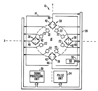
Figure 1 is a top view of : a particular embodiment of a
rotation sensor 10 according to the present invention.
Rotation sensor 10 comprises a base 14 having a cavity 18
etched therein. In this embodiment, cavity 18 is
cylindrically shaped, but many other shapes could be employed.
A plurality of electrodes 22 are radially disposed over a
silicon nitride layer 24 (Fig. 3) which, in turn, is disposed
over the cavity. Each electrode is coupled to a communication
path 26 which, in turn, is coupled to a signal processing unit
30 and to a pulse unit 34. A plurality of Wheatstone bridges
38 are disposed about the periphery of the cavity along the X "
and Y axes shown. Each Wheatstone bridge 38 comprises a
plurality of resistances 42 interconnected in the well known '
manner, and they are coupled to communication path 26 through
a corresponding plurality of communication paths 46. A linear
accelerometer 48, constructed in accordance with the teachings
CA 02145543 2002-O1-30
WO 94/08245 PCT/US93/04935
of U.S. Patent No. 5,284,059, discussed
above, may be formed as a part of the rotation sensor, and
accelerometer 48 may be coupled to communication path 26
through a communication path 50 .
5 In operation, pulse unit 34 applies opposite phase pulses
to pairs of adjacent electrodes 22. The compression and
expansion effect of the opposing electric field between the
adjacent electrodes flex the sector of silicon nitride layer
24 between them. The excitation of adjacent electrode pairs
is continued in a sequential manner radially about the
plurality of electrodes 22 so that the sequential flexures of
silicon nitride layer 24 simulate a high rpm traveling wave
encircling the cavity, thus establishing a net angular
momentum. If the structure rotates about the X axis, then
deformation of the structure about the Y axis occurs as a
result of Coriolus force, and this deformation is sensed by
the Wheatstone bridges disposed along the Y axis. Similarly,
if the structure rotates about the Y axis, then deformation
of the structure about the X axis occurs, and this deformation
is sensed by the wheatstone bridges disposed along the X axis.
The signals from the Wheatstone bridges are then processed by
signal processing unit 30 to pr..oduce a direct indication of
the amount of angular rotation. Signal processing unit 30
also may process the signals from linear accelerometer 48 to
provide an indication of the.amount of linear acceleration of
the structure.
Figures 2-7 illustrate the steps used to fabricate the
rotation sensor shown in Fig. 1.
As shown in Figs. 2 and 3, cylindrical cavity 18 is
formed in base 14 by diffusing an oxide layer or depositing
phosphosilicate glass (PSG) in the shape of a cylinder (or
whatever shape is desired for cavity 18), silicon nitride
layer 24 having a thickness of 1.0 micron to 10.0 microns is
formed over base 14 by chemical vapor deposition, and the PSG
or sacrificial oxide layer is dissolved in a buffered HF
solution. Thereafter, as shown in Figure 4, a titanium and
platinum layer 58 having a thickness of 0.25 to 0.50 micron is
r.
WO 94/08245 ~ ~ ~ PCT/US93/04935
6
deposited over silicon nitride layer 24. Titanium and
platinum layer 58 functions as a uniform conducting ground
plane electrode in the finished device. Next, a ferroelectric
layer 62 having a thickness of 0.2 to 0.5 micron is deposited
by chemical vapor deposition over layer 54. Ferroelectric
layer 62 may comprise a PZT thin film or any other material
having ferroelectric properties which adheres well to titanium
and platinum layer 58.
As shown in Figure 5, the plurality of gold electrodes 22
are then formed by depositing and etching a gold layer having
a thickness of approximately 0.25 to 0.75 micron. Then, as
shown in Figure 6, an insulating silver nitride layer 66
having a thickness of 0.5 micron to 1.0 micron is deposited
over electrodes 22, and a polysilicon layer 70 having a
thickness of 200 to 500 nanometers is deposited over silver
nitride layer 66.
Portions of polysilicon layer 70 disposed about the
circumference of cavity 18 at the intersection of the x and y
axes are then heavily doped with boron to form
piezoresistances 42 and Wheatstone bridges 38. The
polysilicon piezoresistance strain gages achieve wide
temperature range nonlinearity ..and high gage factor. Thus,
the sensing elements are inherently linear, stable, without
zero-rate offset, and without hysteresis. It should also be
noted that the sensing and drive elements are totally
phenomenonically decoupled and independent, so the cross talk
problems associated with using piezoelectric structures for
both the drive and sensing elements (as in quartz sensors) are
avoided.
A silicon nitride layer 74 may be formed over the
structure by pulse enhanced chemical vapor deposition to form
a protective encasement for the device. Silicon nitride layer
74 preferably includes a cavity 78 overlying cavity 18 to
maintain flexibility of silicon nitride layer 24. '
Not only are rotation sensors constructed according to
the teachings of the present invention superior to quartz
rotation sensors , but they also provide advantages in addition
CA 02145543 2002-O1-30
WO 94/08245 PCT/US93/0493~
7
to those found in rotation sensors constructed in accordance
with the teachings of US Patent No. 5,284,059
discussed above. For example, the drive voltage for a
rotation sensor constructed according to the teachings of the
present invention may be approximately three volts (rather
than the much higher voltages required for quartz and other
rotation sensors) which makes the rotation sensor compatible
with on-chip integrated circuits and microprocessors.
Furthermore, even when operating at the low voltages, the
l0 rotation sensor has greater sensitivity to deformation induced
by Coriolus forces than the aforementioned travelling wave
rotation sensor. That is because the maximum energy density
that may be stored in the air gap of the electrostatic drive
in the travelling wave rotation sensor is =eairE2bd where ~ba
is the maximum electric field before breakdown (approximately
108 volts per meter for a one micrometer gap) and where eair
is the permitivity of air which is equal to that of free
space. On the other hand, for ferroelectric layer 62, the
energy density between each electrode and the ground electrode
is ie f~2bd where the maximum ~bd is about the same for
ferroelectric layer 62 as for air but the dielectric constant
ef of ferroelectric layer 62 is approximately 1, 300 times that
of air. This results in three orders of magnitude greater
electric field density, which translates into greater
sensitivity. It is also the.high electric field which causes
silicon nitride layer 24 to flex.
Unlike mechanical gyroscopes or quartz rotation sensors,
the materials and processes employed to fabricate a rotation
sensor according to the present invention are all
semiconductor based, so any electronics, including
microprocessors and self test structures, may be integrated on
the same wafer by further conventional semiconductor
processing. Thus, an entire navigation, guidance or control
subsystem/system can be fabricated on a single chip.
Furthermore, there are no moving or vibrating mechanical parts
and no need for troublesome mechanical mounting structures and
assembly tools as with other rotation sensors. With dimensions
WO 94/08245 ~ 14 ~ ~ ~ ~ PCT/US93/04935
8
on the order of microns, hundreds or thousands of dyes or
complete devices can be fabricated on a single wafer.
While the above is a complete description of a preferred
embodiment of the present invention, various modifications may
be employed. Consequently, the scope of the invention should
be ascertained by the appended claims.