Note: Descriptions are shown in the official language in which they were submitted.
-- 214~~'~~
MAGNETRON ATOMIZATION SOURCE AND METHOD OF USE THEREOF
BACKGRODND AND SUbB~ARY OF THE INVENTION
The present invention relates to a magnetron
atomization source having a target body with a mirror-
s symmetrical, concavely constructed atomization surface with
respect to at least one plane, a magnetic circuit
arrangement operable to generate a magnetic field over the
atomization surface, including an anode arrangement, a
receiving frame which extends around an edge of the target
body and is electrically insulated with respect thereto,
which receiving frame has a receiving opening for at least
one workpiece to be coated, and on the side of the source,
a process space bounded essentially by the atomization
surface of the target body and a surrounding non-atomized
residual interior surface of the receiving frame.
Moreover, the present invention relates to a method of use
thereof in which storage disks, such as CDs, are provided
with an atomization coating.
Magnetron atomization sources are generally described
in DE-OS-24 31 832; EP-A-0 330 445; EP-A-0 311 697; U.S.
Patent No. 5,164,063; and DE-PS-40 18 914.
DE-PS-35 06 227 describes an improved magnetron
atomization source which has one or two target bodies
forming a centrically mirror-symmetrically concavely
-1-
214~~'~0
constructed atomization surface. A workpiece which, in top
view, has a significantly smaller diameter than the
diameter of the cup-shaped target body is inserted by way
of a holding device for the purpose of atomization coating.
Magnetic circuits, which are an arrangement of active
elements such as permanent magnets and/or electromagnets,
as well as of passive elements such as ferromagnetic
elements, for example, of iron yoke parts and air gaps are
provided to generate a magnetic field of the type basically
known in the case of magnetrons. The magnetic circuits
operate separately for the bottom area of the atomization
surface and its arched edge area, respectively.
DE-A-28 24 289 describes the atomization surface of a
target body on a magnetron atomization source in a
centrically concave manner and an earth shielding frame in
the edge area of the target body. With respect to the
target body, the anode is arranged centrically and is
cooled by a medium. In this source, a workpiece to be
coated is generally arranged above the illustrated source.
That is, the workpiece is arranged above the earth
shielding frame which surrounds the edge of the target
body.
EP-A-0 393 957 discloses a magnetron atomization
source which has a centrically concavely shaped-in
atomization surface of the target body. A workpiece to be
atomization-coated is arranged far away from the source.
-2-
21~5~'~
In many cases and specifically also in the case of the
use of the magnetron atomization surface preferred
according to the present invention for the coating of
storage disks, for example, of optical storage disks (such
as magneto-optical disks), video disks or audio disks (such
as compact disks), short coating times with long service
lives of the used target bodies must be achieved. This
requirement has the effect, among other things, that as a
high proportion as possible of the material atomized from
the atomization source is deposited as a coating material
on the workpiece surface to be coated.
Known atomization sources of the type mentioned above
have a disadvantage, however, that, because of, among other
things, the large surfaces which are neither an atomization
surface of the atomization source nor a surface of a
workpiece to be usefully coated, a relatively high
percentage of the material atomized from the atomization
surface of the target is uselessly deposited on other
surfaces defining the process space. This useless
deposition drastically reduces the above-mentioned yield,
and significantly reduces the coating speed as well as the
service life of a target body. As a result, per target
body fewer workpieces can be coated with the given layer
thickness.
In addition, more cleaning intervals are required in
order to ensure operational reliability, and higher
-3-
...,. _
operating power is required to implement desired rates. In
turn, thermal stress to the source and to the workpieces is
increased. All of the foregoing has a negative effect on
the efficiency of a production system.
The above-mentioned disadvantages also apply to the
magnetron atomization source described in DE-A-42 02 349
which has a centrically concavely constructed target body,
a magnetic circuit arrangement which generates a magnetic
field above the atomization surface, an anode arrangement,
and a receiving frame which surrounds the edge of the
target body and is electrically insulated with respect to
it and has a receiving opening for a workpiece disk to be
coated. In this known source, the process space is defined
essentially by the atomization surface of the target body
and the interior surface of the receiving frame. During
operation, the process space is closed off by the workpiece
disk placed on the receiving opening of the receiving
f rame .
Considering the fact that the conventional receiving
frame, as an example of a surrounding non-atomized residual
interior surface, extends on the outside around the edge of
the target body, the length of the cut of the interior
frame surface already visible in the cross-section results
in a large ring surface which is neither usefully atomized
nor usefully coated. It is not significantly smaller than
the new atomization surface of the target body but larger
-4-
than the surface of the receiving opening. Thus, although
a high percentage of the walls bounding the interior
surface of the process space are coated, they are not
usefully coated, thereby still causing lower efficiency.
It is an object of the present invention to eliminate
the above-mentioned disadvantages and to improve
efficiency. This object has been achieved in a magnetron
atomization source in acco=dance with the present invention
by providing that the process space, apart from the
receiving opening for the at least one workpiece, is
bounded essentially by the atomization surface, and
reducing the surrounding non-atomized residual interior
surface to a respective minimum which, during atomization
operation, ensures a stable plasma discharge.
As a result of the fact that, according to the present
invention, the atomization surface of the target body
essentially defines the process space, apart from the
workpiece placed during the operation, a significant
improvement of the ratio between the atomized-off material
quantity and the material quantity deposited as a layer on
the workpiece or the workpieces is achieved and results in
a significant efficiency increase.
Preferred surface ratios are obtained according to the
present invention by providing that the relationship of the
residual interior surface, such as that of the receiving
-5-
214~57~
ring, and that of the atomization surface of the target
body are such the former is less than or equal to 50% of
the latter.
BRIEF DESCRIPTION OF THE DRAWINGS
These and other objects, features and advantages of
the present invention will become more readily apparent
from the following detailed description when taken in
conjunction with the accompanying drawings wherein:
Figure 1 is cross-sectional schematic view of a
currently preferred embodiment of magnetron atomization
source according to the present invention; and
Figure 2 is a view similar to Fig. 1 but supplemented
with magnetic circuits.
DETAINED DESCRIPTION OF THE DRAWINGS
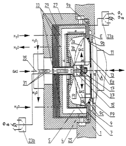
Referring now to Fig. 1, the magnetron atomization
source according to the present invention comprises a
target body 1 having, in a new condition, a conical
atomization surface 3a, or a concave mirror shape 3b,
preferably in the shape of a calotte shell, so that,
already in its new condition with an atomization surface Fl,
the target body 1 is significantly thicker at the edge than
in the center. Although in the illustrated preferred
-6-
~145~70
embodiment the target 1 is circular in top view (not shown)
and therefore its concave shaped-in portion is rotationally
symmetrical, the target body 1 and the following
constructional elements of the source to be described later
may, for certain uses, be constructed to be symmetrical
with respect to a single plane or to two planes. The
target body 1 and therefore the additional construction
elements of the source preferably define a rectangular
magnetron source or an elliptical or generally oval or, in
the illustrated, preferred embodiment, a circular magnetron
source.
In the illustrated circular magnetron source, the
maximal thickness, dl, of the target body 1 on its edge
amounts to approximately 50% of the target radius r1. The
target body 1 is embedded in a ferromagnetic cup-shaped
magnetic circuit housing 4 which defines a cup-shaped
magnet receiving space 5 which encloses the target body 1
on the base side and on its upward-projecting lateral
surfaces. A surrounding receiving frame 9 is provided
along the edge of the target body 1 and of the circular-
ring-shaped end face 7 of the magnetic circuit housing 4
and is electrically insulated from the target body 1 as
well as the housing 4 at a dark space distance. The
interior surface F9 of the receiving frame 9 projects in a
sloped manner from the edge of the target body 1 against
the center axis A of the source inward and defines a
receiving opening 11 for a circular workpiece disk 13. In
the illustrated embodiment, the ratio of the surface F9 to
the new atomization surface F1 is:
F9 < 30% Fl.
The circular workpiece disk 13 is preferably a
dielectric or metallic workpiece disk, preferably the body
of a storage disk to be coated, such as a magneto-optical
storage disk, a video disk, an audio disk such as a compact
disk or CD. The periphery of the disk 13 rests at the edge
of the receiving opening 11 on the receiving frame 9 which,
particularly in the case of CD processing, forms the
peripheral masking element in order to prevent an
atomization coating at the edge of the disk and to obtain
a transition which is as sharp as possible from the coated
surface to the uncoated edge.
The center of the target body 1 can be penetrated by
a core 15, which is electrically insulated with respect
thereto which, however, is not necessary for implementing
the source according to the present invention. For CD-
coating and for coating most other optical storage disks,
the core 15 extends to the level of the receiving opening
plane E in order to mask the center of the workpiece disk
13. If unnecessary for masking or the like, the core 15,
as indicated by the end surface 17, may be reduced in
height or eliminated completely.
_g_
21~~~70
The target body 1 is placed by the magnetic circuit
housing 4 on a negative cathodic potential. As indicated
schematically by the selection units 23a, 23b, the core 15
as well as the receiving ring 9 can be applied to the
anode, such as the ground potential ~o or to adjustable or
fixedly given other reference potentials ~v or can each be
operated in a floating manner. Preferably, the core 15 and
the ring 9 are applied to anodic potentials.
As illustrated, for example, by the insulation ring
9c, two or more parts 9a, 9b can constitute the receiving
frame 9 and optionally be operated electrically in
different ways. For example, an anodic potential can be
applied to part 9a, and part 9b can be operated in a
floating manner.
In the case of a circular workpiece disk 13 with a
radius r13, corresponding to a diameter ~ 13 - 2r13, the
following dimensioning of the maximal distance of the new
atomization surface to the disk surface d1~3 to be coated
has proven to be excellent:
dm3 z 20 0 ~
wherein the distance d113, Particularly in the case of normal
pressure conditions of 10-3 to 10-1 mbar during atomization
coating, should not significantly fall below 25 mm.
_g_
Furthermore, the following dimensioning will
preferably apply: generally, d113 s 50% X13, but preferably:
d113 s 42% X13, and, most preferably, d113 s 35 0
The foregoing dimensioning is particularly true for
the processing of circular-disk-shaped workpieces of
diameters of from 50 mm to 150 mm, particularly 75 mm to
150 mm. If, however, the workpieces to be coated are not
of circular-disk-shape but, for example, are oval or
rectangular, the indicated dimensioning directions with
apply relative to the smallest diameter ~k of the respective
workpiece. Furthermore, it has been found to be
preferable, particularly for CD-coating according to Fig.
1, that the target body radius r1 is 30% to 40% larger than
the radius r13 of the workpiece disk 13 to be coated.
The interior surface F9 of the receiving ring 9 which
is minimized in a sloped manner and which is neither
usefully atomized nor usefully coated and, with respect to
plasma technology, ensures the discharge stability in the
edge area between the disk periphery and the target body
edge, is preferably configured according to the following
dimensioning directions:
The distance e, which is perpendicular with respect to
the axis A or generally with respect to a plane of symmetry
ES and is bridged or spanned by the surface F9, amounts,
relative to the diameter X13 of a circular disk 13 or, more
-10-
--
generally, with respect to the smallest diameter ~k of a
non-circular disk, as defined above, to, generally o s 20%
but preferably to o s 10 0 X13, and currently is most
preferably dimensioned at D ~ 15% ~13-
It is also definitely possible to select the distance a to
be zero. That is, the interior surface F9 is configured to
have only components parallel to the axis A or the plane ES .
The distance, a, bridged or spanned by the interior
surface F9, parallel to the axis A or the plane ES,
irrespective of whether o is or is not larger than zero,
and relative to the distance d113 between the new atomization
surface center and the disk surface to be coated, amounts
to, generally, 0 s a s 50% d113. but preferably to 0 s a s
40o d113, and is currently most preferably dimensioned at a
~ 30o d113
Furthermore, a system-side flange 25 is provided for
mounting the source according to the present invention. An
electric insulation 29 is provided between a source housing
27 with the flange 25 and the magnetic circuit / target
body arrangement comprising the housing 4 and the target
body 1. In addition, as illustrated schematically, the
centric core 15 is medium-cooled, preferably water-cooled,
by way of a pipe system 31. The cooling of the receiving
frame 9 takes place by way of the flange 25.
-11-
_ 21~5~'~0
The cathode/anode discharging distance may be operated
by an AC- and DC-mixed supply, for example, by a timed DC,
or may be operated only by DC. Layers may be deposited
reactively or non-reactively, preferably from electrically
conducting target body material. As also illustrated
diagrammatically by the pipe system 33, the magnetic
circuit housing 4 and the target body 1 are medium-cooled,
preferably water-cooled.
A working gas (for non-reactive atomization coating,
this gas may be a noble gas or for reactive atomization
coating, this gas may be a noble gas with a reactive gas,
the latter reacting with the material atomized from the
target body 1, and the coating taking place by a reaction
product) is preferably discharged by a schematically
illustrated pipe system 35 in the core 15 via outlet
openings 37 into the process space as shown by the radially
directed arrows.
In Fig. 2, which for reasons of clarity is the same
representation as Fig. 1, a currently preferably
implementing magnetic circuit is entered in the housing 4.
A ring of permanent magnets 40 is arranged in the area of
the face 7 of the ferromagnetic housing 4. In the center
and approximately on half the radius, r1, of the atomization
surface, additional permanent magnet rings 42 and 41 are
provided.
-12-
2145~'~0
As indicated, the polarities of the ring magnets are
selected such that, qualitatively, the magnetic field B
illustrated in Fig. 2 is created above the atomization
surface and essentially, as the atomization increases,
maintains the same strength and the same direction with
respect to the momentary atomization surface. Naturally,
it is also easily possible, for example, by way of a
mechanical following of the magnet ring 40 and/or 41, to
cause the magnetic field during the atomization to follow
the respective momentary atomization surface in an
optimized manner. The face 7 is covered by a layer 8 of a
non-ferromagnetic material (for example, an insulating
material), such as a high-temperature resistant and vacuum-
suitable plastic material. This layer 8 is, on the side,
disposed against the dark space 8a and, on the other side,
above the one magnetic pole N. As a result, parasitic
plasma discharges and flashovers, which may be triggered in
the dark space by strong magnetic fields, are prevented.
With the magnetic field B constructed according to the
present invention, it is also ensured that, also at the
edge of the target body 1, an atomization removal takes
place as much as possible to largely prevent an atomization
accumulation there. Also, in the center of the target body
1, the zone in which no atomization removal takes place,
~25 also the amount of the atomized-on material is minimized.
-13-
- _214~5~r~
The active elements 40, 41, 41 provided in the hollow
space 5 and the non-active elements, such as the iron
housing 4 and the geometrical arrangement with its air gaps
44, contribute significantly to the construction of the
magnetic field B of Fig. 2.
Because the receiving frame 9 shown in Fig. 1 can be
electrically operated arbitrarily within wide ranges, and
a center masking can be implemented also by a center mast
50, without providing a core 15, it is now possible with
certainty to bring the frame 9 implementing the edge
masking in a changed construction and/or the center mask
50, as explained in detail in German Patent Application 42
35 678, together with the workpiece disk in the respective
coating position.
With a magnetron sputter source implemented as shown
in the example, having a target diameter of 160 mm, a
substrate diameter of 120 mm, a target/substrate distance
d113 of 35 mm, a new atomization surface shape: concave,
spherical shell with r = 80 mm, a power supply of 15 kW,
permanent magnets made of neodymium, ferrite, a pressure of
approx. 10-z mbar, and.a target material of A1 (Mg, Si, Mn)
service lives of 80,000 coated CDs were achieved,
corresponding to 220 kWh.
The specific coating rate, defined as the coating rate
per power unit (kW), in the case of the new atomization
-14-
- _ 2145~7~
surface, amounted to 7 nm/kWs and, at the end of the
service life, was still 4.5 nm/kWs. The coating was
carried out with a thickness of 55 nm. Here, 52% of the
material atomized off the target body arrived as coating
material on the workpiece disks. The outer edge zone of
the target body, which was not atomized off, amounted to 3
mm. In the center, this zone amounted to less than 1 mm,
usually 0 mm. In these zones, the maximal atomization
quantity during the target life or service life amounted to
approximately 500 ~,m.
Thus, with the magnetron source according to the
present invention, a high average coating rate is achieved
with long service lives while the surface coating is
perfectly uniform and has high efficiency, whether defined
as a coating quantity per atomized material quantity or as
a layer quantity per electric energy unit, in which case
all process parameters can be maintained essentially
constant during the service life of the target body. The
specific coating rate was increased virtually to a factor
of 2 compared with known sources.
Although the invention has been described and
illustrated in detail, it is to be clearly understood that
the same is by way of illustration and example, and is not
to be taken by way of limitation. The spirit and scope of
the present invention are to be limited only by the terms
of the appended claims.
-15-