Note: Descriptions are shown in the official language in which they were submitted.
~ . 21~562-2
~ ~,
Q~ADRATURE MODULATOR OPERABLE IN Q~ASI-MICROWAVE
BAND OF DIGITAL COMMUNICATION SYSTEM
BACKGROUND OF THE INVENTION
1. Field of the Invention
The present invention generally relates to a quadrature
modulator. More specifically, the present invention is
directed to a quadrature modulator for a digital
communication suitable to a phase modulation of a high
frequency signal such as in a quasi-microwave signal band.
2. Description of Prior Art
Conventionally, quadrature modulators used in such a
high frequency band as a quasi-microwave band have been
constructed by way of semiconductor integrated circuits.
For instance, "QPSK Modulators for Digital Cellular
Communication" of Bipolar Circuits and Technology Meeting
3.2, IEEE, 1992,- pages 59 to 62 describes the quadrature
modulator as shown in a circuit diagram of Fig. 1.
As represented in Fig. 1, in this prior art quadrature
modulator, the QPSK-modulated wave is obtained by phase-
shifting the local oscillating signal LOl by phase shifter
65 to produce a first signal and a second signal having a
phase sifted by 90 degrees from that of the first signal.
Thereafter, the first signal is supplied to mixer 66 so as
to be multiplied with the in-phase signal "I" having the
phase opposite to that of this first signal. On the other
-1-
2145622
hand, the second signal is supplied to mixer 67 in order to
be multiplied with the quadrature signal "Q" having the
phase opposite to that of the second signal. Then, these
multiplied output signals are supplied to synthesizing
amplifier 68 so as to be synthesized with each other,
thereby producing the QPSK modulated wave. After only the
required frequency component of this QPSK modulated wave has
been filtered out by filter circuit 69 having the bandpass
filter characteristic, this filtered frequency component is
furnished to mixer 70. In the mixer 70, this filtered
frequency component is mixed with another local oscillating
signal LO2 to be frequency converted, so that the resultant
signal is obtained as the quasi-microwave band signal.
Then, further, this quasi-microwave band signal is processed
in output amplifier 71 and balance-unbalance converting
circuit 72 to be outputted.
Another conventional quadrature modulator, as indicated
in a block diagram of Fig. 2, is disclosed in "DIGITAL
PHASE-SHIFT QUADRATURE FRONTED FOR LO-INPUTS UP TO 6 GHz"
written by P. Weger et. al., Publication of 20th Europe
Microwave Conference, 1990, page 426.
As indicated in Fig. 2, 90-degree phase shifter 80 is
constructed of mixer 81 and two sets of 1/2 frequency
dividers 82 and 83 in the conventional quadrature modulator.
In this quadrature modulator, the input signal is multiplied
by the local oscillating signal LO by the mixer 81 to obtain
the signals having the phases opposite to each other and the
--2--
2195622
frequencies two times higher than that of the input signal.
These output signals are divided by 1/2 in the frequency
dividers 82 and 83, so that such carrier signals LOQ and LOI
are outputted, which have the phases different from each
other by 90 degrees and also the same frequencies as that of
the above-described local oscillating signal LO. Mixers 84
and 85 multiply modulating signals IFQ and IFI by the carrier
signals LOQ and LOI to output the multiplied signals RF as
the quadrature modulated waves.
In the conventional quadrature modulator shown in Fig.
2, the 90-degree phase shifter 80 is manufactured by the
silicon transistors as the semiconductor integrated circuit.
On the other hand, other quadrature modulators manufactured
by such compound semiconductors as GaAs as an integrated
circuit are conventionally known from, for example, "A 1.9-
GHz-Band GaAs Direct-Quadrature Modulator IC with a Phase
Sifter" by K. Yamamoto et al., IEEE JOURNAL OF SOLID-STATE
CIRCUITS", VOL. 28, No. 10, October 1993, pages 994 to 1000.
Fig. 3 is a circuit diagram for showing the quadrature
modulator manufactured from the compound semiconductor as an
IC form, which is disclosed in the above-described
publication. This conventional modulator is arranged by 90-
degree phase shifter 91, driver 92, and mixers 93 and 94.
The driver 92 owns biasing capacitors C1 and C2 at the front
stage, and is constructed in such a way that three stages of
the differential amplifiers with employment of the field-
effect transistor made of GaAs are cascade-connected. The
--3--
2145622
carrier signals having the different phases from each other
by 90 degrees are inputted from the 90-degree phase shifter
91 into this driver 92 to be amplified by the driver 92.
Then, the amplified carrier signals are supplied to the
mixers 93 and 94 in which these amplified carrier signals
are multiplied with the modulating signal.
Also, there have been conventionally proposed the
methods for correcting the phase errors of the 90-degree
phase shifter in, for instance, Japanese Patent Disclosures
No. 61-238144 (1986), No. 2-174343 (1990), and No. 4-287542
(1992). As an example, the circuit block diagram of the
quadrature modulator described in Japanese Patent Disclosure
No. 2-174343 is indicated in Fig. 4. In accordance with the
conventional quadrature modulator shown in Fig. 4, the
carrier signal entered from input terminal 99 is divided
- into two divided carrier signals by divider 100. One
divided carrier signal is supplied to mixer 103 so as to be
multiplied with the first modulation signal supplied from
input signal 101, whereas the other divided carrier signal
is phase-shifted by 90 degrees in variable phase shifter
105, and the phase-shifted carrier signal is supplied to
mixer 104 so as to be multiplied with the second modulation
signal derived from input terminal 102. The respective
output signals from the mixers 103 and 104 are combined with
each other in combiner 108, and then the combined signal is
supplied as the QPSK modulated carrier to output terminal
109 .
- 2145622
In addition to the above-described general circuit
arrangement, phase comparator 106 of this conventional
quadrature modulator compares the phases of these divided
carrier signals to detect how degree the phase difference
between them is shifted from the original 90 degrees. The
signal representative of this detected phase difference is
supplied via loop filter 107 to the variable phase shifter
105 as the control signal, so that the phase shift amount of
the variable phase shifter 105 is variable-controlled in
such a manner that the phase difference between the output
signals from the mixers 103 and 104 can be equal to 90
degrees.
Further, another conventional quadrature modulator is
known from Japanese Electronic Information Communication
Institute, Spring Conference C-80 in 1993, in which the 90-
degree phase shifter operable in the quasi-microwave band is
constructed of the passive circuit operable under no power
consumption, as represented in Fig. 5. In this prior art
quadrature modulator, inter digital type 90-degree phase
shifter 112 is employed on the substrate 111. The carrier
signal inputted via terminal 113 is converted by the 90-
degree phase shifter 112 into the first carrier signal and
the second carrier signal having the different phase from
that of the first carrier signal by 90 degrees. The first
and second carrier signals are supplied to two-phase
modulators 114 and 115, which are manufactured as the
integrated circuit, and are modulated by the modulation
--5--
2145622
signals derived from terminals 116 and 117. The signals
outputted from the 2-phase modulators 114 and 115 are
processed in the combiner formed on substrate 118 and the
processed signals are outputted from output terminal 119 as
the QPSK ( quadrature phase shift keying ) modulated signal.
In this conventional quadrature modulator, the inter
digital type 90-degree phase shifter 112 is formed on the;
alumina ceramics substrate 111 as the thin film circuit, and
both of this alumina ceramics substrate 111 and the
substrate 118 are assembled with the two-phase modulators
114 and 115 into a single package, so that this quadrature
modulator is operable over such a wide frequency band of 1.5
GHz under less power consumption.
In addition, a further quadrature modulator operable in
the quasi-microwave band is known from japanese Patent
Disclosure No. 5-347529 opened on December 27, 1993, in
which the phase shifter is arranged by the passive element.
Fig. 6 is a circuit diagram for showing one example of the
phase shifter employed in this conventional quadrature
modulator. In this drawing, the 90-degree phase shifter is
so arranged that the first phase shifter constructed by
cascade-connecting first phase shifting unit 121a and first
differential amplifier circuit 122a is connected in parallel
to the second phase shifter constructed by cascade-
connecting second phase shifting unit 121b and second
differential amplifier circuit 122b with respect to the
input.
--6--
2145622
Each of these phase shifting units 121a and 121b is
constructed of the series circuit between the two 4-terminal
phase shifters.- These phase shifters are formed on the
semiconductor substrate from the spiral coil functioning as
the phase leading element and the MIM (Metal Insulator
Metal) capacitor functioning as the phase delaying element.
The high frequency input signals RF1 and RF2 having the
phases opposite to each other are inputted via the input
terminal to these phase shifting units 121a and 121b, and
then are phase-shifted by the phase shifting units to
produce two sorts of signals S2A, S2B and S4A, S4B which are
represented by quadrature vectors. It should be noted in
th-is case that the phase shifting amounts of the phase
shifting units 121a and 121b are set in such a manner that
combined vector S2 between the signals S2A and S2B is
substantially perpendicular to combined vector S4 between
the signals S4A and S4B.
The above-described signals S2A, S2B, and S4A, S4B are
entered into the gates of the differential-paired
transistors in the differential amplifiers 122a and 122b
provided at the next stage, and are differentially amplified
by these differential amplifiers, whereby the resulting
amplified signals are outputted as signals VlA, VlB and V2A,
V2B from the in-phase output terminal and the inverse output
terminal, respectively. It should be understood that the
phase of the output signal VlA is different from that of the
output signal V2A by 90 degrees, whereas the phase of the
--7--
2145622
output signal VlB is different from that of the output
- signal V2B by 90 degrees.
Accordingly to this conventional phase shifter, as
indicated in Fig. 7, the signals VlA (VlB) and V2A (V2B)
whose phases could be shifted in precision of (90 - 2 ) to
(90 + 2 ) can be produced with respect to the high
frequency input signals RF1, RF2 in the frequency range from
700 MHz to 2 GHz.
As to the above-described conventional quadrature
modulator of Fig. 1, after the input signals (local
oscillator signals) are modulated by the low frequency
signal, the modulated signals are frequency-converted into
the quasi-microwave signals in the mixer 70. As a result,
there are drawbacks that two sorts of signal sources LO1 and
LO2 are required, the complex circuit arrangement is needed,
and spurious noise is produced.
As to another conventional quadrature modulator shown
in Fig. 2, although only one signal source LO is required,
the 90-degree phase shifter manufactured by the bipolar
transistor in the semiconductor integrated circuit could not
be practically operated with the carrier frequencies higher
than 1 GHz even when this 90-degree phase shifter is
realized by the circuit arrangement 80 shown in Fig. 2, or
other circuit arrangéments. Namely, this quadrature
modulator cannot be used in the quasi-microwave band. To
the contrary, even when this quadrature modulator is
operable in such a quasi-microwave band, since active
--8--
- ' 21~5622
-
circuit elements are employed, there is another problem that
this conventional quadrature modulator would consume high
power.
Also, in the conventional quadrature modulator
indicated in Fig. 3, since the 90-degree phase shifter 91
utilizes the filter circuit constructed of the resistor and
the capacitor, such amplifier 92 whose output level becomes
constant is required to correct unbalance in the output
levels. Therefore, there is another problem that the power
consumption is increased. A further problem exists in that
since the field-effect transistor of the compound
semiconductor is more expensive than the silicon bipolar
transistor, the overall cost of this quadrature modulator
would be increased.
Then, another conventional quadrature modulator
represented in Fig. 4 employs such a method for improving
the phase shifting precision of 90 degrees in such a manner
that the phase shifter is constructed of the variable phase
shifter 105, and the phase error detected by the phase
comparator 106 is fed back to the variable phase shifter
105. However, there is no concrete description about the
operation frequency of the variable phase shifter 105 in
Japanese Patent Disclosure No. 2-174343, and thus this
conventional quadrature modulator cannot be used in the
quad-microwave band.
On the other hand, although the power consumption of
the conventional quadrature modulator is low, high
_g_
2145622
manufacturing precision is required for the pattern of the
thin film circuit used to constitute the inter digital type
90-degree phase shifter 112 on the substrate 111.
Accordingly, there are such drawbacks that this quadrature
modulator becomes high cost, and such a cumbersome bonding
work is required to connect the very narrow patterns to each
other by employing such a fine wire as a gold wire.
Moreover, there are other drawbacks. That is, since the
semiconductor integrated circuit chips of the substrates
111, 118 and the two-phase modulators 114, 115 are connected
to the package by the adhesive soldering material, very
cumbersome works are needed. In addition, the cost and
volume of this quadrature modulator would be increased.
Furthermore, when the phase shifter of the conventional
quadrature modulator represent in Fig. 6 is manufactured on
the semiconductor integrated circuit, it is difficult to
employ such a manner to construct the spiral coil with a
desirable constant. Therefore, as a so-called "cut and try"
method is necessarily required to manufacture the desirable
spiral coil, there is another drawback that a lengthy
designing process is needed. Also, since large fluctuation
is made in the constants of the spiral coil and the MIM type
capacitor due to the integrated circuit itself, the
resulting 90-degree phase difference is greatly fluctuated.
Moreover, when such a spiral coil having the constant of
several hundreds nH is constructed, a large area is
required, which may cause problems that the overall volume
-10-
- ' 2145622
-
of this quadrature modulator is increased and the high cost
thereof is needed.
Additionally, as apparent from the characteristic shown
in Fig. 7, the phase shifter of the conventional quadrature
modulator owns errors with + 2- to - 2- in the frequency
range from 700 MHz to 2 GHz. Taking account of the
fluctuation, the entire errors would be further increased.
Further, such a band width of 1.3 GHz where a desired phase
shift could be achieved would be an insufficient band width
in view of various usage in the quasi-microwave band.
BRIEF SUMMARY OF THE INVENTION
The present invention has been made to solve the above-
described various problems, and therefore, has an object to
provide a quadrature modulator capable of reducing wrapping
around of an input signal into an output terminal, in which
an input level is lower over a wide frequency bandwidth of
such a high frequency band as a quasi-microwave band.
Another object of the present invention is to provide a
compact quadrature modulator manufactured at low cost.
SUMMARY OF THE INVENTION
To achieve the above-described object, a quadrature
modulator for modulating a phase signal in a high frequency
band, according to one aspect of the present invention,
comprises:
a multi-layer substrate for constituting a 90-degree
phase shifter at an inner layer of said multi-layer
substrate, said 90-degree phase shifter subdividing an input
--11--
' 2145622
carrier signal into a first carrier signal and a second
carrier signal having a phase different form that of said
first carrier signal by 90 degrees by a distributed coupling
circuit;
a semiconductor integrated circuit containing therein
two sets of 2-phase modulating circuit units and connected
via a wiring line to said multi-layer substrate, said 2- :
phase modulating circuit units modulating said first carrier
signal and said second carrier signal, derived from said 90-
10' degree phase shifter, based on an externally inputted
modulating signal, thereby outputting quadrature-modulated
signals; and
protection means for protecting said semiconductor
integrated circuit and said wiring line for protection
purposes.
The quadrature modulator of the present invention can
~ be made compact by arranging the above-described multi-layer
substrate which includes at least:
- a first substrate located at an uppermost layer of said
multi-layer substrate and having a region on which said
semiconductor integrated circuit is mounted and fixed, a
wiring pattern for connecting a pad of said semiconductor
integrated circuit via a wiring line to a terminal of said
90-degree phase shifter being formed on said first
substrate;
a plurality of second substrates located at an
intermediate layer of said multi-layer substrate and
-12-
21~5622
connected to different input terminals for the carrier
signals, said distributed coupling circuit being constituted
by the wiring patterns formed between the upper second
substrate and the lower second substrate; and
a third substrate located at a lowermost layer of said
multi-layer substrate, for forming a ground plane.
~ The quadrature modulator of the present invention can
be manufactured at low cost by arranging the above-described
multi-layer substrate which includes at least:
~10 a first substrate located at an upper layer of said
multi-layer substrate and having at least a first wiring
pattern for connecting a pad of said semiconductor
integrated circuit via a wiring line to a terminal of said
90-degree phase shifter, a region on which said
semiconductor integrated circuit is mounted and fixed, and a
second wiring pattern whose one ends are connected to
different input terminals for the carrier signals, for
constituting a side coupling type of said distributed
coupling circuit; and
a second substrate .located at a lower layer of said
multi-layer.substrate, for constituting a ground plane.
According to.the present invention, since the 90-degree
phase shifter is constructed of the multi-layer substrate
and the semiconductor integrated modulator circuit
containing the 2-phase modulating circuit unit is mounted on
this multi-layer substrate, the overall quadrature modulator
can be formed within the same area as the multi-layer
-13-
- 2145622
.
substrate. Also, since the 90-degree phase shifter is
arranged by the distributed coupling circuit by the multi-
layer substrate, both of the phase error and the difference
between the passing loss and the coupling loss of the 90-
degree phase shifter can be lowered over the wide high
frequency band.
BRIEF DESCRIPTION OF THE DRAWINGS
The above-described objects and other objects,
features, and als,o advantages of the present invention will
become more apparent by reference to the following detailed
description of the present invention taken in conjunction
with the accompanying drawings, wherein:
Fig. 1 is a circuit diagram for showing an example of
one conventional quadrature modulator;
Fig. 2 is a schematic block diagram for representing
another conventional quadrature modulator manufactured by
the bipolar transistor in the semiconductor integrated
circuit form;
Fig. 3 is a schematic block diagram for indicating
another conventional quadrature modulator manufactured by
the compound semiconductor in the semiconductor integrated
circuit form;
Fig. 4 schematically represents the circuit arrangement'
of another conventional quadrature modulator having the
phase error correcting means;
Fig. 5 schematically indicates the circuit arrangement
of another conventional quadrature modulator equipped with
-14-
. ~ 2145622
the 90-degree phase shifter constructed of the passive
circuit;
Fig. 6 is a schematic circuit diagram of the phase
shifter constructed of the passive element employed in
another conventional quadrature modulator;
Fig. 7 graphically shows the phase-to-frequency
characteristic diagram of the phase shifter shown in Fig. 6;
Fig. 8 is a perspective view for showing a quadrature
modulator according to a first embodiment of the present
invention;
Fig. 9 is a plan view of the first layer of the
substrate employed in the quadrature modulator shown in Fig.
8;
Fig. 10 is a plan view of the m-th layer of the
substrate employed in the quadrature modulator shown in Fig.
8;
Fig. 11 is a plan view of the (m+l)th layer of the
substrate employed in the quadrature modulator shown in Fig.
8;
Fig. 12 is a plan view of the (n+l)th layer of the
substrate employed in the quadrature modulator shown in Fig.
8;
Fig. 13 is a schematic circuit diagram for showing the
quadrature modulator of Fig. 8;
Fig. 14 graphically indicates a characteristic
representation between passing loss-and coupling loss in the
quadrature modulator of Fig. 8;
-15-
2145622
Fig. 15 graphically indicates a characteristic
representation among passing output, coupling output, and
phase difference in the quadrature modulator of Fig. 8; and
Fig. 16 is a plan view for showing another quadrature
modulator according to a second embodiment of the present
invention.
DETAILED DESCRIPTION OF THE PREFERRED EMBODIMENTS
A detailed description will now be made of
quadrature modulators according to various preferred
embodiments of the present invention.
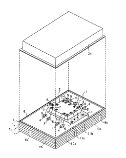
Fig. 8 is a perspective view for showing a quadrature
modulator according to a first embodiment of the present
invention. Figs. 9 to 12 are plan views for representing
various layers of the substrate shown in Fig. 8.
As schematically indicated in Fig. 8, the quadrature
modulator according to this embodiment is mainly arranged by
a multi-layer substrate 1 into which a 90-degree phase
shifter is assembled, a semiconductor integrated modulator
circuit 2 into which two sets of 2-phase modulators and an
output signal synthesizing circuit are assembled, and a lid
24.
The multi-layer substrate 1 is constructed of n layers
of substrates, i.e., from a first layer (uppermost layer) of
substrate 11 to an n-th layer (lowermost layer) of substrate
ln~ A wiring plane is constructed of an (n-l)th layer. A
surface layer formed on the first layer of substrate 11
corresponds to either a layer for assembling a semiconductor
-16-
214~622
,~,
integrated circuit, or a layer for connecting the substrate
with the semiconductor integrated circuit. As represented
in the plan view of Fig. 9, there are formed in the first
layer of substrate 11, a rectangular wiring pattern 3, each
of island-shaped wiring patterns 5 formed around this
rectangular wiring pattern 3, and a pattern 6 having a
narrow-width and formed along the peripheral portion of this
substrate, which may seal a lid 24. Furthermore, via holes
4 are formed at a predetermined position of the wiring
pattern 3 and the wiring pattern 5 in order to be
electrically connected to the under layer of substrate.
As a result, a semiconductor integrated circuit 2 is
mounted and fixed on the wiring pattern 3 of the first
layer's substrate 11, and a terminal pad of the semiconductor
integrated circuit 2 is connected to the corresponding
- wiring pattern 3 or 5 by way of a bonding wire (wiring line)
7 such as gold (see Fig. 8).
To a side portion and a bottom portion of the multi-
layer substrate 1, carrier signal input terminals 8a and 8b,
four input terminals 9a to 9d for modulation signals (only
two input terminals 9a and 9b being illustrated in Fig. 8),
two high frequency ground terminals lOa and lOb (only one
ground terminal lOa being illustrated in Fig. 8), are formed
as the wiring pattern forms. Further, five ground terminals
lla to lle (only two ground terminals llb and llc being
represented in Fig. 8), a power supply terminal 12 (not
shown in Fig. 8), and an output terminal 13 are formed in
-17-
2145622
the wiring patterns on the side portion and the bottom
portion of this multi-layer's substrate.
It should be noted that reference numerals of the
above-described respective terminals are indicated within
parentheses, which are connected through the via holes 4 to
the wiring pattern 5 on the plan view of the first layer
shown in Fig. 9. Also, the ground terminals lla to lle are
connected through the via holes 4 in the wiring pattern 3.
As indicated in the plan view of Fig. 10, both of a
substantially U-shaped wirlng pattern 14 one end of which is
connected to the above-explained carrier signal input
terminal 8a, and another wiring pattern 15 one end of which
is connected to the above-described power supply terminal 12
are formed in the m-th layer on the m-th substrate lm
corresponding to the intermediate layer of the multi-layer
substrate 1. Also, via holes 16 are formed in both ends of
the wiring pattern 14, and via holes 17 are formed in both
ends of the wiring pattern 15.
As shown in the plan view of Fig. 11, a wiring pattern
18 for connecting two via holes to each other, one end of
which is connected to the carrier signal input terminal 8b,
is connected on an (m+l)th layer of the (m+l)th substrate
lm+l of the multi-layer substrate 1. A wiring portion 18a
located at a center portion of the substrate of this wiring
pattern 18 is formed at a wiring portion 14a located at a
center portion of the substrate lm and a position near the
substrate along the vertical direction. These wiring
-18-
2145622
patterns 14a and 18b constitute the 90-degree phase shifter
made of distributed coupling circuits with lengths of
approximately ~g/4. It should be noted that symbol "~g"
indicates a wavelength on a signal line, which is determined
by a thickness and the dielectric constant of a substrate.
Generally speaking, a wavelength of a center frequency in
the used frequency range is selected as this wavelength
,.~g
Furthermore, as shown in the plan view of Fig. 12, a
wiring pattern 20 connected to the respective ground
terminals lla to lle, and a wiring pattern 22 separately
connected to the above-described terminals 8a, 8b, 9a to 9d,
lOa, lOb, 12, and 13 are provided on an (n+l)th layer of a
lower-sided surface of the n-th substrate ln (namely,
lowermost layer) of the multi-layer substrate 1. A via hole
21 used for electrically connecting to the upper layer
substrate is fabricated in the wiring pattern 20, whereas a
via-hole 23 used for electrically connecting to the upper
layer substrate is formed in the wiring pattern 22.
The terminals 8a, 8b, 9a to 9d, lOa, lOb, lla to lle,
12 and 13 are formed on the multi-layer substrate 1
constructed of the wiring layers 1 to (n+1) of the
substrates 11 to ln with the above-described structures.
After the semiconductor integrated circuit 2 has been
mounted on the multi-layer substrate 1 and connected
theréto, as illustrated in Fig. 8, the lid 24 is provided so
as to protect the semiconductor integrated circuit 2 and the
--19--
.~ 2145622
bonding wire 7. Alternatively, to protect the semiconductor
integrated circuit 2 and the bonding wire 7, a resin
material may be coated thereon instead of this lid 24.
A circuit of the quadrature modulator with the above-
described structure according to this first embodiment is
represented as a circuit diagram of Fig. 13. It should be
noted that the same reference numerals shown in Fig. 8 to 12
are employed as those for denoting the same or similar
circuit elements in this Fig. 13. In Fig. 13, the
semiconductor integrated circuit 2 is arranged by comprising
mixers 26a, 26b for constituting a 2-phase modulator, and a
synthesizing (combining) circuit 27. In Fig. 13, the power
supply terminal 12 and the ground terminals lla to lle are
omitted.
Next, a description is made of operations of this
quadrature modulator with reference to Fig. 13. A carrier
signal is entered into one of the input terminals 8a and 8b,
and the other input terminal is connected via a terminal
resistor and a capacitor to the ground plane, thereby being
grounded in view of high frequency circuitry. The carrier
signal supplied from the input terminal 8a or 8b is divided
by the distributed coupling circuit constructed of the
above-described wiring patterns 14 and 18 into two (first
and second) carrier signals having different phases from
each other by 90 degrees, and thereafter these divided
carrier signals are supplied to the mixers 26a and 26b. In
the mixer 26a, the first carrier signal inputted is
-20-
' 2145622
multiplied by first modulation (modulating) signals having
phases opposite to each other and furnished from the input
terminals 9c and 9d. In the mixer 26b, the second carrier
signal having such a different phase from that of the first
carrier signal by 90 degrees is multiplied by second
modulation (modulating) signals having phases opposite to
each other and supplied from the input terminals 9a and 9b.
Reference numerals lOa and lOb represents capacitors which
are grounded in view of high frequency circuitry.
The synthesizing circuit 27 synthesizes the 2-phase
modulation (modulated) signal-obtained from the mixers 26a
and 26b by way of the multiplication, and the resulting 4- -
phase phase modulated signals are outputted from the output
terminal 13.
Fig. 14 is a graphic representation of a characteristic
curve between passing loss and coupling loss occurred in the
quadrature modulator of this first embodiment. The abscissa
of Fig. 14 indicates the frequency, whereas the ordinate
thereof represents the gain and isolation. In this graphic
representation, a curve "I" shows the gain (passing loss) of
the signal transmission path achieved from the carrier
signal input terminal 8a (8b) to the input terminal of the
mixer 26b (26a), another curve "II" denotes isolation
(coupling loss) between both of the input terminals of the
mixers 26a and 26b, and also another curve "III" represents
a coupling amount of a signal from the input terminal 8a
(8b) to the mixer 26a (26b) under such a condition that the
-21-
21~5622
center frequency is selected to be 2.4 GHz.
On the other hand, Fig. lS shows another graphic
representation in which the ordinate indicates a phase
difference between a passing output and a coupling output in
this first embodiment. Namely, this ordinate shows such a
phase difference between the carrier signals supplied to the
input terminals of the mixers 26a and 26b. The abscissa
denotes the frequency.
As apparent from the curves I and III shown in Fig. 14,
the frequency bandwidth where the difference between-the
passing loss and-the coupling amount is below 1 dB
corresponds to 1.25 GHz defined from 1.85 GHz to 3.10 GHz.
At this time, an angular shift from 90 degrees in the phase
difference between the passing output and the coupling
output is smaller than, or equal to 1 degree, as illustrated
in Fig. 15. It could be understood from the foregoing
description that the above-explained quadrature modulator
according to the first embodiment is operable over such a
wide frequency range. Furthermore, as obvious from the
graphic representation of Fig. 15, the frequency bandwidth
where the angular shift from 90 degrees in the above-
explained phase difference becomes smaller than, or equal to
2 degrees corresponds to approximately 3 GHz, namely this
frequency bandwidth is very broader than that of the
conventional quadrature modulator.
It should be noted in this measurement example that as
shown in the curve III of Fig. 14, the m~x;mum coupling
-22-
~ 2145622
amount is approximately - 3.5 dB, whereas the minimum
passing loss amount is about - 3 dB as shown in the curve I.
When the difference between the maximum coupling amount and
the minimum passing loss amount is selected to be 1 dB in
order that the maximum coupling amount becomes larger than
this difference, such a bandwidth that the difference
between the passing loss and the coupling amount is smaller
than, or equal to 1 dB becomes wide, so that it is possible
to constitute such a 90-degree phase shifter operable over
the quasi-microwave band from 1 GHz, in which few input
signals are wrapped around the output signal.
In accordance with the first embodiment, as apparent
from Fig. 8, since the quadrature modulator is so arranged
by assembling the 90-degree phase shifter by employing the
multi-layer substrate 1 and also by assembling two sets of
2-phase modulators and the output signal in-phase
synthesizing circuit by employing the semiconductor
integrated modulator circuit 2, these 90-degree phase
shifter, semiconductor integrated modulator circuit chip,
and other wiring patterns can be fabricated on the same
area. Also, the multi-layer substrate and the package can
be incorporated in one body. As a consequence, the more
compact quadrature modulator can be manufactured at low cost
and operable under low power consumption, as compared with
the conventional quadrature modulator.
Subsequently, a quadrature modulator according to a
second embodiment of the present invention will now be
-23-
2145622
described. In Fig. 16, there is shown as a plan view the
quadrature modulator of the second embodiment. In
accordance with this second embodiment, a 90-degree phase
shifter is constructed of a two-layer substrate, and since
the second layer constitutes the ground plane, a wiring
pattern is formed only on the first layer. Fig. 16
represents the wiring pattern formed on this first layer.
In other words, there are fabricated on a first substrate
311, a semiconductor integrated modulator circuit 32 for
assembling therein two sets of 2-phase modulators and the
output signal in-phase synthesizing (combining) circuit, a
rectangular wiring pattern 33, and island-shaped wiring
patterns 34a to 38 formed around this rectangular wiring
pattern 33 in a separate form. Furthermore, wiring patterns
39 to 41 and a region 43 having a narrow width and formed
along the peripheral edge of this first substrate 311 are
formed on the first substrate 311.
As illustrated in Fig. 16, the semiconductor integrated
circuit 32 is mounted and fixed on the wiring pattern 33,
and the wiring patterns 34a to 38 corresponding to the
terminal pads of the semiconductor integrated circuit 32 are
connected by a bonding wire 44 such as gold. It should be
noted in this second embodiment that the wiring patterns 34a
and 34b are wiring patterns to be connected to an input
terminal of a first modulation signal, and the wiring
patterns 35a and 35b correspond to wiring patterns to be
connected to an input terminal of a second modulation
-24-
2145622
signal. Furthermore, the wiring pattern 36 is a wiring
pattèrn to be connected to a power supply terminal, the
wiring patterns 37a and 37b correspond to wiring patterns to
be connected to a high frequency ground terminal, and also
the wiring pattern 38 is a wiring pattern to be connected to
an output terminal. Then, as indicated by black solid
circles of Fig. 16, via holes are formed in the edge
portions of these wiring patterns on the substrate side.
Another wiring pattern 39 one end of which is connected
through a via hole 45 to an input terminal of a first
carrier signal and the other end of which is connected via a
bonding wire 46 to a preselected terminal pad of the
semiconductor integrated modulator owns a narrow center
portion and is formed in a zigzag form. On the other hand,
another wiring pattern 40 has one end connected through a
via hole 47 to an input terminal of a second carrier signal,
and the other end located at a center portion of the
substrate as well as a narrow width indicated by reference
numeral 40a. One end of a wiring pattern 41 has a narrow
width and also is located at a center portion of the
substrate (indicated by reference numeral 41a), whereas the
other end of this wiring pattern 41 has a wide width, and is
connected via a bonding wire 48 to a predetermined terminal
pad of the semiconductor integrated modulator circuit 32.
The end portions 40a and 41a of the wiring patterns
located at the above-described center portion of the
substrate are connected via the bonding wire 42 to each
-25-
21456~2
other. Moreover, both of the wiring pattern 40 and the
wiring pattern 41 are separately positioned adjacent to a
portion of the wiring pattern 39. As a consequence, these
wiring patterns 39, 40, and 41 constitute the 90-degree
phase shifter by the side coupling type distributed coupling
circuit.
Similarly, in this second quadrature modulator, one of
the input terminal for the first carrier signal and the
input terminal for the second carrier signal is grounded by
way of the terminal resistor and the capacitor in view of
the high frequency circuitry, and the carrier signal entered
from the other input terminal is subdivided into two sorts
of carrier signals having the different phases from each
other by 90 degrees by the 90-degree phase shifter
constructed of the above-described distributed coupling
circuit. Thereafter, these subdivided carrier signals are
supplied to the semiconductor integrated modulator circuit
32 so as to be modulated. FinaIly, the modulated carrier
signals are outputted via the wiring pattern 38 to the
output terminal as the quadrature modulated signals.
For the sake of convenience, although not shown in Fig.
16, the surface of the first layer's substrate 311 may be
covered with a lid, or may be coated by a resin material in
order to protect the semiconductor integrated modulator
circuit 32, the various wiring patterns, and the wires,
- similar to the first embodiment.
According to the second embodiment, since only one
-26-
21 ~5622
layer is available to form the wiring patterns thereon, the
quadrature modulator of this second embodiment inherently
own such a demerit about compactness. However, since the
pattern surfaces of a single substrate are only two, namely
the front and rear surfaces, the manufacturing cost of the
second quadrature modulator can be made lower than that of
the first quadrature modulator.
It should be understood that although the above-
described quadrature modulators of the first and second
embodiments are operable in the quasi-microwave band, these
modulators may be utilized in the microwave band. Also, the
present invention is not limited to the wiring patterns
described in the above-described embodiments, for example,
the shapes of the wiring patterns 3 and 33 are not limited
to the above-described rectangular patterns. Moreover,
since the wiring pattern 14 having the length of ~g/4 is
tried to be stored into such a small area, the shape of this
wiring pattern 14 merely has the substantially U-shape as
previously described. Alternatively, when a larger area is
available to store therein the wiring pattern, the shape of
this wiring pattern is made straight because such a straight
wiring pattern can achieve better characteristics than in
the U-shaped pattern. This idea may be similarly applied to
the shape of the wiring pattern 39.
As previously described in detail, according to the
quadrature modulator of the present invention, the 90-degree
phase shifter by the multi-layer substrate is arranged by
-27-
2145622
employing such a distributed coupling circuit with the small
phase error and the small difference between the passing
loss of the 90-degree phase shifter and the coupling amount
thereof. As a consequence, it is possible to realize such a
quadrature modulator thàt the input level is low in the high
frequency band such as the quasi-microwave band as well as
over the wide range, and furthermore few input signals are
wrapped around the output terminal.
Moreover, according to the present invention, the
semiconductor integrated modulator circuit containing the
quadrature modulator circuit unit is mounted on the multi-
layer substrate for constructing the 90-degree phase
shifter, so that the entire quadrature modulator is
fabricated within the same area as the multi-layer
substrate. Accordingly, the compact quadrature modulator
can be manufactured at low cost and operated under lower
power consumption.
-28-