Note: Descriptions are shown in the official language in which they were submitted.
21~5 9 04 RCA 87,076
- 1 -
PACKET PROGRAM COMPON~T DETECTOR
This invention relates to apparatus for selecting
audio/video program components from a signal stream including a
plurality of time division multiplexed programs, each of which has
a plurality of program components occurring in packet form.
Traditional analog television programs have signal
components which are frequency multiplexed in a relatively
narrow contiguous spectral band. The program components are
detected by bandpass filtering the requisite band, and then
separating the respective components by varying techniques.
Recently, much development work has been done in digital signal
processes, such that it is currently possible and practical to
transmit television programs digitally. The digital processes
involve first compressing the respective program components,
such as with transform processing, packaging the components in
transport packets to provide a level of noise immunity, and
transmitting the compressed components as pulse amplitude
mo~ te-l, PAM, signals such as QPSK or QAM signals.
Compression processes are sufficiently efficient that
2 0 several programs may be transmitted in a single analog television
signal frequency band, a feature which can expand the limited
resources of cable television and direct broadcast satellite DBS,
operators. A direct broadcast satellite system developed by
Thomson Consumer Electronics and to be introduced in 1994, time
2 5 division multiplexes a plurality of television programs onto each
transponder of a satellite system. Each program may include a
plurality of signal components such as a video component, one or
two audio components, a data component for user interaction with
the program or program provider, and possible other auxiliary
3 0 components. Each component is provided in packet form with
each packet including a component payload and a component
identifier SCID. SCID's are simply binary numbers. In order to
provide maximum system flexibility, the SCID's assigned
respective components for the same program are different.
Respective receiver devices therefore require
apparatus to select appropriate component packets from a
received signal stream in order to compose a transmitted
program .
214S9 04
RCA 87,076
-2-
The present invention is apparatus for selecting
predetermined ones of packets of signal components comprising a
transmitted program from a signal stream of packets of a plurality
of time division multiplexed programs. A control device,
responsive to user selection and a transmitted program guide,
determines from the program guide, packet identifier codes,
SCID's, for the respective program signal components. The
respective component SCID's are stored in programmable
registers. SCID's, from respective packets in the signal stream, are
successively loaded into a further register. Comparators are
associated with the programmable registers and compare the
stored SCID's with the SCID's from packets in the signal stream.
Output signals from the respective comparators control the
utilization of the respective signal component packets in the signal
1 5 stream .
BREF DESCRIPTION OF THE DRAVVINGS
The invention will be described with reference to the
drawings, wherein:
FIGURE 1 is a pictorial representation of a time
2 0 division multiplexed packet television signal;
FIGURE 2 is a pictorial representation of respective
signal packets;
FIGURE 3 is a block diagram of a receiver for selecting
and processing packets of multiplexed component signals
2 5 embodying the present invention;
FIGURE 4 is a logic schematic diagram of a bank of
SCID detectors;
FIGURE 5 is a block diagram of exemplary decryption
apparatus for element 16 of FIGURE 3;
3 0 FIGURE 6 iS a block diagram of exemplar memory
management circuitry which may be implemented for element 17
of FIGURE 3; and
FIGURE 7 iS a schematic diagram of prioritization
circuitry.
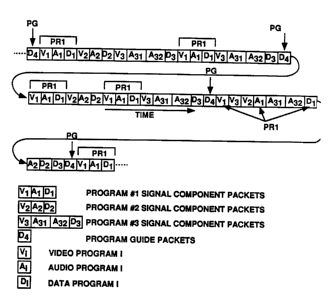
FIGURE 1 shows a signal stream consisting of a string
of boxes which represent signal packets which are components of
a plurality of different television or interactive television
programs. These program components are assumed to be formed
21~59 04 RCA 87,076
-3 -
of compressed data and as such the quantity of video data for
respective images is variable. The packets are of fixed length.
Packets with letters having like subscripts represent components
of a single program. For example, Vj, Ai, Di represent video, audio
5 and data packets and packets designated Vl, Al, Dl, represent
video, audio and data for program 1, and V3, A31, A32, D3,
represent video, audio 1, audio 2 and data components of program
3. In the upper line of the string of packets the respective
components of a particular program are shown grouped together.
10 However there is no necessity of packets from the same program
being grouped as is indicated by the packet sequence shown in
the middle of portion of the string of packets. Nor is there any
particular order for the sequence of occurrence of respective
components .
The string of packets shown in FIGURE 1 represents
three time division multiplexed programs, program 1, PRl, and
programs 2 and 3, plus packets representing a program guide
(packets D4). The program guide includes data which interrelates
program components. The respective program components are
2 0 assigned identifiers substantially independent of the program, and
each component has a different identifier, SCID. For example
SCID's assigned to the video, audio and data packets of program 2
may be 101111000110, 001101000111, and 101010101010
respectively.
2 5 The respective packets are arranged to include a
prefix and a payload as shown in FIGURE 2. The prefix of this
example includes two 8-bit bytes comprising five fields, four (P,
BB, CF, CS) of which are l-bit fields, and one (SCID) of which is a
12-bit field. For purposes of this description, only fields CF, CS
3 0 and SCID are of interest. The SCID field is of course the signal
component identifier. The field CF contains a flag to indicate
whether the payload of the packet is scrambled, and the field CS
contains a flag which indicates which of two alternative
unscrambling keys is to be utilized to unscramble scrambled
packets. The prefix of every packet is packet aligned, thus the
location of the respective fields are easily identifiable.
FIGURE 3 illustrates the packet detector as it relates to
various elements of a digital television receiver. Signal is detected
21~9~4
RCA 87,076
-- 4 --
by an antenna 10 and applied to a tuner detector, 11, which
extracts a particular frequency band of received signals, and
provides baseband signal in a binary format. The frequency band
is selected by the user through a microprocessor 19 by
5 conventional methods. Nominally broadcast digital signals will
have been error encoded using, for example, Reed-Solomon
forward error correcting (FEC) coding. The baseband signals will
thus be applied to a FEC decoder, 12. The FEC decoder 12 will
synchronize the received video and provide a stream of signal
10 packets of the type illustrated in FIGURE 1. The FEC 12 may
provide packets at regular intervals or on demand, by for example
memory controller 17. In either case a packet framing or
synchronizing signal is provided by the FEC circuit, which
indicates the times that respective packet information is
15 transferred from the FEC 1 2.
The detected frequency band may contain a plurality
of time division multiplexed programs in packet form. To be
useful, only packets from a single program should be passed to
the further circuit elements. However the user has no knowledge
20 of which packets to select. This information is contained in a
program guide, which in itself is a program consisting solely of
data which interrelates program signal components through
SCID's. The program guide is a listing for each program, of the
SCID's for the audio, video, and data components of respective
25 programs. The program guide (packets D4 in FIGURE 1) is
assigned a fixed SCID. When power is applied to the receiver, the
microprocessor 19 loads the SCID associated with the program
guide into one of a bank of similar progr:~mm~ble SCID registers
13. The SCID field of the prefix portion of respective detected
30 packets of signal from the FEC 12 are successively loaded in a
further SCID register 14. The progr~mm~ble registers and the
received SCID register are coupled to respective input ports of a
comparator circuit 15, and the received SCID is compared with
the program guide SCID. If the SCID for a packet matches the
3 5 program guide SCID, the comparator 15 conditions a memory
controller 17 to route that packet to a predetermined location in
the memory 18 for use by the microprocessor. If the received
SCID does not match the program guide SCID, the corresponding
2145904
RCA 87,076
-5 -
packet is simply dumped. The elements 13-15 in effect comprise
a plurality of matched filters.
The microprocessor waits for a progr~mming
command from the user via an interface 20, which is shown as a
computer keyboard but which may be a conventional remote
control, or receiver front panel switches. The user may request to
view a program provided on channel 4 (in the vernacular of
analog TV systems). The microprocessor 19 is programmed to
scan the program guide list that was loaded in the memory 18 for
the respective SCID's of the channel 4 program components, and to
load these SCID's in respective other ones of the programmable
registers of the bank of registers 13 which are associated with
corresponding component signal processing paths.
Received packets of audio, video or data program
components, for a desired program, must ultimately be routed to
the respective audio 23, video 22, or auxiliary data 21, (24) signal
processors respectively. The exemplary system of FIGURE 3, first
routes the respective packets to predetermined memory locations
in the memory 18. Thereafter the respective processors 21-24
2 0 request the component packets from the memory 18. It should be
appreciated that the signal components are compressed and that
decompression devices do not require input data on a continuous
basis. Routing the components through the memory provides a
measure of desired signal throttling.
The audio, video and data packets are loaded into
predetermined memory locations to enable the signal processors
easy access to the component data. In order that the appropriate
packets get loaded in the appropriate memory areas, the
respective SCID comparators must be associated with those
3 0 memory areas. This association may be hardwired in the memory
controller 17, or the association may be progr~mm~ble. If the
former, specific ones of the progr~mm~ble registers will always be
assigned the audio, video and data SCID's respectively. If the
latter the audio, video and data SCID's may be loaded in any of the
3 5 programmable registers, and the appropriate association be
programmed in the memory control 17 when the respective SCID's
are loaded in the programmable registers.
2145904
RCA 87,076
-6 -
In the steady state, after the program SCID's have
been stored in the progr~mm~ble registers 13, the SCID's of
received signal packets are compared with all of the SCID's in the
progr~mm~ble SCID registers. If a match is made with either a
5 stored audio, video or data SCID, the corresponding packet
payload will be stored in the audio, video or data memory area
respectively.
The respective signal packets are coupled from the FEC
12 to the memory controller 17 via a signal decryptor 16. Only
10 the signal payloads are scrambled. Whether or not the packet is
to be descrambled is determined by the CF flag in the packet
prefix, and how it is to be descrambled is determined by the CS
flag. If no SCID match is had for a respective packet, the
decryptor may simply be disabled from passing any data.
15 Alternatively, if there is no SCID match for a packet the decryptor
may be allowed to decrypt according to its last settings and the
memory write control may be disabled to dump the respective
packet.
FIGURE 4 illustrates exemplary register-comparator
20 circuitry which may be used for the elements 13-15 in FIGURE 3.
FIGURE 4 includes a plurality of similar register comparator
circuits 36A-36E. Each of these circuits includes a 13-bit parallel-
output register 37 into which is loaded one of the component
SCID's from the microprocessor 19. The parallel output
2 5 connections are respectively coupled to respective first input
connections of a plurality of 13 two-input exclusive NOR circuits,
XNOR's 38-41. A further register, which in this example is a 12-
bit serial-input-parallel-output register 35, is successively loaded
with the 12-bit SCID of the current signal component packet. The
3 0 output connections of this register are respectively coupled to the
second input connections of bit-corresponding 12 XNOR gates of all
of the circuits 36A-36E. The second input connection of the 13th
XNOR gate is coupled to ground potential and its utility will be
discussed below. Each of the circuits 36A-36E includes a
3 5 13-input AND circuit to which the output connections of the 13
XNOR gates are coupled. Whenever the SCID loaded into register
35 matches the SCID programmed into one of the registers of
~ 1 1 5 9 0 ~ RCA 87,076
-- 7 --
circuits 36A-36E, the AND gate of the corresponding circuit will
exhibit a low to high transition indicating the match.
The output connections of the respective AND gates
are coupled to the set input connection of a set-reset flip-flop, 44,
which is edge triggered. The reset input of the flip-flop 44 is
coupled to the packet framing pulse. The packet framing pulse, in
this example, is assumed to be a pulse which goes from logic low
to logic high at the beginning of a packet, and stays at a logic high
for the duration of the packet. The respective flip-flops are
therefore reset to a logic low at the beginning of each packet, and
will thereafter be set to a logic high by a transition of the
associated AND gate going from a logic low to a logic high, when a
match is detected. The packets are assumed to be in bit-serial
format, in this example, and respective bits of the packet are
clocked out of the FEC 12 by a bit clock. A match can occur only
after a SCID is loaded into the register 35, which occurs 16 bit-
clock periods after the leading transition of the packet framing
pulse.
The packet SCID's are clocked into the register 35 by
the bit-clock which is applied to the register 35 through an AND
gate 47. The AND gate 47 is enabled to pass the bit-clock only
during the interval that the SCID occurs in the packet bit stream.
The enable pulse is generated by an edge triggered set-reset flip-
flop 48 which is set by a replica of the packet framing signal that
is delayed by four bit-clock periods and is reset by a further
replica of the packet framing signal that is delayed by sixteen bit-
clock periods. The flip-flop 48 outputs an enable signal which is
12-bit clock periods in duration and occurs four bit-clock periods
after the beginning of the respective packets.
3 0 Similar circuitry may be arranged to load byte serial
signals into a current SCID register if data provided by the FEC
(for an alternative system) is byte serial. Those skilled in the art
of digital circuitry will readily be able to accommodate the
comparator circuitry to the input signal format.
FIGURE 5 shows exemplary decryption apparatus
which may be implemented for the decryptor 16 of FIGURE 3.
The signal packets are decrypted by a conventional decryptor, 79,
which is conditioned to perform descrambling according to
` 21~590~
RCA 87,076
-8 -
descrambling words applied to a descrample word input, DWI.
The packets are applied to the decryptor, 79. via an AND gate, 73,
which is enabled 16 bit-clock periods after the leading transition
of the packet framing pulse. Enabling the AND gate in this
5 manner excises the packet prefix, which has no further use.
The AND gate 73 is also enabled by an OR circuit 72
which is responsive to the SCID detector 15. If any one of the
programmed SCID's is matched, the OR 72 provides an enabling
signal which allows the packet payload to enter the decryptor. If
1 0 there is no SCID match, the AND gate 73 in effect dumps the
current packet of data.
The scramble flags CF and CS are clocked and stored in
a register 75. The CF flag is coupled to an enable input connection
EN of the decryptor. Responsive to the flag exhibiting a logic one
1 5 level, the decryptor is conditioned to pass the signal from the FEC
unaltered. That is no descrambling is performed. Alternatively if
the CF flag exhibits a logic low level, descrambling is performed
by the decryptor.
Each program component may have two unique
2 0 descrambling codes. These descrambling codes are stored in two
sets of decryption registers 76A and 76B. The registers 76A have
respective output connections coupled to a multiplexor 77A, and
the registers 76B have respective output connections coupled to a
multiplexor 77B. The multiplexors 77A and 77B have respective
2 5 output connections coupled to a two-to-one multiplexor 78. The
multiplexor 78 has a control electrode coupled to be responsive to
the control flag CS in the register 75. If the flag CS is a logic high
or logic low the decryption key is selected from a register in bank
76A or 76B respectively. The multiplexors 77A and 77B are
3 0 controlled by the SCID detector output signal to select the
decryption key register in the bands 76A and 76B associated with
the current packet output by the FEC 12.
The registers 76A and 76B may be loaded with fixed
decryption key values. However to provide scrambling flexibility,
3 5 the preferred embodiment provides for registers 76A and 76B
which may be programmed with decryption keys either from the
microprocessor 19 or a smart card interface (not shown).
21~9~4
RCA 87,076
g
FIGURE 6 illustrates exemplary apparatus for the
memory controller 17 shown in FIGURE 3. This figure is included
to illustrate elements which are interrelated to progr~mming the
registers 13 in FIGURE 3. Each program component is stored in a
different contiguous block of the memory 18. In addition other
data, such as data generated by the microprocessor 19 or a Smart
Card (not shown) may be stored in the memory 18.
Memory addresses are applied by a multiplexor 105,
and memory input data is applied by a multiplexor 99. Output
data is provided by a further multiplexor 104. Output data
provided by the multiplexor 104 is derived from the multiplexor
19, the memory 18 or directly from the multiplexor 99. Program
data is presumed to be of standard picture resolution and quality,
and occurring at a particular data rate. On the other hand high
definition television signals, HDTV, occur at a significantly higher
data rate. Practically all data provided by the FEC will be routed
through the memory 18 via the multiplexor 99, except for the
higher rate HDTV signals which may be routed directly to the
multiplexor 1 04.
2 0 Memory addresses are provided to the multiplexor
105, from program addressing circuitry 79-97, from the
microprocessor 19, from the Smart Card apparatus and possibly
from other auxiliary devices. Selection of the particular address
at any particular time period is controlled by a direct memory
access DMA, circuit 98. The SCID control signals and "data needed"
signals from respective signal processors are applied to the DMA
98, and responsive thereto, memory access contention is
arbitrated. The DMA 98 cooperates with a Service Pointer
Controller 93, to provide the appropriate read or write addresses
3 0 for respective program signal components.
The respective addresses for the various signal
component memory blocks are generated by four groups of
program component or service pointer registers 83, 87, 88, and
92. The starting pointers for respective blocks of memory, into
3 5 which respective signal components are stored, are contained in
registers 87 for the respective signal components. The start
pointers may be fixed values, or they may be calculated by
21~90~
RCA 87,076
- 1 0 -
conventional memory management methods in the microprocessor
19.
The last address pointers for respective blocks are
stored in the bank of service registers 88, one for each potential
5 program component. Similar to the start addresses, the end
addresses may be fixed values or they may be calculated values
provided by the microprocessor l 9. Using calculated values for
starting and end pointers is preferred because it provides a more
versatile system with less memory.
1 0 The memory write pointers or head pointers are
generated by the adder 80 and the service head registers 83.
There is a service head register for each potential program
component. A write or head pointer value is stored in a register
83, and provided to an address multiplexor 105 during a memory
1 5 write cycle. The head pointer is also coupled to the adder 80,
wherein it is incremented by one unit, and the incremented
pointer is stored in the appropriate register 83 for the next write
cycle. The registers 83 are selected by the service pointer
controller, 93, for the appropriate program component currently
2 0 being serviced.
In this example it is assumed that the start and end
pointers are 16-bit pointers. The registers 83 provides 16 bit
write or head pointers. The memory 18, on the other hand has
18-bit addresses. The 18-bit write addresses are formed by
2 5 concatenating the two most significant bits of the start pointers to
the 16-bit head pointers, with the start pointer bits in the most
significant bit positions of the combined 18-bit write address. The
start pointers are provided by the respective registers 87 to the
service pointer controller 93. The service pointer controller
parses the more significant start pointer bits from the start
pointers stored in registers 87, and associates these bits with the
16-bit head pointer bus. This is illustrated by the bus 96 shown
being combined with the head pointer bus exiting the multiplexor
85.
3 5 Similarly, memory read pointers or tail pointers are
generated by the adder 79 and the service tail registers 92. There
is a service tail register for each potential program component. A
read or tail pointer value is stored in a register 92, and provided
21459~
RCA 87,076
-1 1-
to the address multiplexor 105 during a memory read cycle. The
tail pointer is also coupled to the adder 79, wherein it is
incremented by one unit, and the incremented pointer is stored in
the appropriate register 92 for the next read cycle. The registers
5 92 are selected by the service pointer controller, 93, for the
appropriate program component currently being serviced.
The registers 92 provides 16 bit tail pointers. 1 8-bit
read addresses are formed by concatenating the two most
significant bits of the start pointers to- the 16-bit tail pointers,
10 with the start pointer bits in the most significant bit positions of
the combined 1 8-bit write address. The service pointer controller
parses the more significant start pointer bits from the start
pointers stored in registers 87, and associates these bits with the
1 6-bit tail pointer bus. This is illustrated by the bus 94 shown
15 being combined with the tail pointer bus exiting the multiplexor
90.
Data is stored in the memory 18 at the calculated
address. After storing a byte of data, the head pointer is
incremented by one and compared to the end pointer for this
2 0 program component, and if they are equal the more significant
bits of the head pointer are replaced with the lower 14 bits of the
start pointer and zeros are placed in the lower two bit positions of
the head pointer portion of the address. This operation is
illustrated by the arrow 97 pointing from the service pointer
2 5 controller 93 to the head pointer bus from the multiplexor 82. It
is presumed that application of the lower 14 start pointer bits
override the head pointer bits. Replacing the head pointer bits
with the lower start pointer bits in the address causes the
memory to scroll through the memory block designated by the
3 0 upper two start pointer bits, thus obviating reprogr~mming write
addresses at the start of each packet to a unique memory location
within a block.
For the case in which the head pointer is now equal to
the tail pointer (used to indicate where to read data from the
3 5 memory 18) a signal is sent to the interrupt section of the
microprocessor to indicate that a head tail crash has occurred.
Further writing to the memory 18 from this program channel is
214S90~
RCA 87,076
- -1 2-
disabled until the microprocessor re-enables the channel. This
case is very rare and should not occur in normal operation.
Data is retrieved from the memory 18 at the request
of the respective signal processors at addresses calculated by the
5 adder 79 and registers 92. After reading a byte of stored data,
the data the tail pointer is incremented by one and compared to
the end pointer for this logical channel in the service pointer
controller 93. If the tail and end pointers are equal then the tail
pointer is replaced with the lower 14 bits of the start pointer and
10 zeros in the lower two bits. This is illustrated by the arrow 95
em~n~ting from controller 93 and pointing to the tail pointer bus
from the multiplexor 90. If the tail pointer is now equal to the
head pointer then the respective memory block is defined as
empty and no more bytes will be sent to the associated signal
15 processor until more data is received from the FEC for this
program channel.
Memory read/write control is performed by the
service pointer controller and direct memory access, DMA,
elements 93 and 94. The DMA is programmed to schedule read
2 0 and write cycles. Scheduling is dependent upon whether the FEC
12 iS providing data to be written to memory or not. FEC data
write operations take precedence. In the exemplary apparatus
illustrated in FIGURE 6, there are four types of apparatus which
may access the memory. These are Smart Card (not shown), the
2 5 FEC 12 (more precisely the decryptor 16), the microprocessor 19
and one of the application devices such as the audio and video
processors. Memory contention is handled in the following
manner. The DMA, responsive to data requests from the various
processing elements listed above allocates memory access as
3 0 follows. Access to the memory is provided in 95 nS time slots
during which a byte of data is read from or written to the
memory 18. There are two major modes of access allocation,
defined by the FEC Providing Data, or the FEC Not Providing Data
respectively. For each of these modes the time slots are allocated
3 5 as follows, assuming a maximum FEC data rate of S
Mbytes/second, or one byte for each 200 nS. These are:
FEC Providing Data
1) FEC data write;
21~S90~
RCA 87,076
- 1 3 -
2) Application device read/Microprocessor read/write;
3) FEC data write;
4) Microprocessor read/write;
and for
S FEC Not Providing Data
1 ) Smart Card read/write;
2) Application device read/Microprocessor read/write;
3 )Smart Card read/write;
4) Microprocessor read/write.
Because FEC data writes cannot be deferred, the FEC (or more
correctly the decryptor), when providing data must be guaranteed
memory access during each 200 nS interval. Alternate time slots
are shared by the application devices and the microprocessor.
When there is no data available for the requesting devices, the
microprocessor is provided use of the application time slots.
The Controller 93 communicates with the SCID
detector to determine which of the respective Start, head and end
pointer registers to access for memory write operations. The
controller 93 communicates with the DMA to determine which of
2 0 the start, end and tail registers to access for memory read
operations. The DMA 98 controls selection of the corresponding
addresses and data by the multiplexors 99, 104 and 105.
Consider that it is desired to reprogram one of the
SCID registers 13 without changing the rem~ining SCID registers.
This may occur, for example, when it is desired to change to a
different one of multiple audio components, without interfering
with processing of the other signal components. This activity
requires changing pointers in respective ones of the registers 83,
87, 88 and 92, as well as allocating memory space etc., all of which
3 0 requires finite time. Since reprogr~mming cannot be performed
instantaneously, if reprogr~mming is not carried out in a
prescribed sequence, there is a high probability that undesired
data provided by the FEC may encroach one of the signal
processors and cause a system "crash".
3 5 The preferred reprogr~mming sequence is performed
as follows. When a program component is to be de-selected by
removing its SCID from one of the registers 13, the microprocessor
is programmed to test the SCID detector output control bus to
2145~0~
RCA 87,076
- 1 4-
determine if that channel is currently active, i.e., it is currently
processing that program component packet. If it is active the
system waits until that service of the SCID detector output goes
inactive. After that program component goes inactive the four
5 most significant bits of the new SCID are loaded into the
appropriate register. In addition a logic high toggle bit is loaded
into the TB-bit position of the register, see FIGURE 4. The toggle
bit is applied to the 13th XNOR gate and is a different logic level
than the other input connection of the 13th XNOR. This insures
1 0 that the AND gate 42 is disabled and consequently, that particular
program service or channel is inactivated. (Note all 12 bits are
not simultaneously loaded into the register 37 in this example
because the load data bus is considered to be only 8-bits wide.)
In addition the memory management circuitry has as yet not been
1 5 reconfigured to accommodate the SCID change. Therefore, before
loading the LSB's of the SCID into the register 37, the memory
management circuits are reconfigured under control of the
microprocessor 19, and then the eight LSB's of the SCID are loaded
into register 37, after which the toggle bit is set low to reactivate
2 0 that program channel or service.
The inventors have found that it is particularly
prudent to prioritize the SCID control signals. It is possible, and
sometimes desirable, that the same SCID is loaded in more than
one SCID register. It then becomes necessary to insure that the
2 5 system can accommodate the simultaneous detection of the SCID
by two or more detectors. The respective SCID are prioritized
according to a hierarchy established by the system designer. In
the current example the respective detectors 36A- 36E are
prioritized in that order. Thus if a SCID is detected by detector
3 0 36A and others of detectors 36B-36E, an output control signal will
be provided by detector 36A but the output control signals for all
other detectors 36B-36E will be inhibited. Alternatively, if
detector 36A does not detect the current SCID but detector 36B,
and other ones of the detectors 36C-36E do detect the current
3 5 SCID, a control signal will be provided for detector 36B while the
output of detectors 36C-36E are inhibited. Similarly if detector
36C is the highest ordered detector in the hierarchy set forth
` 214590~
RCA 87,076
- 1 5 -
above, to detect the current SCID, the output signals of detectors
36D-36E will be inhibited and so forth.
Output control signal prioritization is performed by the
circuit element 51 of FIGURE 4. Exemplary circuitry to perform
5 this function is illustrated in FIGURE 7. This is a familiar
thermometer decoder and need not be described in detail.
1 0