Note: Descriptions are shown in the official language in which they were submitted.
CA 0214~918 1997-04-29
FEEDFORWARD AMPLIFIER
WITH REDUCED DISTORTION IN WIDE BAND
The present invention relates to a feedforward
amplifier and, in particular, to a feedforward amplifier for
detecting and suppressing distortion in an output signal
amplified by a feedforward loop.
As a linear amplifier employed to simultaneously
amplify many frequencies in a high-frequency band, there has
been known a feedforward amplifier described in the Japanese
Patent Laid-Open Hei-1-198809. Figure 1 shows an example of
the structure of the conventional feedforward amplifier. The
configuration includes a distortion sensing loop A and a
distortion removing loop B, such that multiple frequencies of
an input signal received from an input terminal 101 are
amplified simultaneously by a main amplifier 104. The sensor
loop A cancels input signal components to achieve an
amplification in which non-linear distortion components
caused by the amplification are detected. The remover loop
B amplifies the detected distortion components by an
auxiliary amplifier 115, and adds the resultant signal to an
output signal from the main amplifier 104, thereby cancelling
the distortion components.
The distortion sensor loop A includes a pilot
oscillator 118, a (directional) coupler 119 for superimposing
a pilot signal onto an input signal, a two-output distributor
102, a vector adjuster 103 for adjusting attenuation and
phase shift, a main amplifier 104, a delay line 106, a
coupler 110, a detector (DET) 122, and a controller 109.
Additionally, couplers 107 and 108 are arranged as shared
components for the sensor loop A and remover loop B. The
coupler 108 produces an output signal, which is fed via the
coupler 110 to the detector 122 to be detected therein. The
detected signal is applied to the controller 109. The
controller 109 supervises the vector adjuster 103 to set the
output level of the detector 122 to a minimum value.
Furthermore, the distortion remover loop B includes
~,
, - -- 1 --
CA 0214~918 1997-04-29
the couplers 107 and 108, which are also used by the
distortion sensor loop A, a pilot oscillator 120, a coupler
121, a delay line 111, a coupler 112, a vector adjuster 113
for regulating attenuation and phase shift, an auxiliary
amplifier 115, a coupler 116, a detector (DET) 123, and a
controller 114.
In the output circuit of the feedforward circuit, the
controller 114 detects the pilot signal via the coupler 116
and detector 123 to control the vector adjuster 113 so as to
set the sense level of the pilot signal to a minimum value.
Description will now be given of operation of the
conventional linear (feedforward) amplifier constructed as
above. A multiplex signal containing many frequencies in a
high-frequency band is received via the input terminal 101 to
be superimposed by the coupler 119 onto the output signal
from the pilot oscillator 118. The obtained signal is
distributed by the distributor 102 as a first signal and a
second signal.
The first signal is fed to the vector adjuster 103.
Attenuation and phase shift thereof are regulated by the
adjuster 103. The resultant signal is delivered to and
amplified by the main amplifier 104, and coupled by the
coupler 121 with the pilot signal generated from the pilot
oscillator 120. The obtained signal is fed via the coupler
107 and delay line 111 to the coupler 112. The signal fed to
the coupler 112 is called a main amplification signal
including distortion components caused during the
amplification by the main amplifier 104.
The second signal thus distributed by the distributor
102 is delayed through the delay line 106 by a delay time
equivalent to that of the vector adjuster 103 and main
amplifier 104, and fed to the coupler 108. On the other
hand, a portion of the main amplification signal is branched
by the coupler 107 to be supplied to the coupler 108 in an
inverse-phase state. These signals are mixed with each other
by the coupler 108, and supplied to the coupler 110. The
pilot signal contained in the portion of the signal branched
r
CA 0214~918 1997-04-29
by the coupler 110 is detected by the detector 122, and input
to the controller 109. The controller 109 adjusts
attenuation and phase shift of the vector adjuster 103 to
minimize the output signal level of the detector 122.
In the construction, the output terminal of the
distributor 102 is linked with the coupler 108 only by the
delay line 106, and hence distortion generated by the line
106 is negligible. Consequently, if the sensor loop A is
appropriately operating, the portion of the input signal
passed through and amplified by the vector adjuster 103 and
main amplifier 104 is coupled by the coupler 108 with the
first signal in an inverse-phase state. In the result, only
the distortion components generated or mixed in the main
amplifier 104 are output from the coupler 108.
The distortion component signal fed from the coupler
108 to the coupler 110 is then delivered to the vector
adjuster 113 for adjustment of attenuation and phase shift
thereof. The obtained signal is then supplied to and
amplified by the auxiliary amplifier 115. The amplified
distortion component is then mixed by the coupler 112 in the
reverse-phase state with the main amplification signal
delayed through the delay line 111 by a propagation delay
time equal to the delay through the vector adjuster 113 and
auxiliary amplifier 115.
The composite signal is then supplied to the coupler
116 such that a portion thereof is branched to the detector
123. The detector 123 conducts, for example, a simultaneous
detection for the input composite signal to extract therefrom
a pilot signal, and then sends the pilot signal to the
controller 114. The controller 114 regulates attenuation and
phase shift of the vector adjuster 113 to set the output
level of the detector 123 to a minimum value. As a result,
in the main amplification signal sent from the coupler 116 to
the output terminal 117, the pilot signal takes the minimum
value, namely, the distortion component is minimized.
The signal fed to the input terminal 101 is subjected
to modulation due to information transmission, and may
CA 0214~918 1997-04-29
possibly be continually interrupted in some cases.
Consequently, when the input signal is adopted to control
amplification, the amplified signal becomes unstable.
However, according to the conventional linear (feedforward)
amplifier configured as above, since amplification is
supervised by a pilot signal of which the level and frequency
are determined, there can be attained a stable amplification
signal.
However, in the linear amplifier of the prior art, to
obtain compression of, for example, at least 30 decibel (dB)
in a frequency band, it has been shown in computation that
the deviations of amplitude and phase are required to be
within +0.3dB and +2~, respectively. These values indicate
deviations respectively thereof related to the frequency used
and the frequency of the pilot signal when the pilot signal
is completely cancelled. Consequently, in the conventional
amplifier, a stable control operation is expected in the
neighbourhood of the frequency of the pilot signal. However,
to remove the 3OdB distortion uniformly in any zone of a
frequency band, the constituent elements of the loops
included in the main and auxiliary amplifiers 104 and 115 are
required to have severe frequency characteristics, namely,
the deviations of amplitude and phase are required to be
within +0.3dB and +2~, respectively.
In consequence, the linear amplifier of the prior art
is attended with a problem that the amplifier is unsuitable
for amplification of signals in a wide band.
It is therefore an object of the present invention to
provide a linear amplifier capable of producing a stable
amplification signal with a compressed distortion in a wide
band.
In accordance with the present invention, there is
provided a feedforward amplifier including a main amplifier
circuit including first equalizing means for adjusting
frequency characteristics of amplitude and phase of an input
signal thereto and first amplifying means for amplifying the
input signal, the first equalizing means and the first
CA 0214~918 1997-04-29
amplifying means being arranged in a cascade connection, the
main amplifier circuit producing therefrom an amplification
signal by amplifying the input signal; an auxiliary amplifier
circuit including distortion sensing means for branching a
portion of the amplification signal, mixing the signal
portion with the input signal, and sensing a distortion
signal appearing in the amplification signal, second
equalizing means for adjusting frequency characteristics of
amplitude and phase of the distortion signal, and second
amplifying means for amplifying the distortion signal sensed
by the sensing means; the distortion sensing means, the
second equalizing means, and the second amplifying means
being disposed in a cascade connection, the auxiliary
amplifying means outputting the amplified distortion signal
therefrom; and distortion removing means for removing the
distortion signal according to the amplification signal and
the amplified distortion signal.
A feedforward amplifier in accordance with the present
invention includes oscillator means for generating an
oscillation signal having a predetermined frequency, first
coupling means for superimposing the oscillation signal onto
an input signal and outputting a superimposed signal,
distributor means for distributing the superimposed signal as
a first signal and a second signal respectively to two
destinations, equalizing means for adjusting frequency
characteristics of amplitude and phase of the first signal,
amplifying means for amplifying an output signal from the
equalizing means, second coupling means for coupling the
second signal in a reverse-phase state with an output signal
from the amplifying means, sensing means for sensing in an
output signal from the second coupling means the oscillation
signal superimposed by the first coupling means, and control
means for adjusting frequency characteristics of amplitude
and phase of the equalizing means according to a sense signal
sensed by the sensing means.
A feedforward amplifier in accordance with the present
invention includes first oscillator means for generating a
~ - 5 -
CA 0214~918 1997-04-29
first oscillation signal having a predetermined frequency,
first coupling means for superimposing the first oscillation
signal onto an input signal and outputting a superimposed
signal, distributor means for distributing the superimposed
signal as a first signal and a second signal respectively to
two destinations, first equalizing means for adjusting
frequency characteristics of amplitude and phase of the first
signal, first amplifying means for amplifying an output
signal from the first equalizing means, second oscillator
means for generating a second oscillation signal having a
predetermined frequency, second coupling means for coupling
the second signal with an output signal from the first
amplifying means, thereby producing a superimposed
amplification signal, third coupling means for branching and
extracting a portion of an output signal from the second
coupling means, fourth coupling means for coupling an output
signal from the third coupling means in a reverse-phase state
with the second signal distributed by the distributor means,
second equalizing means for adjusting frequency
characteristics of amplitude and phase of an output signal
from the fourth coupling means, second amplifying means for
amplifying an output signal from the second equalizer means,
fifth coupling means for coupling an output signal from the
second coupling means in a reverse-phase state with the
superimposed amplification signal, first sensing means for
sensing from an output signal from the fourth coupling means
the first oscillation signal superimposed by the first
coupling means, first control means for adjusting frequency
characteristics of amplitude and phase of the first equalizer
means according to a sense signal sensed by the first sensing
means, second sensing means for sensing from an output signal
from the fifth coupling means the second oscillation signal
superimposed by the second coupling means, and second control
means for adjusting frequency characteristics of amplitude
and phase of the second equalizing means according to a sense
signal sensed by the second sensing means.
A feedforward amplifier in accordance with the present
CA 0214~918 1997-04-29
invention further includes first delay means between the
third and fifth coupling means, the first delay means having
a delay time equivalent to a time constant of signal delay of
the second equalizer means and the second amplifying means
and second delay means at an upstream position preceding the
fourth coupling means, the second delay means having a delay
time equivalent to a time constant of signal delay of the
first equalizer means and the first amplifying means.
In accordance with the feedforward amplifier of the
present invention, the frequency characteristics of the
amplitude and phase of the input signal are adjusted and
amplified to obtain an amplification signal. A portion of
the signal is used as an input signal to be mixed with the
input signal so as to generate a composite signal, thereby
detecting a distortion signal caused in the amplification
signal. The frequency characteristics of the amplitude and
phase of the detected distortion signal are adjusted and
amplified to attain an amplified distortion ,signal.
Consequently, the distortion signal appearing in the
amplification signal can be removed by the distortion
removing means according to the amplified distortion signal.
The objects and features of the present invention will
become more apparent from a consideration of the following
detailed description taken in conjunction with the
accompanying drawings, in which:
Figure 1 is a schematic diagram showing an example of
the circuit configuration of a conventional feedforward
amplifier;
Figure 2 is a diagram showing the circuit
configuration of a feedforward amplifier in accordance with
the present invention;
Figure 3 is a diagram schematically showing the
circuit configuration of a first embodiment of an equalizer
constituting the feedforward amplifier of Figure 2;
Figure 4 is a diagram showing the circuit
configuration of a second embodiment of the equalizer in the
feedforward amplifier of Figure 2;
-- 7
CA 0214~918 1997-04-29
Figure 5 is a graph showing an example of frequency
characteristics of components constituting the equalizer of
Figure 4; and,
Figure 6 is a flowchart showing an example of the
adjusting procedure of the equalizer shown in Figure 4.
Referring now to the accompanying drawings,
description will be given in detail of an embodiment of the
feedforward amplifier in accordance with the present
invention. Figures 2 to 5 show an embodiment of the
feedforward amplifier in accordance with the present
invention.
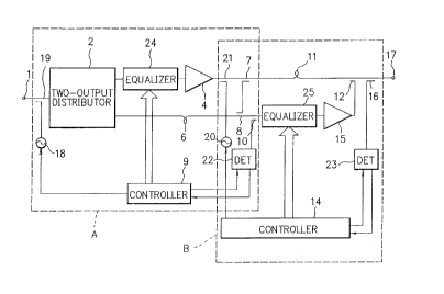
Circuit configuration
Figure 2 shows the circuit construction of the
embodiment in accordance with the present invention. The
feedforward amplifier includes common elements with the
conventional feedforward amplifier. That is, the amplifier
includes a distortion sensing loop A in which multiple
frequencies contained in a multiplex signal in a high-
frequency band are received via the input terminal 1 to be
simultaneously amplified, and in which input signal
components are cancelled to allow sensing of non-linear
distortion components caused during amplification, and a
distortion removing loop B in which the sensed distortion
components are amplified by the auxiliary amplifier 15 before
being added to an output signal from the main amplifier 4 so
as to cancel its distortion components.
The distortion sensor loop A includes a coupler 19,
a pilot oscillator 18, a two-output distributor 2, an
equalizer 24 for regulating frequency characteristics of
attenuation and delay, a main amplifier 4, a delay line 6,
and a controller 9. In addition, (bi-directional) couplers
7 and 8 are arranged therein to be commonly used also by the
distortion removing loop B.
The pilot oscillator 18 is an oscillator which
generates and outputs therefrom a signal having a
predetermined frequency. The oscillation frequency is
- 8 -
CA 0214~918 1997-04-29
supervised by a control signal from the controller 9. The
coupler 19 mixes the multiplex signal received via the input
terminal 1 with the output signal from the pilot oscillator
18. The distributor 2 distributes an output signal from the
coupler 19 to two destinations.
The equalizer 24 adjusts frequency characteristics of
attenuation and phase shift of a first signal distributed
from the distributor 2 according to an output signal from the
controller 9. Examples of constitution of the equalizer 24
are shown in Figures 3 and 4. The contents thereof will be
described later in this specification.
In the equalizers 24a and 24b respectively shown in
Figures 3 and 4, signal components of signals supplied to
input terminals 46 and 56 are significantly regulated
according to magnitude of a control voltage applied to
control signal input terminals 481 ~ 488 and 581 ~ 584, thereby
delivering regulated signals to respective output terminals
47 and 57.
The main amplifier 4 amplifies a signal outputted from
the equalizer 24. The controller 9 receives as an input
thereto an output signal from the detector 22 to output
control signals respectively to the pilot oscillator 18 and
equalizer 24.
The coupler 21, shared between the sensing and
removing loops A and B, superimposes the pilot signal from
the pilot oscillator 20 onto an output signal from the main
amplifier 4. Each of the couplers 7 and 10 branches and
extracts a portion of a signal inputted thereto, whereas the
coupler 8 mixes the signal branched by the coupler 7 in an
inverse-phase state. The detector (DET) 22 separates and
extracts the pilot signal from the signal branched by the
coupler 10.
The distortion removing loop B includes a delay line
11 for delaying a signal, couplers 12 and 16 for separating
and/or coupling signals, an equalizer 25, a controller 14 for
supervising the pilot oscillator 20 and equalizer 25, an
auxiliary amplifier 15, a detector 23, and the common
CA 0214~918 1997-04-29
couplers 7, 8, lO and 21, the pilot oscillator 20, and the
detector 22 which are also used by the distortion sensor
loop.
Figure 3 shows a firstly-constituted example of the
equalizer 24. In the equalizer 24a of Figure 3, between
output terminals of an 8-output distributor 4l and input
terminals of an 8-input mixer 44, delay lines 421 to 428 and
variable attenuators 431 to 438 are respectively connected in
series. The distributor 4l has an input section connected to
the input terminal 46, whereas the mixer 44 possesses an
output section linked with the output terminal 47. The
attenuators 431 to 438 respectively include control signal
sections respectively coupled with the control signal input
terminals 481 to 488.
The 8-output distributor 4l receives one signal via
the input terminal to distribute the signal to eight output
ports. The delay line 42 includes delay lines 421 to 428 each
with a mutually-different time constant. The variable
attenuators 431 to 438 receive input signals through the
respective delay lines 421 to 428 to produce therefrom signals
attenuated according to respective control signals from the
control signal input terminals 481 to 488. The 8-input mixer
mixes eight output signals from the attenuators 421 to 428
into one mixed signal to be output to the output terminal 47.
Figure 4 shows an example of the secondly-constituted
embodiment of the equalizer 24. In the configuration of the
equalizer 24b of Figure 4, a variable attenuator 51 dominant
in a high-frequency range, a variable phase shifter 52
dominant in a high-frequency range, a variable attenuator 53
dominant in a low-frequency range, and a variable phase
shifter 54 dominant in a low-frequency range are arranged in
a cascade connection.
Figure 5 shows characteristics of constituent
components of the equalizer 24b of Figure 4. Graphs 61 to 64
shown in Figure 5 represent examples of characteristics in
which respective control signals applied to the control
signal input terminals 581 to 584 are employed as parameters.
-- 10 --
c~
CA 0214~918 1997-04-29
A multiplex signal including many frequencies in a
high-frequency band is supplied to the input terminal 1 to be
then mixed by the coupler 19 with an output signal from the
pilot oscillator 18. The mixed signal is distributed as two
signals including a first signal and a second signal from the
distributor 2. The first signal is fed to the equalizer 24
to be subjected to adjustment of attenuation and phase shift
thereof, and then the obtained signal is supplied to and
amplified by the main amplifier 4. The amplified signal is
superimposed by the coupler 21 onto a pilot signal created
from the pilot oscillator 20, to be delivered via the coupler
7 and delay line 11 to the coupler 12. The input signal to
the coupler 12 is the main amplification signal containing
distortion components caused during amplification in the main
amplifier 4.
The second signal from the distributor 2 is delayed
through the delay line 6 by a delay time equivalent to the
signal delay time related to the equalizer 24 and main
amplifier 4. The obtained signal is coupled in the reverse-
phase state by the coupler 8 with a portion of the mainamplification signal branched by the coupler 7. The
composite signal is delivered to the coupler 10. A portion
of the input signal is branched by the coupler 10 to the
detector 22. The pilot signal contained in the input signal
is detected therein and is then fed to the controller 9. The
controller 9 accordingly regulates the equalizer 24 to set
the output signal level of the detector 22 to a minimum
value.
The output terminal of the distributor 2 is linked
with the coupler 8 only by the delay line 6. Logically,
there does not exist any element causing distortion. In
consequence, if the operation of the sensor loop A is
appropriate, only the distortion components mixed with or
generated in the input signal when the input signal is passed
through and amplified by the equalizer 24 and main amplifier
4 (primarily caused by the main amplifier 4) are supplied
from the coupler 8 to the coupler 10.
CA 0214~918 1997-04-29
The distortion components fed to the coupler 10
undergo adjustment of frequency characteristics of
attenuation and phase shift by the equalizer 25. The
adjusted signal is input and amplified by the auxiliary
5amplifier 15 to be output to the coupler 12. The output
signal from the auxiliary amplifier 15 is coupled by the
coupler 12 with the main amplification signal, delayed
through the delay line 11 by a delay time of the equalizer 25
and auxiliary amplifier 15. The composite signal is fed to
10the coupler 16 such that a portion thereof is branched to the
detector 23. The detected signal is then input to the
controller 14.
The detector 23 carries out, for example, a
synchronous detection to extract the pilot signal from the
15input signal, and then delivers the pilot signal to the
controller 14. The controller 14 supervises characteristics
of the equalizer 25 so as to set the output level of the
detector to a minimum value. In the result, the output
terminal 17 is supplied with a main amplification signal in
20which the pilot signal is minimized, namely, the distortion
components take a minimum value.
Referring now to the flowchart of Figure 6, a
description will be given of the adjusting procedures
employed by the sensing and removing loops A and B. In this
25connection, the equalizer 24b of the second embodiment, shown
in Figure 4, will be used as the equalizers 24 and 25.
In step S71, the pilot oscillators 18 and 20 are
activated to oscillate in upper ranges of respective
frequency bands. In step S72, the variable attenuator 51 and
30variable phase shifter 52 of the equalizers 24 and 25 are
adjusted.
In step S73, the pilot oscillators 18 and 20 are
caused to oscillate in lower zones of respective frequency
bands. In step S72, the variable attenuator 53 and variable
35phase shifter 54 of the equalizers 24 and 25 are regulated.
In step S76, a check is made to decide whether or not
the detected level exceeds the preset value. If the level
12 -
CA 0214~918 1997-04-29
exceeds the value (NO is the flowchart), control is returned
to step S72 to repeatedly execute the subsequent steps up to
step S76; otherwise, the adjusting procedure is terminated.
As described above, the equalizer 24b shown in Figure
4 includes a cascade connection of a variable attenuator 51
and a variable phase shifter 52 which are dominant in a high-
frequency range, and a variable attenuator 53 and a variable
phase shifter 54 which are dominant in a low-frequency range.
Consequently, according to the procedures above, the variable
attenuators and phase shifters having dominant
characteristics in the respective frequency bands can be
repeatedly adjusted by sequentially changing the frequency of
the pilot signal, thereby obtaining desired characteristics.
In this operation, oscillation frequencies of the pilot
oscillators 18 and 20 are required to be different from that
of the high-frequency signal supplied to the input terminal
1.
In addition, when the equalizer 24a is employed as the
equalizers 24 and 25, there can be used the ZF method and the
least-mean-square (LMS) method which are used to control
transversal filters.
In addition to the control operation achieved by
altering oscillation frequencies of the pilot oscillators 18
and 20, there may be conducted a similar control operation by
expanding the frequency band of the pilot signal through
achieving a spectrum diffusion modulation for the pilot
signal.
According to the embodiment above, the vector adjuster
conventionally adopted to regulate amplitude and phase is
replaced with an equalizer capable of adjusting frequency
characteristics of amplitude and phase so as to vary
oscillation frequency characteristics of the pilot signal
oscillator. Alternatively, a spectrum diffusion modulation
is carried out for the pilot signal to advantageously
configure a feedforward amplifier having an optimal operating
point in the bands to be used.
Description has been given of an embodiment of the
- 13 -
,
CA 0214~918 1997-04-29
present invention only by way of example. However, the
present invention is not restricted by the embodiment,
namely, the embodiment can be changed or modified within the
scope and spirit of the present invention.
As can be seen from the description above, when a
signal is input to the feedforward amplifier in accordance
with the present invention, frequency characteristics of
amplitude and phase of the signal are adjusted and amplified
to produce an amplification signal. A portion thereof is
branched, allowing a distortion signal to be detected from
the branched signal. Frequency characteristics of amplitude
and phase of the distortion signal are adjusted and amplified
to attain an amplified distortion signal. Since distortion
caused in the amplification signal is removed based on the
amplified distortion signal, there can be produced a
multiplex amplification signal containing multiple
frequencies.
While the present invention has been described with
reference to the particular illustrative embodiments, it is
not to be restricted by those embodiments but only by the
appended claims. It is to be appreciated that those skilled
in the art can change or modify the embodiments without
departing from the scope and spirit of the present invention.
- 14 -