Note: Descriptions are shown in the official language in which they were submitted.
CA 02146339 2000-03-17
WO 94/11791 ,~ ~ ~ ~ ~ ~ ~ PCT/US93/05311
CHARGING ROLLER WITH BLENDED CERAMIC LAYER
The invention relates to charging rollers for use in
xerographic reproduction machines.
In a xerographic copy machine electric charge is applied to
a photoreceptor drum (PRD). An image to be copied is scanned
with a strong light source and then reflected to the
photoreceptor drum. The light dissipates the charge on the PRD
where there is no reflected image. The reflected image, which
is now in the form of patterns of charges on the PRD, attracts
particles of toner. The toner is typically a carbon black
pigment with a thermoplastic binder. The particles of toner are
transferred to the substrate (paper) and bonded to it using heat
and pressure to form the completed copy. In another system, the
charge may be first transferred to the substrate so that the
toner is attracted to the substrate rather than to the PRD.
Depending on the technology of the copying system, both the
electric charge and the toner can be delivered to the proper
location by different means. Electric charge may be applied to
the PRD by a corona charging wire or by a charge transfer
roller.
If the charge is applied with a roller-, the charging,
discharging, and capacitance characteristics of the roller
surface are important factors to the operation of the system.
The charge transfer roller surface is charged to the proper
voltage. Charge is transferred to the PRD. The charge transfer
roller surface is then recharged for the next cycle. Prior to
recharging, it may be discharged to produce a uniform surface
and starting point for the next charging cycle.
Charge transfer rollers typically are coated or covered
with a layer of semiconductive material. Coating materials can
include rubber, thermoplastic, or thermoset compounds containing
carbon black or other low resistance additives, and anodized
1
3
._ _......_.._ ____..
WO 94/11791 , , PCT/US93/05311
~ ~~33~
aluminum with special sealers to give the proper electrical
properties.
The surface layer of the charge transfer roller has both
volume resistance properties and capacitance properties. For
charging and discharging the charge transfer roller surface, the
surface layer functions electrically as an RC series circuit, a
resistor and capacitor in series. The layer therefore has a
time constant, which is a function of the product of the
resistance and capacitance (R*C). For a roller surface layer,
this may be expressed in seconds per unit area (e. g.
microseconds per square millimeter or seconds per square inch).
The time constant determines the rate at which the surface
layer may be charged and discharged independent of the applied
voltage (unless the resistance or capacitance are voltage
dependant). Series RC circuits charge and discharge according
to a certain well known exponential function of time. When time
t = RC, the charge has increased to within 1/e of its final
value, where the numerical value of a is 2.718. It takes one
time constant to charge the capacitor in the RC circuit to 63.2
of the applied voltage and three time constants to charge to
about 95~. The time constant of the surface layer determines
the maximum rate (copies per minute) at which the charge
transfer roller may effectively function in the system.
In addition to the time constant of the surface layer, the
surface layer must also have sufficient dielectric strength to
resist the applied voltage without arcing through the layer to
the core of the charge transfer roller (which is either grounded
or held at a fixed bias voltage).
If toner is applied to, or comes in contact with, the
charge transfer roller, there may be a doctor blade (or other
cleaning mechanism) that would cause abrasion and wear of the ,
charge transfer roller surface, thereby changing its properties.
Thus, a very abrasion resistant charge transfer roller surface ,
coating is highly advantageous for extending the service life of
the charge transfer roller.
-2-
WO 94/11791 PCT/US93/05311
Since the charge transfer roller must transfer a uniform
surface charge, there may be tight dimensional tolerances on the
~- diameter, runout, and taper of the roller surface, as well as
a
specified and uniform surface roughness.
' 5 One of the common materials used for the roller surface
layer is a specially sealed, anodized aluminum. This material
has the following disadvantages:
1) The thickness of a high quality electrical grade
anodized surface layer is limited to about 50 to 75 microns
prior to any finishing operations, thereby limiting its
dielectric strength.
2) Anodized layers are extremely porous and subject to
dielectric failure from pinholes in the material. Even though
the layer is primarily aluminum oxide, the porosity limits the
compressive strength of the coating and its abrasion resistance.
3) In order for a high quality anodized surface layer to
be formed, a high quality aluminum alloy must be used for the
core body of the charge transfer roller. Also, the core body
must be finished to tight dimensional tolerances (probably by
diamond tooling) before applying the anodization process to
produce a layer of uniform dimensions and electrical properties.
Even so, the anodized coating thickness and properties may vary
due to non-uniformities in the anodization bath and system.
4) The time constant of the layer may vary by plus or
minus one order of magnitude (1/10 to 10X).
Rubber and thermoset surface layers have the following
disadvantages:
1) Control of electrical properties through the use of
additives is very difficult. The electrical resistance of the
layer can easily vary by a factor of 100. Large variations
within a single roller are also possible.
2) The abrasion resistance is low (especially rubber)
compared to anodized aluminum.
3) Organic polymers age due to exposure to heat,
chemicals, and oxygen. This changes and deteriorates their
physical and electrical properties over time.
-3-
WO 94/11791 y PCT/US93/05311
~14~~39
4) The electrical additives can themselves evaporate,
leach out, bleed out or change (such as the breakdown of carbon
black ) . ''
5) The process of applying the material to the metal core
(molding, extrusion, etc.) can produce porosities and non- '
uniformities in the coating that affect its performance.
The present invention is intended to overcome the
limitations of the prior art.
Di sc_-.l osLre of the Tnvention
The invention relates to a ceramic charge transfer roller
with superior and controllable electrical properties, such as its
time constant.
The surface layer is a blend of at least two materials, one
of which is an electrical insulator, and the other of which is a
semiconductor.
In a specific embodiment, the charge donor roller comprises
a cylindrical roller core, and a ceramic layer which is bonded
to the cylindrical roller core. The ceramic layer is formed as
a blend of an insulating ceramic material and a semiconductive
material, in which the blending ratio is selected to control an
RC circuit time constant relating to electrical response of the
ceramic layer to an applied voltage differential.
Many embodiments will also include a seal coat penetrating
and protecting the ceramic layer from moisture contamination,
the seal coat also being selected to control a resulting RC
circuit time constant relating to electrical response of the
sealed ceramic layer to the applied voltage differential. The
seal coat is typically a 100 solid organic material.
The insulating and semiconductive ceramic materials are
blended in a ratio selected to produce a target RC circuit time
constant. A specific insulating material can be either alumina
or zirconia applied by plasma or thermal spraying, and a '
specific semiconductive ceramic material can be either titanium
dioxide or chrome oxide applied by plasma or thermal spraying.
-4-
WO 94/11791 . . _ , PCT/US93/05311
In a more detailed embodiment of the invention, the ceramic
layer is formed by plasma spraying a blend of a first ceramic
' material mixing alumina and titania in a first ratio and a
second ceramic material mixing alumina and titania in a second
ratl0.
The invention also relates to a method of making a charge
donor roller which includes the steps of plasma spraying a blend
of an insulating ceramic material and a semiconductive ceramic
material to form a ceramic layer having a selected RC circuit
time constant, and sealing the ceramic layer with a seal coat
that is selected to control a resulting RC circuit time constant
of the sealed ceramic layer.
Other objects and advantages, besides those discussed
above, will be apparent to those of ordinary skill in the art
from the description of the preferred embodiment which follows.
In the description, reference is made to the accompanying
drawings, which form a part hereof, and which illustrate
examples of the invention. Such examples, however, are not
exhaustive of the various embodiments of the invention, and,
therefore, reference is made to the claims which follow the
description for determining the scope of the invention.
Fig. 1 is a perspective view of a roller of the present
invention with parts broken away;
Fig. 2 is a longitudinal sectional view of a portion of the
roller of Fig. 1; and
Fig. 3 is a fragmentary detail view of a portion of the
roller of Fig. 2.
Fig. 4 is a fragmentary detail view of the roller of Fig. 3
after a seal coat has been applied; and
Fig. 5 is a schematic view of the roller of the invention
in a xerographic copy machine.
-5-
WO 94/11791 PCT/US93/05311
r ~ . < ..,
~ 1. 4 6 ~3 ~3 9
Referring to Figs. 1 and 2, the invention is incorporated _.
in a charge donor roller 10 and a method for making the same.
Fig. 5 shows such a roller 10 in a xerographic copy machine 20
where electric charge is applied to a photoreceptor drum (PRD)
11. Toner is provided by toner pickup roller 12. A DC bias
voltage +VDC is applied to the core of the roller 10, and an
alternating voltage (tACV) is applied in a gap 13 between charge
donor roller 10 and PRD 11. It is in this gap 13 that toner is
charged and then attracted to portions of the PRD 11 according
to the pattern of image to be copied. The alternating voltage
is of relatively higher frequency than 60 Hz, and the
alternating voltage (tACV) is such that a voltage differential
(V) is provided across layers 15 and 16 as seen in Fig. 2.
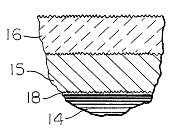
As seen in Figs. 1-4, a preferred embodiment of the charge
donor roller 10 has a core 14, and a bonding layer 15 of 1 to 3
mils thickness (1 mil = .001 inches) over the full outer surface
of the core 14. The core material in the preferred embodiment
is aluminum, but stainless steel, brass, some steels, glass, or
an FRP composite type material can also be used.
A ceramic layer 16 of 6 to 10 mils thickness is applied
over the full outer surface of the bonding layer 15. A seal
coat 17 is applied to penetrate the surface of the ceramic layer
as seen in Fig. 4.
The charge roller 10 is made as follows:
~teQ 1. Grit blast surface 18 of core 14 to clean and
roughen it to about a 200 to 300 microinch Ra surface.
Step 2. Apply a bonding layer 15 from 1 mil to 5 mils
thickness of a nickel-aluminide material by plasma or thermal
spraying with a 300 to 400 microinch Ra surface finish such as .
Metco 450 or 480. This step is optional but will improve the
bond strength of the ceramic 16 to the core 14.
Step 3. Apply a ceramic layer 16 of 10 mils to 15 mils
thickness using a blend of alumina and titania and plasma
spraying techniques and equipment.
-6-
, CA 02146339 2000-03-17
WO 94/11791 214 6 3 3 9 PCT/US93/05311
This step is further carried out by spraying thin uniform
sublayers to arrive at a desired thickness of the ceramic layer
16. The thinnest practical layer of plasma sprayed ceramic for
an electrical grade coating having high integrity and uniformity
is about 5 mils. In thinner layers, the peaks of the bond coat
layer 15 may protrude through the ceramic layer 16. Plasma
sprayed ceramic can also be applied in much thicker layers, as
great as 100 mils.
The ceramic layer 16 has a substantially uniform,
predictable dielectric strength. For example, a 10-mil thick
blended ceramic coating made with the above-described method
would have a dielectric strength of at least 3000 volts (at
least 300 volts per mil), well in excess of what is needed for
use as a charge donor roller. The ceramic layer 16 can be made
as thick as necessary to provide the required dielectric
strength or other physical or mechanical requirements.
Resistance increases in direct proportion to the thickness
of the ceramic layer 16, but the capacitance of the ceramic
layer 16 decreases in direct proportion.
Thus, the time constant, the product of resistance (R) and
capacitance (C), does not change, or changes little, with ceramic
layer thickness for a uniform material.
By changing the ratio of the insulating ceramic to the
semiconductive ceramic in the blended ceramic layer 16, the time
constant of the ceramic layer 16 can be adjusted over a range
covering three orders of magnitude at low voltages and at least
one order of magnitude at high voltage (over 1000V). The ratio
can also be finely controlled relative to a selected value for
the time constant.
Because the resistance of the ceramic decreases somewhat as
the applied voltage increases, the applied voltage and current
parameters should be defined prior to blending of the ceramic to
achieve a target time constant.
The ceramic mixture consists of at least one insulating
ceramic and one semiconductive ceramic. Blends of more than two
materials are possible.
WO 94/11791 ~ . PCT/US93/05311
..
Alumina and zirconia are examples of oxide ceramics that
are insulating materials. These typically have volume
resistivities of 1011 ohm-centimeters or greater. As used -'
herein, the term "insulating" material shall mean a material
with a volume resistivity of 101 ohm-centimeters or greater.
As used herein, the term "semiconductive" material shall mean a
material with a volume resistivity between 103 ohm-centimeters
and 101 ohm-centimeters. Titanium dioxide (Ti02~ and chromium
oxide are examples of semiconductive or lower resistance
ceramics. These ceramics have volume resistivities typically of
108 ohm-centimeters or lower. There are many other examples of
materials in both categories that are commercially available.
These relatively high and low resistance materials can be
blended to achieve the proper balance of electrical properties
for the charge transfer roller application.
It is noted that plasma spray ceramic powders are not pure
materials. Even the purest alumina commercially available is
only 99.0 to 99.5 pure. Many grades of alumina contain
several percent by weight of other metal oxides. For example,
white or gray alumina may contain titania (titanium dioxide)
(Ti02)in amounts from less than 5~ up to at least 40~. An
increase in the percentage of titania in the blend lowers the
resistance of the material and increases its capacitance (but to
a lesser degree) thereby decreasing the time constant of the
material. Even though these materials are available as single
powders, they are still blends of various ceramics. The
electrical properties of the final ceramic layer are the sum of
the individual contributions to resistance, capacitance,
dielectric strength, etc. A single powder may be available that
would exactly meet the electrical requirements for the charge
transfer roller application. It would no doubt not be a pure
material.
The preferred ceramics are Metco 130 (87/13
alumina/titania) and Metco 131 (60/40 alumina/titania) in a
40/60 to 80/20 blend. Metco products are available from Metco
Corp., Westbury, NY. The electrical properties of the coating
_g-
WO 94/11791 ~ ~ ~ ~ ' PCT/US93/05311
are determined in large part by the ratio of alumina to titania
in the finished coating. These two materials are easy to blend
since they can be purchased in the same particle size range and
they have nearly the same density.
The equivalent powders from the Norton Company, Worcester,
MA, are 106 and 108. These are chemically the same as Metco 130
and 131 but do not yield the same electrical properties. The
same blend of Norton powders gives a lower resistance, a higher
capacitance coating and a lower time constant.
The probable reason is that the alumina and titania are not
prefused in the Metco powders where they are in the Norton
powders. The Metco powders fuse in the plasma flame giving a
somewhat different coating composition and different level of
homogeneity.
For any ceramic layer containing titania (titanium
dioxide), the resistance of the layer is also affected by the
spraying conditions. Titania can be partially reduced to a
suboxide by the presence of hydrogen or other reducing agents in
the plasma flame. It is the suboxide (probably Ti0 rather than
Ti02) that is the semiconductor in the ceramic layer 16.
Titanium dioxide is normally a dielectric material. The typical
average chemical composition of titanium dioxide is 1.8 oxygen
per molecule rather than 2.0 in a plasma sprayed coating. This
level (and thus the coating properties) can be adjusted to some
extent by raising or lowering the percent of hydrogen in the
plasma flame. The normal primary gas is nitrogen or argon while
the secondary gas is hydrogen or helium. The secondary gas
raises the ionization potential of the mixture, thus increasing
the power level at a given electrode current. For a typical
Metco plasma gun, the hydrogen level is adjusted to maintain the
electrode voltage in the gun between 74 and 80 volts.
Another successful blend of ceramics can be made from a
mixture of 95~ pure alumina, such as Metco 101 or Norton 110,
and chromium oxide, such as Metco 106 or 136. The ratio of the
two powders would normally be in the 50/50 to 80/20 blend range.
More care has to be taken with these powders since the chromium
_g_
WO 94/11791 ' PCT/US93/05311
oxide has a higher density and tends to separate in the powder
feeder.
Regardless of the mixture of powders used, the plasma spray
parameters should be suitably adjusted to insure that the blend
of materials in the finished ceramic layer 16 is the same as
intended. All of the powders mentioned do not require the same
power levels, spray distance, and other parameters. Thus,
adjustment of spray distance, for example, may increase the
deposit efficiency of one powder over the other and change the
material blend in the finished coating.
The values of the time constant and resistance of the
ceramic layer 16 are not linear with respect to the blend
percentage of the ceramics. In the case of Metco 130 and 131
powders, the resistance increases linearly along one slope to
about a 50/50 blend, then sharply increases along another slope.
Plasma sprayed ceramic coatings can be applied in one pass
(layer) of the plasma gun or in multiple passes. The normal
method for most types of coating applications is to apply
multiple thin coatings of ceramic and build up to the required
thickness. Although the ceramic layer described above has a
uniform ceramic composition, the sublayers of ceramic in the
resulting layer 16 do not have to have the same composition.
The coating can be designed to have a different resistance at
the surface than the average bulk of the material. This might
be done 1) to change the way a charge is held at the surface of
the roller without changing its bulk properties or 2) to
compensate for the increased resistance of a topical coating.
Step 4. While the roller is still hot from the plasma or
thermal spraying of the ceramic layer 16, a seal coat 17 is
applied to the ceramic layer 16 using a dielectric organic
material such as Carnauba wax or Loctite 290 weld sealant. The
sealant is cured, if necessary, (Loctite 290), with heat, ultra
violet light, or spray-on accelerators. The ceramic porosity
level is generally less than 5~ by weight (usually on the order
of 2~). Once sealed, the porosity level has a minimal effect on
the coating properties for this application.
-10-
WO 94/11791 ~ ~ ~ ~ ~ ~ ~ PCT/US93/05311
The preferred types of materials are 100 percent solids and
low viscosity. These include various kinds of waxes, low
'- viscosity condensation cure silicone elastomers, and low
viscosity epoxy, methacrylates, and other thermoset resins.
' 5 Liquid sealers such as silicone oil could be used alone, or
liquids in solids, such as silicone oil in silicone elastomer.
These may yield additional benefits to the charge transfer
roller to provide some measure of release (non-stick properties)
to toner, for example.
The sealer will generally be a high resistance material,
although the electrical properties of the sealer do affect the
overall properties of the sealed ceramic layers 16, 17. For
example, sealing with Carnauba wax will result in a higher
resistance of the sealed ceramic layer 16, 17 than Loctite 290
weld sealant because it is a better dielectric material. It is
also possible to use a semiconductive sealant with a dielectric
ceramic (without any semiconductive ceramic) to achieve the
desired electrical properties.
A low resistance sealer could be used, such as a liquid or
waxy solid type of antistatic agent, as long as the combination
of ceramics and sealer yielded the proper electrical properties
in the completed ceramic layer 16.
Topical coatings can also be applied to the roller 10 to
provide additional properties and functions as long as the
designed electrical properties can be maintained. For example,
a thin layer of a Teflon~ polytetrafluoroethylene (PTFE)
material (possibly 1 mil thick or less) could be applied to the
finished roller to provide release to the roller 10 surface or
change the coefficient of friction. The effect on the roller
would be minimized if the PTFE were very thin or if peaks of the
ceramic protruded through it.
5) A final step is to grind and polish the sealed ceramic
layer 16, 17 to the proper dimensions and surface finish
(diamond, silicon carbide abrasives, etc.). After finishing,
the ceramic layer 16, 17 is typically 6 to 10 mils thick with a
surface finish 20 to 70 microinches Ra. In other embodiments,
-11-
CA 02146339 2000-03-17
WO 94/11791 2 ~ ~ 6 3 3.9 PGT/US93/05311
it may be thicker than 10 mils and vary in surface roughness
from 10 to 250 microinches Rte.
The physical and electrical properties of the ceramic do
not deteriorate over time or due to exposure to oxygen,
moisture, or chemicals resulting in a long useful life for the
product. Improved temperature resistance is also expected over
anodized surfaces. Ceramic surfaces can perform at 600° F
consistently with slight effects on the electrical properties.
This has been a description of examples of how the
invention can be carried out. Those of ordinary skill in the
art will recognize that various details may be modified in
arriving at other detailed embodiments, and these embodiments
will come within the scope of the invention.
For example, although the invention is described with
IS reference to a xerographic copy machine, the invention may have
utility in other types of machines using image transfer rollers.
Therefore, to apprise the public of the scope of the
invention and the embodiments covered by the invention, the
following claims are made.
The term Ra used above is a recognized abbreviation for
average roughness under ASME standards.
-12-
__. __._ .~ _ _~ __. _ ._.. _ ._ ~_