Note: Descriptions are shown in the official language in which they were submitted.
2146921
1 LOW-LOSS CLAMP CIRCUIT
2 BACKGROUND OF THE lNV~NlION
3 Clamp circuits have been used in a number of prior art
4 circuits. They may also be considered snubber circuits
which limit a voltage across a circuit element. In DC to
6 DC converter circuits, semi-conductor switches are used to
7 control the flow of energy. When the switch is opened an
8 inductance is in the circuit, such as a transformer
9 primary, a high voltage is generated across the switch as
it turns off. The prior art clamp circuits have in some
11 cases used a capacitor in circuit across the semi-conductor
12 switch, perhaps with a diode in circuit therewith but also
13 a resistor feeding power back to the input voltage source.
14 This resistor dissipates energy rather than positively
utilizing that energy.
16 The U.S. Patent No. 3,297,960 to Massey, shows a
17 converter which uses a pair of diodes 1 and 2 to prevent
18 saturation of a transistor 3 by maintaining a near zero
19 voltage across the base and collector. The diodes are
connected directly to the secondary of the power
21 transformer to provide current and voltage feedback.
22 Massey does not show the energy storage configuration of
23 the present invention.
24 SUMMARY OF THE INVENTION
The invention relates to a low-loss clamp circuit for
26 a converter. Specifically, this may be a DC to DC
27 converter which is current fed. A push pull converter is
28 shown with two semi-conductor switches, and when one of
29 these two switches opens, the voltage thereacross is
clamped to the voltage of a clamp capacitor, and the energy
31 across this capacitor is returned to the secondary circuit
32 of a transformer so that the circuit has very low loss.
2146921
1 Accordingly, an object of the invention is to provide
2 a clamp circuit for a converter wherein energy of the clamp
3 circuit is not lost in a resistance connected to the
4 primary winding to a transformer. Instead it is fed into
the secondary circuit which supplies a load voltage.
6 More specifically, the invention is directed to a low
7 loss clamp circuit for a DC to DC converter. The converter
8 including a transformer with a secondary winding in a
g secondary circuit and center tapped primary winding, the
primary winding center tap and a circuit ground being
11 energizable by a DC voltage input, a rectifier connected to
12 the secondary winding and to the circuit ground to supply a
13 DC output voltage, a pair of semiconductor switches each
14 having input and output electrodes, each end of the primary
winding being connected through a respective switch to
16 circuit ground; each switch having a control electrode
17 connected to a control circuit, said clamp circuit
18 comprising: a pair of diodes connected cathode-to-cathode
19 across the input electrodes of the switches at a clamp
junction; a clamp capacitor connected between said clamp
21 junction and said circuit ground and; energy return means
22 connected to said clamp junction to return energy from said
23 clamp capacitor to said secondary circuit.
24 Other objects and a fuller understanding of the
invention may be had by referring to the following
26 description and claims, taken in conjunction with the
27 accompanying drawings.
28 BRIEF DESCRIPTION OF THE DRAWINGS
29 FIG. 1 is a schematic drawing of a prior art clamp
circuit which dissipates energy;
31 FIG. 2 is a schematic diagram of a clamp circuit which
32 is a low loss circuit according to the invention;
33 FIG. 3 is a modification of the invention;
34 FIG. 4 is a wave form diagram of voltages across the
switches;
2146921
1 FIG. 5 is a wave form diagram of primary winding
2 currents through the switches;
3 FIG. 6 is a wave form diagram of the voltages on the
4 secondary winding;
FIG. 7 is a wave form diagram of the secondary winding
6 currents;
7 FIG. 8 is a wave form diagram of the secondary center
8 tap current;
9 FIG. 9 is a wave form diagram of the current through
the clamp diodes;
11 FIG. 10 is the control circuit gate drive wave forms
12 on the switches;
13 FIG. 11 is wave form diagrams of the primary center
14 tap voltage and the input choke current;
FIG. 12 is a schematic diagram of a second
16 modification;
17 FIG. 13 is a schematic diagram of a third modification
18 of the invention;
19 FIG. 14 is a graph of duty cycle D of the FET
switches;
21 FIG. 15 is a graph of calculated efficiency as a
22 function of input voltage;
23 FIG. 16 is a graph of total power dissipation of the
24 FET switches; and
FIG. 17 is a graph of clamp capacitor voltage as a
26 function of input voltage.
27 DESCRIPTION OF THE PREFERRED EMBODIMENTS
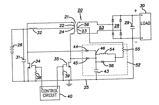
28 FIG. 1 illustrates a prior art clamp circuit which
29 dissipates energy. FIG. 1 illustrates a converter circuit
which converts energy from one form into another form. In
31 this case, the converter is a current fed DC to DC
32 converter 20 which converts a low input DC voltage to a
33 higher output DC voltage. This is accomplished by a
34 transformer 21 which has a center tapped primary winding 22
and a secondary winding 23. The primary winding center tap
--3--
6g21
1 24 and a common circuit ground 25 are energized from a DC
2 voltage source 26. The two ends of the secondary winding
3 are connected to a rectifier 28, in this case a bridge
4 rectifier with a filter capacitor 29 connected across the
rectifier for smoothing of the output voltage which then is
6 connected to a load 30. A smoothing capacitor 31 is
7 connected across the input voltage, and a series choke 32
8 is connected between the positive end of the voltage input
9 and the center tap 24. Semi-conductor switches 34 and 35
are connected in push-pull to the ends of the primary
11 winding 22. These semi-conductor switches may be bipolar
12 transistors, gate turn-off thyristors, or as shown, may be
13 field effect transistors. The two power electrodes of the
14 switches are connected between the ends of the transformer
primary winding and the common ground 25. With the FET's
16 as shown, the drains are connected to the primary winding
17 and the sources are connected to the ground 25. Gate drive
18 resistors 38 and 39 are connected between the respective
19 gates and ground.
A clamp circuit 42 clamps the voltage of the switches
21 34 and 35 to the DC voltage of a clamp capacitor 43. Clamp
22 diodes 44 and 45 conduct current when the voltage across
23 the respective switch exceeds the clamp voltage on the
24 clamp capacitor 43. A clamp junction 46 is at the
connection 43 to the cathodes of the clamp diodes. From
26 this clamp junction, a clamp resistor 47 is connected to
27 the primary circuit, in this case, the positive terminal of
28 the input voltage. The disadvantage of this prior art
29 circuit is that the clamp resistor 47 dissipates energy
which lowers the efficiency of the converter.
31 FIG. 2 is a schematic diagram of a clamp circuit for a
32 converter according to the invention. For convenience, the
33 converter itself is the same as described for the prior art
34 of FIG. 1, the clamp circuit 52 is, however, different.
Also in this converter 20, a control circuit 40 has been
36 added to supply the gate voltages. In the clamp circuit,
37 the clamp diodes 44 and 45 are again connected together at
--4--
-- 2146921
1 the cathodes at a clamp junction 46. The clamp capacitor
2 43 is again connected between the clamp junction 46 and the
3 common ground 25. The energy stored in the clamp capacitor
4 43, however, is connected to return energy to the secondary
circuit 53 through an inductance 54 and a resistor 55 to a
6 center tap 56 on the secondary winding 23. A protective
7 diode 56 is connected across the inductance 54 with the
8 cathode connected to the cathode junction 46. In this
9 case, the energy is returned to the secondary circuit for a
low loss clamp circuit which eliminates the loss in the
11 prior art circuit and, thus, makes a more efficient
12 converter.
13 FIG. 3 shows schematically another clamp circuit 62.
14 This has the clamp diodes 44 and 45 and the clamp junction
46 with the clamp resistor 55 connected between the clamp
16 junction 46 and the positive output voltage terminal 63.
17 In this case, the energy from the clamp capacitor 43 is
18 returned to the secondary circuit at the output voltage
19 terminal. Assuming that the transformer is a step-up
transformer, this clamps the voltage across the switches 34
21 and 35 to the output voltage rather than to the center tap
22 of the secondary. This has the advantage of not requiring
23 a center tapped secondary but has a disadvantage of
24 clamping the voltage across the switches at a higher
voltage.
26 The basic operation of the main circuit of Fig. 2
27 requires that both switches 34 and 35 be on together for a
28 certain amount of time. Then only one of the two switches
29 is turned off. During this off time current flowing in the
input inductor 32 flows through 1/2 the primary of the
31 transformer and induces current to flow in the secondary.
32 The secondary current then passes through the rectifier
33 bridge 28 and to the output load.
34 When switches 34 or 35 turn off, the voltage across
these devices will increase rapidly until they reach the
36 steady state voltage of the clamp capacitor 43, e.g. 200 V.
37 When this happens clamp diodes 44 and/or 45 will conduct
2146921
1 and thereby set the maximum voltage of the switches to the
2 clamp capacitor voltage. The voltage across the switches
3 will remain clamped until the current in the transformer
4 winding connected to the off switch decays to zero. The
time it takes for the current to decay to zero is
6 relatively short compared to the time duration of one
7 cycle. As the transformer current is decaying to zero, it
8 flows through one of the clamp diodes 44 or 45. The
9 current then flows into the clamp capacitor 43 which
increases the charge and energy level of this capacitor.
11 This increased charge and associated energy is removed from
12 the clamp capacitor when only one of the two switches 34 or
13 35 is on and the other one is off. During this time the
. ..
14 transformer secondary winding 23 is conducting current to
the output load through the bridge rectifier diodes. The
16 secondary winding voltage is therefore the output voltage
17 value. The primary winding voltages and also the voltage
18 across the off switch are determined by the turns ratio of
19 the transformer and the secondary winding voltage. The
secondary center tap voltage during this time will be about
21 1/2 the output voltage. This voltage value will be
22 slightly lower than the clamp capacitor voltage. This
23 condition forces current to be drawn out of the clamp
24 capacitor 43 through inductor 54 and resistor 55 in Fig 2.
This current flows into the secondary winding center tap.
26 Through auto-transformer action this center tap current
27 flows through the bridge rectifier diodes to the load and
28 back to the clamp capacitor 43 which discharges the
29 capacitor. The inductor 54 causes the current to be drawn
out of the clamp capacitor smoothly instead of in the form
31 of large spikes. The diode 56 across the clamp choke 54
32 provides a path for the choke current to flow when the
33 clamp capacitor is not discharging. The resistor 55 is an
34 impedance to limit surge current when the DC input voltage
is first applied.
36 At the end of each conduction overlap period when one
37 of the FET switches turns off, and voltages are developed
21~6921
1 across the transformer, spike voltages will appear across
2 the FETs that are greater than the predicted peak values.
3 These spikes are generated by the energy stored in the
4 transformer leakage and wiring inductances. Diodes 44 and
45 and capacitor 43 provide a path for current flow when
6 the FETs are turned off. The current that flows through
7 these components only lasts for the time that it takes for
8 the secondary current to build up to its normal value (i.e.
9 input inductor current times Np/Ns). The leakage
inductance determines this time. The clamp capacitor 43
11 prevents the voltage across the FETs from going too high
12 during the time that current is flowing into it.
13 A discharge path for the clamp capacitor must be
14 established for the voltage across the clamp capacitor (and
FET's), or this voltage will rise to an unacceptable value.
16 One method of accomplishing this is to simply connect the
17 top of the clamp capacitor to the output voltage, as in
18 Fig. 3. This is an energy return means to the secondary
19 circuit. This approach limits the maximum clamp voltage to
the output voltage. This voltage magnitude may be too high
21 for many applications. If the clamp capacitor is connected
22 to the secondary center tap, as in Fig. 2, then current
23 will be discharged to the output whenever the secondary
24 winding is clamped to the output. Current will flow
through the secondary winding by auto transformer action as
26 long as the secondary current is higher than 1/2 the clamp
27 current. Inductor 54 (reference figure 2) controls the
28 flow of current to the secondary center tap when the
29 secondary winding is clamped to the output and the clamp
capacitor is discharging. The bypass or protective diode
31 56, across the clamp inductor 54, provides a path for the
32 inductor current to flow when the secondary winding is not
33 clamped to the output and the clamp capacitor is not
34 discharging. The resistor 55 in series with the center tap
serves to limit the start up surge or inrush current
36 through the clamp circuit when input voltage is first
37 applied to the power supply during initial turn on.
21~6921
1 The following waveforms illustrate the operation of
2 the power circuit during the steady state operation that
3 was previously discussed.
4 Fig. 4 illustrates the wave forms of the voltages
across switches 34 and 35. One will note that the voltages
6 are clamped at about 200 volts. The voltage humps 65 occur
7 when the switch 34 is off so that there is a voltage across
8 this switch. The humps 66 occur when the switch 35 is off.
9 The practically zero voltage areas 67 occur when both
switches 34 and 35 are on.
11 Fig. 5 shows wave forms 68 of the primary winding
12 current through switch 34 and wave form 69 shows the
13 primary winding current through switch 35. Note that the
14 currents drop to about one half the peak value when both
switches are on.
16 Fig. 6 shows wave forms 71 and 72 of the secondary
17 voltages taken from each end of the secondary winding to
18 common. Note how the secondary winding voltages are
19 clamped to output voltage of about 400 volts.
Fig. 7 shows a wave forms 73 and 74 of the secondary
21 winding currents. These wave forms depict the currents
22 measured at each end of the secondary winding.
23 Fig. 8 shows the wave form 75 of the current flowing
24 into the secondary center tap. It is also the current that
is discharging the clamp capacitor 43.
26 Fig. 9 illustrates wave forms 76 and 77 of the current
27 flowing through the diodes 44 and 45 respectively. It is
28 also the current flowing into and charging the clamp
29 capacitor 43.
Fig. 10 shows the wave forms 85 and 86 of the gate
31 drive of the switches 34 and 35 respectively. These gate
32 drives show the overlap condition in the area 78.
33 Fig. 11 shows a wave form 79 of the input choke
34 current which is primarily DC with a small amount of AC
ripple. The primary center tap voltage is shown in wave
36 form 80 that it goes higher than the input voltage, which
--8--
- - -
2146~21
1 is the reference line 81 through the middle of the voltage
2 trace.
3 Fig. 12 is a schematic diagram of another clamp
4 circuit 82 wherein the connection of the clamp circuit to
the secondary winding is not at a mid-tap, but at two
6 equally spaced points 83 and 84 from the mid-tap. This
7 achieves a lower clamping voltage if desired. The
8 operation of the clamp circuit is basically the same but
9 now the clamp capacitor 43 will be discharged to a lower
voltage as determined by the turns ratio of the secondary
11 taps 83 and 84.
12 Fig. 13 is a third modification which utilizes an
13 auxiliary winding 90 with an additional bridge rectifier gl
14 connected to the positive output terminal. The clamp
circuit 92 is connected to the negative of this auxiliary
16 winding. The auxiliary winding turns ratio can be adjusted
17 to allow clamping voltages that are higher or lower than
18 the original circuit of Fig. 2.
19 ANALYSIS:
The following equations describe the important
21 parameters for design analysis purposes: They were derived
22 under steady state conditions for continuous boost mode
23 operation using math cad.
24 Variable definitions:
Vo:=395 output voltage
26 Vd:=1.5 diode drop voltage for all
27 diodes
28 M:=5 step up transformer turns
29 ratio, total secondary to
1/2 primary.
31 L:=10 10-fi inductance of input inductor
32 V~:=38,40.. 72 input voltage range values
33 P~:=1500 assumed input power
34 Rc:=.Ol input choke winding
resistance
- ~146921
1 R,:=.03 resistance of 1/2 of the
2 transformer primary
3 C~:=5 10-6 input filter capacitance
4 F5:=250 103 switching frequency at
rectifier output (ie. 2xFET
6 freq.)
7 LC =5 1O-6 leakage inductance as
8 measured from total secondary
9 to total primary windings
Rc~p:=l resistance of clamp resistor
11 C:=2 10-6 capacitance of clamp
12 capacitor
13 Rd:=.03 on resistance of Fets M1 and
14 M2. There are 8 FETs used, 4
in parallel for each M1 and
16 M2. Each FET is rated at 300
17 volts, 40 amps and .12 ohms
18 RDS(O~ @ 100 deg C. IXTH4N30
19 from IXYScorp.
C~55:=1350 10-l2 FET junction output
21 capacitance for 4 parallel
22 devices
23 E(I~)= Efficiency
24 Basic equations~ continuous mode boost operation
M M V M2 Vin t c d in
[ M +2 Md+2 V (Rt+Rd)]
26 Duty cycle as a function of input voltage vin. Duty cycle
27 defined as overlap time divided by switching
28 frequency period.
--10--
21~6921
1 eq 2) Vtap = VO 2 Vd
2 peak value of voltage from primary center tap 24 to common
3 25 excluding voltage spikes and ringing
4 eq 3) Vf~,:=2 V~p
peak value of FET drain to source voltage of switch 33 or
6 34 excluding spikes and ringing
7 eq 4) Iin(Vin) = V dc input current
8 eq 5) ILPP( Vin) = [ Vin~ Iin( Vin) ~(Rc+ 2 + 2d ~ ] ' L Fn
9 peak to peak value of ac ripple current in input choke 32
eq 6) in in 8 Cin' FS
11 peak to peak value of ac ripple voltage across input filter
12 capacitor 31 assuming all choke 32 ac ripple current is
13 bypassed through the input filter capacitor 31
14 eq 7) ( ) ILPP ( Vin) ~
rms value of ripple current through input capacitor 31
16 assuming all choke ripple current flows in the input filter
17 capacitor.
-- 21~6921
eq 8) IF~Ms( Vin) : = in 2 in ~/2 - D ( Vin)
2 rms value of current flowing through fets 34 or 35
3 eq 9) Pon( Vin): =2 Rd IFR~S ( Vin)
4 Total FET conduction ~ON STATEII losses of both 34 and 35
eq 10) p = Vfet-FsCoss
6 FET switching losses during the turn on and discharge of
7 CO~. (Turn off losses assumed to be zero)
8 eq 11) p~( Vin) : =PS+Pon ( Vin) total FET 34 and 35 losses
9 eq 12) Pe( Vin) : = 2 Le-( in( in) ) .F
power associated with leakage inductance trapped energy
11 eq 13) PO ( Vin) : = in M in (1 -D ( Vin))Vo+Pe ( Vin) output power
12 eq 14) E(V ) Po(Vin) overall efficiency
13 eq 15) I (Vi) = P(Vin) average output current
-12-
21~6921
eq 16) IpK( Vin) l-D(V ) secondary 23 peak current
2 eq 17) ISRMS ( Vin ) =IPK( Vin)-~/1 -D ( Vin)
3 secondary 23 rms current
4 eq 18 ) ICOR~S ( Vin) =~IISR~S( Vin) 2-Io ( Vin)2
output capacitor 29 rms current
6 eq 19) PRD( Vin) IPK( Vin) 2Vd-(1--D( Vin))
7 total output rectifier 28 diode losses
V ( V ) V D ( Vin) VO
9 clamp capacitor 43 voltage if Rclp 55 were equal to zero
eq 21) VClp( Vin) = 1( in) Vfet +
11 ( Vl( Vin) ~ Vfet). 1 + ( RclpPe( Vin) ).( 2 )2
2 ~ 1 -D ( Vin) Vl( Vin) ~ Vfet
12 total clamp capacitor 43 voltage
13 eq 22) T (V ) = 2LeIn(Vin) 10
14 leakage inductance delay time in microseconds
-13-
21~6921
eq 23) IC1P( Vin) : = in 4 in Td( Vfn) Fs-10-6
2 average clamp current
3 eq 24) ICpk( Vin) l _D ( Vi )peak clamp current
4 eq 25) IClprms( Vin) = Icpkt Vin) ~/1 -D ( Vin) rms clamp current
eq 26) ICaprms( Vin) : =~ ( in 2 in )2~ Td ( Vi ) ' 10 _6 ~ Fs -I ( V ) 2
6 rms current in clamp capacitor 43
7 eq 27 ) Prclp ( Vin ) = IclprmS ( Vin) 2'Rclp
8 clamp resistor 55 power dissipation
9 eq 2 8) Pdclp(Vin) = Icpk(V"~) Vd D(V~
10 dissipation of diode 56 across clamp choke 54
11 eq 29) P ( V ) = Iin( Vin) , T ( V ) ~ F ~ V ~ 10 -6
12 dissipation of clamp diodes 44 and 45
13 eq 30) ~ Vclp( Vin) = in( Vin) , Td( Vfn) ~10
14 ripple voltage on clamp capacitor 43
- 14 -
2146921
o
oo
g
-
o
._
~ t o ~ ~ ~ o ~ ~ -- ~ o~ o t--
P~
In
: 11'~3 'I
r~ ~ ~ oo
C ~ ~ ~ -- O O ~ 00 00 t-- l-- ~ \D U~ ~ ~ ~i
~_ ~ C`~ ~ C`l C`l -- _ _ _ _ _ _ _ _ _ _ _ _
~, ~ c~, c~ ~ - - o o~ c - ~ ~ ~ ~ o
~9
o 9 c~ '~ ~ ~ ~ c~ o oo ~o ~ ~o ~ l - ~ ~ ~ ~
~ ~o ~ o o o o o o o o o o o o o o o o o o
~3 o ~9
~ ~ v _ ~ c~ ~ O ~ v~ l O ~ ~ oO a~ ~ ~ oo
.S ~, ~ ~ O oo V ~ O ~O C~ 1~ ~ r` -- vl
C~
~C ~o ~ o ~ C~ oo ~ O ~ X
o o o o c; o o o o o o o o o o o o o
`l
21~6921
-
~ ~ ~ ~OD ~ ~ -- ~ g
ooooooooooooooooo_
_~_I4___~___~_____
-3
:,
c~ ~ o oo oo O ~ oO ~ a~ v~ ~ O t~ ~
o 00 U~ ~ O 00 ~ ~ ~ ~ ~ ~ C`l _ _ _ _1 0 0
~___oooooooooooooo
~ - - - o o o o o o o o o o o o o o o
-3
~> ~ - - - - - o o o o o o o o o o o o
-3
e o ~ o o~ ~ O c~l ~ O ~ O ~ ~ o~ ~ ~ ~1 a~
------OoOoOOOoOOOooOo
OoOOOOOOOOOOOOOC;OO
-- ~ O G O ~ 0~ oo oo oo oo oo oo oo
o o o c o o~
~____~___~_~___
oo ~ _ ~ ~ ~ ~ O O~ n ~ ~ ~ ~ ~ O
~ oo o ~ ~ ~ oo o ~ ~ ~ oo o ~ ~ ~ oo o ~
~ ~ - ~ ~ ~o r a~ ~ o ,I N ~ ~ In ~ I` a~ ~n
2146921
~ ~ ~ oo ~ V~ o U~ o V~ ~ ~ ~ oo ~ ~ o~
8 ~ ~ ~ ~ ~ o oo t-- ~ ~ ~ ~ a~ oo 1-- ~ ~
oooooooooooooooooo
~ 1` ~ ~ ~ ~ ~ ~ c~ ~ O O a~ a~
~3
t-- ~ ~ o o -- ~ ~ o ~t ~ ~ o `o c`~
~ - - ~ - ~ - ~ o o o o o o o o o o
t
oo ~ c~ o oo t-- ~ ~ ~ ~ c~ ~ -- ~ -- ~ o o
~ - ~ - ~ o o o o o o o o o o o o o o
E~ oooooooooooooooooo
.5 oO O ~ 'J `D 00 0 ~ ~ ~D oO O ~ ~ ~ 00 0 C`l
2146921
1 Some of the more important values from the charts of
2 pages 15 - 17 may be graphed in Figs. 14 - 17. Fig. 14
3 shows a curve 9S of the calculated duty cycle of the
4 primary FET switches, and shows that it varies linearly.
Fig. 15 shows a curve 96 of the calculated efficiency and
6 shows that it increases as the input voltage increases.
7 Fig. 16 shows a curve 97 of the total power dissipation of
8 the FET switches. Fig. 17 shows a curve 98 of the clamp
g capacitor voltage as a function of input voltage.
What has been described above in the formulas and
11 tables refers to a boost mode of operation. This is when
12 for a certain portion of the duty cycle both FET switches
13 34 and 35 are conducting simultaneously.
14 A second mode of operation may be referred to as a
buck mode. If both of the FET's are turned off for a
16 portion of each half cycle, and then alternately, one FET
17 at a time is turned on for the remainder of each half
18 cycle, the output voltage may be sustained at values below
19 the minimum boost mode voltage. This buck mode of
operation is required to limit the in-rush current when the
21 input voltage is first applied. The clamp circuit still
22 functions and energy is transferred to the output from the
23 clamp capacitor when one FET 34 or 35 is turned on. A
24 third mode of operation exists for very low output voltages
wherein the clamp capacitor voltage becomes equal to the
26 output voltage instead of one half the output voltage.
27 This is caused by the clamp circuit current that flows into
28 the secondary center tap. During this third mode of
29 operation the magnitude of the clamp current is greater
than two times the input inductor current reflected through
31 the secondary winding and this results in the transformer
32 clamping to zero volts across all windings. This produces
33 a form of boost operation even though the FET switches are
34 being modulated in the buck mode. However, the output and
clamp capacitor voltages can never be lower than the input
36 voltage.
-18-
2146921
1 The following is a list of components of a circuit
2 embodying the invention shown in Figure 2 as a workable
3 circuit.
4 LIST OF COMPONENTS
5 L32 10 ~H
6 LCIP54 50 ~H
7 R3s~3s 1 K OHM
8 RCIP 55 1 OHM
9 All DIODES DMOD
C~ 31 5 ~fd
11 Cclp 43 2 ~fd
12 CO 29 1000 ~fd
13 It will be noted that the primary circuit and the
14 secondary circuit are tied together at two points; one
being the common ground at 25 and the other being the clamp
16 voltage being applied in various ways to the secondary
17 circuit. This is necessary in order that the energy stored
18 in the clamp capacitor 43 is fed back to the output. This
19 is a main advantage of the present circuit in that there is
a very low loss, perhaps only 10% of a standard clamp
21 circuit of Figure 1 because in Figure 1 the clamp capacitor
22 43 is tied back to the primary circuit, which produces high
23 power dissipation in the clamp resistor 47. As a result
24 one limitation of the circuit is that the primary and the
secondary circuits can not be isolated, even though a
26 transformer is used. Please note that there are eight FET
27 switches, four in parallel as the switch 34 and four more
28 in parallel as the FET switch 35. This is in order to
29 achieve the 1400 watt output capacity.
The present disclosure includes that contained in the
31 appended claims, as well as that of the foregoing
32 description. Although this invention has been described in
--19--
- 21~6921
1 its preferred form with a certain degree of particularity,
2 it is understood that the present disclosure of the
3 preferred form has been made only by way of example and
4 that numerous changes in the details of construction and
the combination and arrangement of parts may be resorted to
6 without departing from the spirit and the scope of the
7 invention as hereinafter claimed.
-20-