Note: Descriptions are shown in the official language in which they were submitted.
W O 94/10743 2 1 4 6 9 8 7 PC~r/US93/09343
_ 1 _
LOAD CURRENT FUNDAMENTAL FILTER WITH
ONE CYCLE RESPONSE
Brief Descri~tion of the Invention
This invention relates generally to a method and apparatus
for providing low distortion power signals. This invention
more particularly relates to a one cycle response filter for
deriving a feed-forward load current fundamental signal
which is subtracted from an instantaneous load current
signal to obtain a load current harmonic signal which is
used as a reference signal by a parallel inverter of an
active power line conditioner.
Back~round of the Invention
Power electronic circuits are used to control and condition
electric power. For instance, power electronic circuits may
be used to convert a direct current into an alternating
current, to change voltage or current
magnitude, or to change the frequency of an alternating
current.
An inverter is a power electronic circuit which receives a
dc source signal and converts it into an ac output signal.
Harmonic neutralization and pulse-width modulation
techniques are used to generate the ac signal. Harmonic
neutralization involves a combination of several phase-
shifted square-wave inverters, each switching at the
fundamental frequency. Pulse-width modulation involves
~ ~ ~6g~ -2- PCT/US93/09343
switching a single inverter at a frequency many times higher
than the fundamental.
Filters can be classified according to whether their main
purpose is to improve the power waveform or to remove EMI.
Filters for waveform improvement usually deal with
frequencies in the audio range. EMI filters are usually
concerned with frequencies of 455 kHz or higher.
Passive filters are typically used to eliminate undesirable
harmonics from the inverter output. Unfortunately, passive
filters do not provide continuous harmonic filtering on
pulsating or randomly varying loads. This occurs because
passive filters only adapt to new harmonic levels after a
considerable settling delay.
Passive filters tend to be large, heavy, costly, and, in
general, highly load-dependent. Consequently, passive
filters frequently represent a substantial part of the total
cost, weight, and size of power electronics equipment.
Active filters represent an emerging technology without many
of the shortcomings associated with passive filters. The
technology relies upon the theory of active-feedback
filters. A feedback loop with a single energy-storage
element (an inductor or capacitor) is used to minimize the
difference between the actual waveform and the desired
waveform.
The urgency of developing successful active power filters
has recently grown in view of the increasing waveform
distortion of both voltages and currents in ac power
distribution systems. These distortions are largely
attributable to a growing number of nonlinear loads in the
electric utility power network. Typical nonlinear loads are
computer controlled data processing equipment, numerical
controlled machines, variable speed motor drives, robotics,
medical and communication equipment.
WO94/10743 3? 1 4 6 9 8 7 PCT/US93/09343
Nonlinear lGads draw square wave or pulse-like currents
instead of purely sinusoidal currents drawn by conventional
linear loads. As a result, nonlinear current flows through
the predominantly inductive source impedance of the electric
supply network. Consequently, a non-linear load causes load
harmonics and reactive power to flow back into the power
source. This results in unacceptable voltage harmGnics and
load interaction in the electric power distribution in spite
of the existence of voltage regulators.
The degree of current or voltage distortion can be expressed
in terms of the relative magnitudes of harmonics in the
waveforms. Total Harmonic Distortion (THD) is one of the
accepted standards for measuring voltage or current quality
in the electric power industry.
Apart from voltage and current distortion, another related
problem may arise when nonlinear loads are connected to the
electric power network. In particular, when the load
current contains large amounts of third or other triplen
harmonics, the harmonic current tends to flow in the neutral
conductor of the power system. Under these conditions, the
neutral current can exceed the rated current of the neutral
conductor. Since the neutral is normally designed to carry
only a fraction of the line current, overheating or even
electric fires can result.
As previously indicated, active filters may be used to
alleviate these problems. Active filters, or active power
line conditioners (APLCs) comprise one or two pulse width
modulated inverters in a series, parallel, or series-
parallel configuration. The inverters share a common dc
30 link, which can be a dc inductor-(current link) or a dc
capacitor (voltage link). It is advantageous to keep the
energy stored in the dc link (capacitor voltage or inductor
current) at an essentially constant value. The voltage on
the dc link capacitor can be regulated by injecting a small
35 amount of real current into the dc link. The injected
W094/10743 ~69~ 1 -4- PCT/US93/09343
current covers the switching and conduction losses inside
the APLC. The link voltage control can be performed by the
parallel inverter.
The basic active load current compensation with current or
voltage source filters is known. Figure l depicts a
parallel connected current source active filter 20, and
Figure 2 depicts a parallel connected voltage source active
filter 22. The load current IL consists of three
components: The real current, Irl the reactive current, Iq/
and the ripple current, IR. The parallel connected active
filter supplies the IR and Iq components, and, also, a small
residual "high frequency" component Ihf, that flows into the
parallel connected "high frequency" capacitor Chf. The
parallel connected active filter is essentially a single
phase inverter which is operated from an isolated current or
voltage source.
The realization of the active filter requires solid state
switches with intrinsic turn-off capability (transistors,
IGBTs, MOSFETs, GTOs, etc.). Switch pairs Pl and P2 are
alternately turned ON or OFF. The average voltage required
in the link capacitor, VdCl of Figure 2, is supplied by the
ac source. Real power can be absorbed by introducing an
appropriate amount of offset in the symmetry of the on-times
in switches Pl and P2. The polarity of the offset is
coordinated with the polarity of the input voltage. When
switches Pl of Figure 2 are on, a current is generated
between the tie inductor, Lp, the output capacitance
dominated by Chf, and the difference between the dc link and
ac output voltages. Conversely, when the P2 switch pair is
on, the current is driven by the sum of the dc link and ac
output voltages.
The real power, necessary to maintain the selected dc link
voltage magnitude, Vdc, is proportional to the average duty
cycle of high-frequency pole switchings in any given half
line voltage cycle. The isolated dc link voltage is
WO94/10743 21 4 6 9 8 7 PCT/US93/09~3
--5--
regulated by a closed loop controller that affects the
average pole switching symmetry. Reactive inverter currents
can be produced that flow in or out of the inverter by
temporary changes in the duty cycle of inverter pole
s switchings. The instantaneous magnitudes of inverter
currents are reaulated so that they provide the load
compensation current requirements. For example, if a
positive ripple current is detected, the on-time of P2 is
increased with respect to Pl. The increase results in the
required net compensating ripple current flowing in the ac
line. This also implies that the amplitude of Vdc must be
kept higher than the highest value of the ac voltage across
the load, otherwise, the instantaneous compensation
capability of the acti~re filter is impaired.
The rapid pulse width modulation switching in the active
filter produces a high frequency, triangular shaped current,
Ihf, an undesired side effect. The effect of the Ihf signal
is a small, superimposed triangular voltage ripple on the ac
voltage. The amplitude of the voltage ripple is inversely
proportional to the pole switching (carrier) frequency and
the value of Chf. The voltage ripple is filtered with a
parallel capacitor Chf.
When the active power filter (20 or 22) is connected across
the load, a high degree of filtering of the terminal voltage
is observed. Note that the active power filter is not
capable of supplying or absorbing any real power other than
that which is needed to compensate for losses inside the
filter itself. It will, however, readily compensate
reactive currents, non-synchronous and non-theoretical
harmonics and sources with variable or unregulated
frequency. The shunt connected power circuit is inherently
protected under load short circuits since the load fault
current bypasses the active power filter.
The isolated dc link circuits of Figures l and 2 can be
combined to produce an ac line conditioner and voltage
W O 94/10743 ~69~ PC~r/US93/09343
regulator. Figure 3 depicts a shared link current source
active power filter 24 with a serial inverter 26 and a
parallel inverter 28. Figure 4 depicts a shared link
voltage source active power filter 30, with a serial
inverter 32, and a parallel inverter 34. The respective
~ series and parallel inverters are similar to the filters
described in relation to Figure 1 and 2. The shared link
approach of Figures 3 and 4 represents a combination of
series and shunt connected filters which are operated from
a common shared direct voltage (or current) source.
The shared link circuit topology removes the former
limitation of the active power filter, namely, that it is
not capable of supplying or absorbing any real power, apart
from compensating for the losses in the active power filter
itself. In the shared dc link series and parallel circuit
topology, it becomes possible for both the series and the
parallel filter element to absorb or generate real power at
the fundamental frequency, or other frequencies, provided
the total power absorbed equals the total power generated.
The series active elements (26 and 32) may be modulated to
provide a fundamental voltage of controllable magnitude and
phase so that the phase and magnitude of the ac output
voltage stays sinusoidal at any required level and phase
angle with respect to the ac input. The power required by
the series element (26 or 32) is absorbed from or injected
into the dc link (36 or 38). Link energy is then maintained
by appropriately controlling the phase and magnitude of the
fundamental modulating signal applied to the parallel
connected element (28 or 34) . The result is that the power
needed by the series element (26 or 32) will be obtained
from the parallel element (28 or 34) . Similarly, power
generated by the series element (26 or 32) will be returned
into the ac output by the parallel element (28 or 34) .
When the output and input voltages are not equal, the series
inverter (26 or 32) delivers real power to or from the dc
WO94/10743 7 2 1 ~ 6 9 8 7 PCT/US93/09~3
link (26 or 38). The amount of power exchange delivered
with respect to the output power depends on the fundamental
Vo/Vin ratio. When the Vo/Vin ratio is smaller than unity,
the real part of the input current becomes larger than the
output (load) real current. The difference between the
output and input currents flows through both inverters via
the dc link (36 or 38). Appropriate fast-acting controls
insure that the power flow between the series and parallel
inverters is kept equal on the average, so that the power
flow does not significantly alter the stored energy in the
shared dc link.
In addition to the regulation of the buck/boost power
transfer, the parallel active element (28 or 34) is
modulated at ripple frequency so that it provides a bypass
for load generated ripple currents and, if required, for the
reactive fundamental current of the load. After full
compensation of ripple and reactive components, only real
fundamental current is drawn from the ac input.
Thus, an important function of an active power line
conditioner is to locally generate load ripple currents. A
common way of generating load ripple currents is to derive
the load current fundamental signal and then subtract it
from the instantaneous load current, thereby rendering the
load ripple currents.
In order to provide an active power line conditioner with
fast transient response, the load current fundamental signal
must be identified as soon as possible. Thus, it would be
highly desirable to provide an active power line conditioner
which can derive the fundamental component of the load
current rapidly, namely, within one-cycle. If the amplitude
and phase of the processed fundamental signal is accurate
enough, it can be subtracted from the total load current to
obtain a good approximation of the harmonics which can be
used as a feed-forward term for the parallel inverter.
WO94/10743 ~469~ PCT/US93/09343
--8--
Conventional filters such as band-pass filters can identlfy
a given frequency component, but it is difficult for these
devices to eliminate related unwanted frequency components,
unless the circuit has an extremely high quality factor.
Thus, it is desirable to provide a filter which clearly
isolates a given frequency and eliminates related unwanted
frequency components.
Even if an expensive high quality band-pass filter is used,
the filter will require more than one cycle to settle. A
low quality filter will ramp up to the correct amplitude in
several cycles and a high quality filter will exhibit a
transient overshoot. Thus, in view of the time constraints
associated with prior art filters, it would be desirable to
provide a load current fundamental filter with one cycle
response.
A given frequency component may be s.lccessfully identified
using Fourier Transform and Inverse Fourier Transform
techniques on a selected component. The problem with this
approach is that it is computationally intensive.
Therefore, it would be desirable to provide a filtering
technique which is not computationally intensive.
Another shortcoming associated with prior art filtering
techniques is that it is very difficult to preserve the
phase of the desired signal. Consequently, a phase-locked
filtering apparatus for use in identifying a fundamental
load current signal would be highly desirable.
Objects and Summary of the Invention
It is a general object of the present invention to provide
an improved active power line conditioner.
It is another object of the invention to provide a mechanism
for controlling parallel filter output voltages to
compensate for load current harmonics.
WO94/10743 -9_ 2 1 4 6 g 8 7 PCT/US93/09343
It is a more particular object of the invention to provide
a filter which derives a load current fundamental signal
which may be subsequently used as a feed-forward signal to
be subtracted from an instantaneous load current signal to
yield a load current harmonic signal.
It is a related object of the invention to provide a one
cycle response load current fundamental filter.
It is another object of the invention to provide a load
current fundamental signal filter which eliminates unwanted
frequencies by reproducing only the signal of interest.
It is still another object of the invention to provide a
load current fundamental signal filter which does not rely
upon computationally intensive techniques.
It is another object of the invention to provide a load
current fundamental signal filter with accurate phase
reproduction capabilities, thereby acting as a type of
phase-locking circuit.
These and other objects are obtained by the present
invention which includes an apparatus and method of
constructing a sinusoidal output signal corresponding to a
predetermined harmonic component of a sinusoidal input
signal. The input signal is multiplied by a specified
harmonic component of cosine and sine reference signals to
divide it into direct and quadrature signals. The direct
and quadrature signals are proportional to the amplitude of
the specified harmonic component of the reference signals at
the specified phase. Each cycle of the direct and
quadrature signals is sampled a number of times to form
direct and quadrature signal segments. The direct and
quadrature signal segments are respectively placed in direct
and quadrature circular buffers. Each circular buffer
includes a number of formerly sampled segments. Before
adding a new segment, the oldest segment in the buffer is
W094/10743 ~469~ PCT/US93/09343
--10 -
dropped. Direct and quadrature amplitude sums,
corresponding to the sum of all sampled segments within the
respective circular buffers, are maintained. The buffers
act as an averaging or integrating filter for the segment
amplitude values. The instantaneous direct and quadrature
amplitude sums are respectively re-multiplied by the same
specified harmonic component of the cosine and sine
reference signals to produce in-phase direct and quadrature
fundamental signal components. These signals are then added
to form a vector sum constituting a one-cycle delayed output
signal which corresponds, in phase and amplitude, to the
specified harmonic component of the input signal.
Brief Description of the Drawinqs
For a better understanding of the nature and objects of the
invention, reference should be made to the following
detailed description taken in conjunction with the
accompanying drawings, in which:
FIGURE 1 is a parallel connected current source active
filter in accordance with the prior art.
FIGURE 2 is a parallel connected voltage source active
filter in accordance with the prior art.
FIGURE 3 is a shared link current source active power filter
in accordance with the prior art.
FIGURE 4 is a shared link voltage source active power filter
in accordance with the prior art.
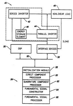
FIGURE 5 depicts the digital and analog components
associated with a preferred embodiment of the invention.
FIGURE 6 depicts an analog embodiment of the digital
components of the apparatus of Figure 5.
WO94/10743 214 ~ 9 8 7 PCT/US93/09~3
-
FIGURES 7A-7E depict the processing of a waveform in
accordance with the present invention.
Like reference numerals refer to corresponding parts
throughout the several views of the drawings.
Detailed Descri~tion of the Invention
Figure 5 depicts an active power line conditioner 40 which
includes a series inverter 42 which is coupled to a parallel
inverter 44 through an energy storage element 46, such as a
dc link. The active power line conditioner 40 is used to
condition power which is delivered to nonlinear load 48. In
a preferred embodiment of the invention, digital circuitry
is used to derive a feed-forward load current flln~mental
signal which may be subsequently processed and used as a
reference signal for the parallel inverter 44.
In particular, the preferred embodiment of the invention
includes a Digital Signal Processor (DSP) 50 which is
coupled through a bus 52 to a memory unit 54, which may be
any combination of RAM, ROM, or other memory medium. The
DSP 50 is also coupled to interface devices 56. As used
herein, interface devices 56 include analog-to-digital
converters, digital-to-analog converters, pulse width
modulators for the respective inverters, and may include
keyboards, monitors, printers, and other equipment to
provide an interface between a user of the digital equipment
tDSP and Memory), and an interface between the digital
equipment and the analog components (series inverter 42,
energy storage element 46, parallel inverter 44).
The interaction between a DSP 50, a memory unit 54, and
interface devices 56 is known in the art. The preferred
embodiment of the present invention is directed toward
execution of the program modules within the memory unit 54.
In particular, as will be described below, DSP 50 executes
a number of program modules including: an initialization
WO94/10743 2~4~9~ PCT/US93/09343
-12-
module 58, a direct component processor 60, a quadrature
component processor 62, a fl~n~m~ntal signal constructor 64,
and a fundamental signal processor 66. In short, these
modules process the load current signal (Iload) to determine
the load current fundamental. Once the load current
fundamental signal is identified, it can be subtracted from
the instantaneous load current to derive a load current
harmonic signal which can be-applied as a reference signal
through the interface devices 56 to the parallel inverter
44, thereby improving the quality of the voltage signals
applied to the nonlinear load 48.
In accordance with the invention, the derivation of the load
current fundamental signal can be realized in one cycle.
The load current fundamental signal is multiplied by
specified components of cosine and sine reference signals to
divide it into direct and quadrature signals. The direct
and quadrature signals are proportional to the amplitude of
the specified components of the reference signals at the
specified phase. Each cycle of the direct and quadrature
signals is sampled a number of times to form direct and
quadrature signal segments. The direct and quadrature
signal segments are respectively placed in direct and
quadrature circular buffers. Each circular buffer includes
a number of formerly sampled segments. Before adding a new
segment, the oldest segment in the buffer is dropped.
Direct and quadrature amplitude values, corresponding to the
sum of all sampled segments within the respective circular
buffers, are maintained. The buffers act as an averaging or
integrating filter for the segment amplitude values. The
instantaneous direct and quadrature amplitude values are
respectively re-multiplied by the same specified components
of the cosine and sine signals to produce in-phase direct
and quadrature fundamental signal components. These signals
are then added to form a vector sum constituting the one-
cycle delay load current f~]n~mPntal signal (with properphase and amplitude).
W O 94/10743 1 2 1 ~ 6 9 8 7 PC~r/US93/09343
-
These processing steps may be realized with the digital
apparatus of Figure 5. The individual processing components
of the invention are disclosed in the form of pseudo code.
The initialization module 58 serves to clear variables, and
later increment variables. As suggested by the description
; in the previous paragraph, a number of constants and
variables are associated with the method of the invention.
First, the number of elements within the circular buffer
must be defined. This number is equivalent to the sampling
rate. As used herein, this constant will be defined as "k~'.
The particular harmonic of interest must also be identified.
That is, the invention may be used to reconstruct the
fundamental load current signal or any harmonic within the
load current. The individual harmonic value will be
identified as "n".
A variable must also be defined for the instantaneous direct
sampled segment of the load current signal. This variable
is a "sliding" term in the sense that it repeatedly moves,
or slides, through the circular buffer. The direct
component is obtained by multiplying the load current by
specified components of a cosine reference sigr.al.
Therefore, this variable will be defined as
"cosine_sliding_window[i]". Through similar reasoning, the
quadrature component variable will be defined as
"sine_sliding_window[i]".
Variables for storing the direct and quadrature buffer sum
amplitudes are also required. These variables will be
respectively denominated "cosine_total" and "sine_total".
Thus, the foregoing variables are initialized through the
initialization module 58. In particular, the initialization
module may be formed as follows:
(a) for i:=O to k do
(b) begin
(c) cosine_sliding_window[i]:= O;
(d) sine_sliding_window[i]:= 0;
(e) end
W094/107~ 4~9~ -14- PCT/US93/09343
(f) cosine_total:= 0;
(g) sine_total:= 0;
The constant values may also be defined in the
initialization module. The next component associated with
the invention is the direct component processor 60, which
may be defined in pseudo code as follows:
(h) cosine_total:= cosine_total-
cosine_sliding_window[i]
(i) cosine_sliding_window[i]:=
cos(2*~*n*i/k)*input_signal
(j) cosine_total: cosine_total +
cosine_sliding_window[i]
As previously discussed, a circular buffer is maintained
which includes a sum of former signal segment values. In
order to enter the new signal segment value into the buffer,
a former signal segment must be eliminated from the buffer.
Line (h) of the foregoing code achieves this function.
The former value is then overwritten by an instantaneous
signal value, as performed by line (i). In particular, the
input_signal, or load current signal, is multiplied by a
specified component of a cosine reference signal. The
specified component of the cosine reference signal is
identified by the harmonic term "n". In addition, the
cosine value includes a fractional value corresponding to
its position in the rotational buffer, as indicated by the
"i/k" term. Recall, that the "i" term denotes the
instantaneous position in the buffer, while the "k" term
denotes the total buffer size.
The final line of the pseudo code, line (j), performs the
task of updating the buffer sum value. In other words, the
new instantaneous amplitude value is added to the buffer sum
value (cosine_total).
The quadrature component processor 62 operates in an
analogous manner; except a sine term is utilized. Thus, the
WO94/10743 214 6 9 8 7 PCT/US93/09343
-15-
quadrature component processor 62 may be characterized as
follows:
(k) sine_total:= sine_total-
sine_sliding_window[i]
(1) sine sliding_window[i]:=
- sin(2*~*n*i7k)*input_signal
~ (m) sine_total: sine_total +
sine_sliding_window[i]
The fundamental signal constructor 64 is invoked at this
juncture. The fundamental signal constructor 64 is used to
generate the output signal. The output signal may be
generated by the following computation:
(n) output_signal := (cos(2*~*n*i/k)*cosine_total +
sin(2*~*n*i/k)*sine_total)/k
As the code indicates, the previously defined cosine_total,
or amplitude term, is multiplied by specified components of
a cosine reference signal. Thus, the instantaneous cosine
reference signal, in proper phase, is being multiplied by an
averaging or integrating buffer value, to provide a proper
amplitude term. The same action is performed for the sine
signal. The respective products are then added to form a
vector sum. The sum of the products is then divided by the
buffer size to provide an instantaneous signal corresponding
to one sample value (a value corresponding to the "i" term
of the buffer).
In sum, the frequency component of interest of the load
current input signal is divided into direct and quadrature
signals. Bach cycle of the direct and quadrature signals is
subjected to multiple sampling. The samples are summed and
placed in a circular buffer. Subsequently, these values are
updated as new signals are processed. The amplitude sum of
the buffer values is used as an averaging term in subsequent
processing. In particular, specified components of
instantaneous cosine and sine signal segments are
respectively multiplied by the cosine buffer and sine buffer
~, ~69~ ~
WO94/10743~ PCT/US93/09343
-16-
sum values. Thus, the buffer values provide a proper
amplitude value, while the reference signal provide a proper
phase value for the load Furrent signal.
In this way, the load current fundamental signal is
efficiently derived, within one cycle, with minimal
computing power. Note also that unwanted frequencies are
clearly eliminated with the method of the invention.
Fundamental signal processor 66 then performs a simple
operation on the derived load current fundamental signal:
(o) parallel_reference:= input_signal -
output_signal
This code merely subtracts the derived load current
fundamental signal from the input signal to render a
harmonic ripple signal (parallel_reference) which is used as
a reference signal for the parallel inverter 44.
Naturally, the foregoing code is re-executed for as long as
a signal needs to be processed. However, prior to re-
entering the code at line (h), it is necessary to perform
some additional initialization tasks. In particular, the
initialization module 58 preferably includes the following
code:
(p) i:= i + 1
(q) i:= i mod k
The "i" term is incremented and then divided by the buffer
size "k". As the "mod" command indicates, the "i" term will
assume the remainder of this division. Consequently, a
circular buffer is maintained.
The digital embodiment of the invention has been practiced
by sampling an input signal every 69.4 microseconds and
placing the sampled values within a 240 element buffer. The
2146987
W O 94/10743 PC~r/US93/09343
- -17-
instantaneous cosine and sine signal values were obtained
through a look-up table.
The nature of the invention is more fully appreciated with
reference to Figure 6, which depicts an analog embodiment of
the invention. The roughly equivalent digital elements are
indicated in phantom.
The analog operation of the invention is as follows. The
input signal is respectively multiplied by cosine and sine
terms through multipliers 70. A one fundamental cycle
delayed version of the output of each multiplier 70 is
produced by phase-shift elements 72. The one fundamental
cycle delayed signals are subtracted from the present value
of the signal at adders 74. The outputs of adders 74 are
respectively processed by integrators 76. The integrators
76 provide a smoothed or averaged output signal. The
resultant signals are re-multiplied by the instantaneous
cosine and sine signals through multipliers 78 to provide
proper phase terms. The resultant products are summed by
adder 80 to yield the load current fundamental signal, IfUnd~
The load current fundamental signal, IfUnd~ is subtracted at
adder 82 from the instantaneous load current, Iload, to
produce a load current ripple signal, Iripple, which may be
used by the parallel inverter 44.
The signal processing of the invention is graphically
depicted in relation to Figures 7A-7E. Figure 7A depicts an
input signal which is respectively multiplied by the cosine
and sine reference signals of Figure 7B. The wave- forms of
Figure 7C represent the direct and quadrature signals
respectively generated by the direct component processor 60
and quadrature component processor 62. The waveforms of
Figure 7D correspond to the output of multipliers 78A. The
waveform of Figure 7E is the sum of the waveforms of Figure
7D; that is, it is the fundamental load current signal.
(The waveforms of Figures 7C-7E are exaggerated for
illustrative purposes).
W094/10743 2~ 469~ -18- PCT/US93/09343
The foregoing descriptions of specific embodiments of the
present invention are presented for purposes of illustration
and description. They are not intended to be exhaustive or
to limit the invention to the precise forms disclosed,
obviously many modifications and variations are possible in
view of the above teachings. The embodiments were chosen
and described in order to best explain the principles of the
invention and its practical applications, to thereby enable
others skilled in the art to best utilize the invention and
various embodiments with various modifications as are suited
to the particular use contemplated. It is intended that the
scope of the invention be defined by the following Claims
and their equivalents.