Language selection

Search

Patent 2147196 Summary

Third-party information liability

Some of the information on this Web page has been provided by external sources. The Government of Canada is not responsible for the accuracy, reliability or currency of the information supplied by external sources. Users wishing to rely upon this information should consult directly with the source of the information. Content provided by external sources is not subject to official languages, privacy and accessibility requirements.

Claims and Abstract availability

Any discrepancies in the text and image of the Claims and Abstract are due to differing posting times. Text of the Claims and Abstract are posted:

  • At the time the application is open to public inspection;
  • At the time of issue of the patent (grant).
(12) Patent: (11) CA 2147196
(54) English Title: MICROWAVE INTEGRATED TUNED DETECTOR
(54) French Title: DETECTEUR HYPERFREQUENCE ACCORDE
Status: Deemed expired
Bibliographic Data
(51) International Patent Classification (IPC):
  • G01R 21/01 (2006.01)
  • G01R 21/12 (2006.01)
  • H01Q 9/04 (2006.01)
  • H01Q 23/00 (2006.01)
(72) Inventors :
  • OPREA, ALEXANDRU (Canada)
(73) Owners :
  • KASTEN CHASE APPLIED RESEARCH LIMITED (Canada)
(71) Applicants :
(74) Agent: SIM & MCBURNEY
(74) Associate agent:
(45) Issued: 2002-11-19
(22) Filed Date: 1995-04-18
(41) Open to Public Inspection: 1995-11-10
Examination requested: 2002-03-19
Availability of licence: N/A
(25) Language of filing: English

Patent Cooperation Treaty (PCT): No

(30) Application Priority Data:
Application No. Country/Territory Date
08/239,454 United States of America 1994-05-09

Abstracts

English Abstract


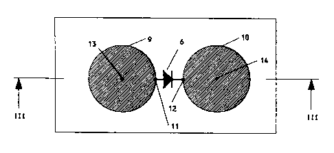
A microwave detector, which integrates two circular
patch antennas with a detector diode. The high impedance
at the edge of the circular patch antenna is combined
with 180° out of phase electric fields at diametrically
opposite points, so as to match to the RF impedance of a
zero or small DC bias diode. The result is a very
simple, high-sensitivity narrow-band microwave integrated
detector.


Claims

Note: Claims are shown in the official language in which they were submitted.


5

I CLAIM

1. A microwave integrated tuned detector for
receiving microwave signals in a predetermined frequency
range, comprising:
a) a DC output;
b) a substrate;
c) a grounded plane mounted on one side of said
substrate;
d) at least two circular patch antennae mounted
on an opposite side of said substrate from said grounded
plane, said antennae being of predetermined radius for
exciting a dominant TM11 mode in said predetermined
frequency range;
e) a detector diode having one terminal thereof
connected to one of said at least two circular patch
antennae, and having an opposite terminal thereof
connected to the other of said at least two circular
patch antennae;
f) a centre point of said one of said at least
two circular patch antennae being connected to said
grounded plane for providing a DC return path for said
detector diode; and
g) a centre point of said other one of said at
least two circular patch antennae being connected to said
DC output.

2. The microwave integrated tuned detector of
claim 1, wherein said detector diode is a Schottky diode.

3. The microwave integrated tuned detector of
claim 2, wherein said Schottky diode is unbiased.

4. The microwave integrated tuned detector of
claim 2, wherein said Schottky diode is biased at a small
DC current.

6
5. The microwave integrated tuned detector of
claim 1, wherein said detector diode is connected to
respective edges of said at least two circular patch
antennae.

Description

Note: Descriptions are shown in the official language in which they were submitted.


214719~


MICROWAVE INTEGRATED TUNED DETECTOR

Field of the Invention
This invention relates in general to microwave tuned
detector-receivers, and more particularly to a low-cost,
high-sensitivity microwave tuned receiver which
integrates at least two circular patch ant~nnAs with a
detector diode.
Background of the Invention
Traditional microwave detector designs use resistive
terminations to match an RF source. However, the
detector diodes used in such designs, when operated
unbiased or at a small DC bias, have a relatively high RF
resistance and receive only a small fraction of the
available signal power when connected in parallel to the
resistive termination (e.g. a 50 ohm resistor).
In narrow band applications, high sensitivity tuned
detectors are preferred. Impedance transformation and
reverse-phasing of the detector diode terminals have been
used to increase the sensitivity and output voltage of
the resistive termination used in such prior art designs.
Nevertheless, both ter-hniques have deficiencies. The
first technique makes use of circuit elements such as
quarter-wave high impedance transmission lines, which are
difficult to achieve with conventional lines. The second
ter~;gue requires a 180 power divider. The requirement
for additional elements to implement these two prior art
tec~nique~ increases the complexity and size of the
detector assembly and introduces extra losses.
Summarv of the Invention
In accordance with the present invention, two
closely separated circular patch antennae are provided
for receiving the microwave signal. A detector diode is
placed in between the two antennae and is connected to
their respective adjacent edges. The centre of one
antenna is grounded to provide the DC return path for the
diode. The centre of the second antenna provides the DC

2l ~7196


output of the detector.
The integrated tuned detector embodying the present
invention takes advantage of both prior art techniques
without requiring the use of additional elements. The
re~ult is a very simple, high-sensitivity integrated
tuned detector.
The detector of the present invention has the
following improvemQnts over prior art tuned detectors:
(1) It combines the input power from two antennae
resulting in a 6dB increase in output voltage.
(2) It provides a certain degree (dep~ ng on antenna
separation) of spatial diversity;
(3) It doe~ not need circuit elements to filter out the
high frequency component at the output of the detector;
(4) It doe~ not need circuit elements to provide a DC
path for the diode.
Further advances of the microwave detector embodying
the invention will be more fully understood from a
consideration of the following detailed description in
conjunction with the accompanying drawings.
Brief Descri~tion of the Drawinqs
In the drawings:
Figure 1 i~ an equivalent functional diagram of a
high-sensitivity integrated tuned detector according to
well known design;
Figure 2 shows an implementation on microstrip of an
integrated tuned detector according to the present
invention;
Figure 3 i~ a cross-section through the lines III-
III in Figure 2; and
Figure 4 shows an alternative embodiment in which
circuitry for performing polarization diversity has been
added.
Detailed Descri~tion of the Preferred Embodiment
Figure 1 shows the equivalent functional diagram of
a high-sensitivity integrated detector. The antenna 1
receives the microwave signal. The power spliter 2

214719fi


divides the input power evenly and applies it to the
impe~co transformers 3 and 5, with a 180 phase
difference. The impedance transformer 3 raises the
impedance to as high a value as is practical and feeds
the anode of a Schottky barrier detector diode 6. The
impe~nss transformer 5 provides the same function as the
impedance transformer 3 and supplies the cathode of the
diode 6. The high freguency component of the detected
signal is removed by low-pass filter 7. The inductor 4
provides the DC return path for the diode 6.
These functions may be implemented very simply
through the exploitation of well known patch antenna
teçhnology.
Figures 2 and 3 show an implementation on microstrip
of these functional blocks according to the present
invention.
A pair of circular patch antennae 9 and 10 are
disposed on a substrate 15, having a ground plane 16 on
the opposite side from the antenna patches 9 and 10. The
radius of both circular patch antennae 9 and 10 is
calculated to excite the dominant TM~1 mode at any
frequency of intQrest. For this mode, the electrical
field is zero at the centre of the patch. However, at
diametrically opposite points on the circumference of the
patch the electric fields are 180 out of phase. In
addition, the impedance at the edge of each patch is very
high (i.e. hundreds of ohms.). Further exploiting this
knowledge, it is clear that the signals at points 11 and
12 are 180 out of phase (functional block 2 in Figure 1).
Furthermore, because of the high impedance at points 11
and 12, impedance transformation (functional blocks 3 and
5 in Figure 1) is performed by the antennae themselves.
The electrical field is zero at the centre point 13
of the antenna 9 and therefore it can be grounded to
provide the DC return path for the diode 6 (the function
of the inductor 4 in Figure 1).
The DC output ~ignal i~ present at point 14.

2147191~


Because the field is zero at this point as well, low-pass
filtration (block 7 in Figure 1) is performed by antenna
10. The DC return point 13 and DC output point 14 can be
interchanged, thereby producing a DC output with reverse
polarity.
Accordingly, the configuration of the present
invention results in a high-sensitivity integrated tuned
detector utilizing only three elements.
Alternative variations are possible. In Figure 4 an
example of an integrated tuned detector i8 shown with
polarization diversity. The configuration is essentially
a combination of two orthogonal integrated tuned
detectors in accordance with the present invention (i.e.
by including an additional circular patch antenna 18 with
grounded centre 19, and connected to antenna 10 via an
additional diode 17). The two detectors of Figure 4
share the antenna 10, which also act~ as diversity
combiner.
All ~uch alternative variations are believed to be
within the sphere and scope of the present invention as
defined by the claims appended hereto.

Representative Drawing
A single figure which represents the drawing illustrating the invention.
Administrative Status

For a clearer understanding of the status of the application/patent presented on this page, the site Disclaimer , as well as the definitions for Patent , Administrative Status , Maintenance Fee  and Payment History  should be consulted.

Administrative Status

Title Date
Forecasted Issue Date 2002-11-19
(22) Filed 1995-04-18
(41) Open to Public Inspection 1995-11-10
Examination Requested 2002-03-19
(45) Issued 2002-11-19
Deemed Expired 2008-04-18

Abandonment History

There is no abandonment history.

Payment History

Fee Type Anniversary Year Due Date Amount Paid Paid Date
Application Fee $0.00 1995-04-18
Registration of a document - section 124 $0.00 1995-10-26
Registration of a document - section 124 $0.00 1997-03-06
Maintenance Fee - Application - New Act 2 1997-04-18 $100.00 1997-03-21
Maintenance Fee - Application - New Act 3 1998-04-20 $100.00 1998-02-19
Maintenance Fee - Application - New Act 4 1999-04-19 $100.00 1999-03-08
Maintenance Fee - Application - New Act 5 2000-04-18 $150.00 2000-03-28
Maintenance Fee - Application - New Act 6 2001-04-18 $150.00 2001-03-30
Maintenance Fee - Application - New Act 7 2002-04-18 $150.00 2002-02-14
Request for Examination $400.00 2002-03-19
Final Fee $300.00 2002-09-05
Maintenance Fee - Patent - New Act 8 2003-04-22 $150.00 2003-04-22
Maintenance Fee - Patent - New Act 9 2004-04-19 $200.00 2004-04-15
Maintenance Fee - Patent - New Act 10 2005-04-18 $250.00 2005-03-30
Maintenance Fee - Patent - New Act 11 2006-04-18 $250.00 2006-04-04
Owners on Record

Note: Records showing the ownership history in alphabetical order.

Current Owners on Record
KASTEN CHASE APPLIED RESEARCH LIMITED
Past Owners on Record
DISYS CORPORATION
OPREA, ALEXANDRU
Past Owners that do not appear in the "Owners on Record" listing will appear in other documentation within the application.
Documents

To view selected files, please enter reCAPTCHA code :


To view images, click a link in the Document Description column. To download the documents, select one or more checkboxes in the first column and then click the "Download Selected in PDF format (Zip Archive)" or the "Download Selected as Single PDF" button.

List of published and non-published patent-specific documents on the CPD .

If you have any difficulty accessing content, you can call the Client Service Centre at 1-866-997-1936 or send them an e-mail at CIPO Client Service Centre.


Document
Description 
Date
(yyyy-mm-dd) 
Number of pages   Size of Image (KB) 
Representative Drawing 2002-05-16 1 21
Abstract 1995-04-18 1 12
Cover Page 1995-04-18 1 15
Description 1995-04-18 4 162
Claims 1995-04-18 2 41
Drawings 1995-04-18 2 60
Representative Drawing 1998-06-18 1 16
Cover Page 2002-10-17 1 45
Prosecution-Amendment 2002-03-19 1 58
Fees 2002-02-14 1 62
Assignment 1995-04-18 57 2,812
Fees 2003-04-22 1 50
Correspondence 2002-09-05 1 51
Fees 2000-03-28 1 51
Fees 2001-03-30 1 50
Fees 2004-04-15 1 51
Fees 2005-03-30 1 53
Fees 2006-04-04 1 54
Fees 2007-06-21 2 204
Fees 1997-03-21 1 56
Fees 1997-04-30 2 68