Note: Descriptions are shown in the official language in which they were submitted.
21~7~
Title: METALLIC BODY Wl~ VAPOR-DEPOSITED TREATMENT
LAYER(S) AND AD~IESION-PROMOTING LAYER
Technical Field
This invention relates to metallic bodies, and more particularly, to
s metal foils such as copper foils. The metal bodies have at least one vapor-deposited
treatment layer overlying at least one side thereof, and a layer of an adhesion-promoting material overlying at least one treatment layer. These foils are useful in
the manufacture of a variety of products including batteries, EMI/RFI shielding
gaskets and panels, and printed circuit boards (PCBs).
BackEround of the ~nvention
The present invention relates to the surface treatment of metal bodies,
and more particularly, to metal foils such as copper foils which are used in theproduction of a variety of products including printed circuit boards. More
particularly, the invention relates to surface treatments for improving the properties
of metallic bodies such as copper foils to maintain a bright copper tone during long
storage and throughout lamination procedures conducted under heat and pressure
while at the same time retaining the solderability and/or solder-wettability of the
surface of the copper foil.
Printed circuit boards are currently used as the substrate materials in
a wide variety of electronic devices. Typically, these boards are fabricated from a
2 1 ~ 7 ." 3 i~
thin sheet of copper foil laminated to either a fiberglass/epoxy hard board or, in some
instances, flexible plastic substrates. During the latter stages of the fabrication, the
copper foil is printed with the necessary circuit pattern, and the unnecessary portions
of the copper foil are then etched away to provide the desired interconnecting
circuitry between various components in the electronic circuit design.
Copper foils used in such applications are prepared genera11y either by
electrolytic deposition or a rolling technique. When the copper foil is producedelectrolytically, the copper foil contains a matte or rough side and a shiny side. The
side laminated to the plasdc substrates generally is the matte side. Whether
electrolydcally formed copper foil or rolled copper foil is used, the surface of the
foils thus formed are not readily amenable to the producdon of adequate bond
strength after lamination. Therefore, the foil must be treated by addidonal chemical
processes to improve its properdes including bondability to resin surfaces, oxidation-
resistance, corrosion-resistance, etc. The shiny side of the copper foils are treated
to prevent oxidation during storage or lamination under heat and pressure. Various
techniques have been suggested and udlized to improve the adhesion of the matte side
of the copper foil to various polymeric substrates. One such practice for achieving
adhesion between copper foil and insulating polymeric substrates has been to roughen
the copper surface.
Surface roughening has been achieved by several means. The
electrodeposited copper foils can be electroforrned with a rough surface. On top of
this rough surface further roughening is carried out by applying a high surface area
treatment. These treatments may be a copper deposited electrolytically in nodular or
powder form, or a copper oxide which grows nodular or dendritic, among others.
Often times the rolled copper foil has mechanical roughness imparted to it during
rolling or by subsequent abrasion. The rolled foils also are conventionally treated
with surface area increasing nodular copper or copper oxide treatments.
These surface roughening treatments increase adhesion to the polymers
by ~orming a mechanical interlock with the resin. The mechanical interlock is formed
when an adhesive in its liquid state is applied and then cured or when the resin melts
,.. ,- .. - ,~........... ,, . , , .. : . . . , . ,, ... , ,, . ~-.- , -
-` - 2i~7~3l~
and flows priOT to cure during larnination. The polymers flow around the roughened
surface area treatments to forrn the mechanical interlock.
There are several factors contributing to the adhesion measured
between the copper foil and the polymeric resin. Some of these are surface area, type
S of Ioughness, wettability, chemical bond formation, type of chemical bond, formation
of interpenetrating networks, and properties of the adhering materials.
During an adhesion test the interlocked resin and copper often adhere
well enough that failure occurs wi~hin the resin, a cohesive failure. With some resins
the mechanical interlocking of treatment and resin does not result in the desired high
adhesion and failure occurs at the interface between resin and copper, an adhesive
failure.
The surface roughening that has been used to enhance adhesion
between copper and polymeric resin substrates may cause difficulties in the
manufacture of PCBs and contribute to poor PCB performance. In the subtractive
lS copper etching process additional etching time is required to remove the dendrites or
nodules embedded in the resin. Fhis not only slows down the production process but
contributes to greater line loss due to the lateral etching of the copper line's sidewalls.
The surface roughening contributes to poor PCB electrical performance by degrading
high frequency electrical signals. The necessity of having a rough base foil haslimited other properties, such as tensile strength and elongation, that produce good
laminate and PCB performance. The dendritic or nodular surface roughening
treatments are difficult to apply, requiring special equipment in the case of electrolytic
treatment, and special chemicals in the case of the oxide treatments.
The bonding strength of the foils to the polymeric substrates can also
be improved by coating the foils with materials which are capable of enhancing the
adhesion between the foil and the polymeric substrates. Various materials have been
suggested in the literature as adhesion-promoting compounds, and these include
organic materials such as phenol resins, epoxy resins, urethanes, silanes, polyvinyl
butyral resins, etc. It also has been suggested to deposit layers of various metals and
` ` 21~73.3ll
metal alloys to improve the adhesion between the copper foil and the polymeric
substrates.
U.S. Patent 3,585,010 a,uce et al) describes a conductive element for
a printed circuit board comprising a copper foil and a metallic barrier layer which
substantiaUy reduces the staining of printed circuit boards. The metallic layer is a
thin deposit of a metal selected from the group consisting of zinc, indium, nickel,
cobalt, tin, brass and bronze. The barrier layer is applied to one side of the copper
foil by standard electrodeposition procedures pertaining the particular metallic layer.
The patentees also suggest that the metallic barrier layer does not have to be
electrodeposited on the surface of the copper foil but may be applied by other means
such as vapor deposition. After deposition of the barrier layer, the foil may be given
additional treatments prior to lamination such as with a corrosion-inhibiting agent.
U.S. Patent 4,268,541 akeda et al) describes a process for producing
a material having a vapor-deposited metal layer useful particularly in forming
resording materials. The process described in this patent comprises vapor depositing
a layer of metal, a layer of different metals in contact with each other, a layer of a
metal alloy, a layer of a metal and a metal compound in contact with each other or
a layer of a metal compound as the metallic layer on a support or substrate which
may be a polymeric material, a composite of a polymeric material and paper, woven
or non-woven cloth or paper. Subsequent to the formation of a layer by vapor
deposition, a second layer of an organic material is applied over the metallic layer by
vapor deposition using an evaporable organic material. The layer of organic
compound over the metal layer serves as a buffering ]ayer for the metallic layer and
renders the metallic layer formed by vapor deposition more slippable.
U.S. Patent 4,383,003 (Lifshin et al) and its divisional U.S. Patent
4,455,181 describe copper-clad laminates useful in preparing high resolution printed
circuit patterns. Laminates are made by vapor depositing a film of zinc on a vapor~
deposited copper film which is on a silica-coated aluminum carrier sheet, vapor
depositing a silica film on the resulting zinc-copper foil, bonding the resulting body
to a substrate, and then stripping the silica-coated aluminum carrier sheet from the
2 ~ 7 ~ ~ ~
copper clad laminate. One of the laminated products described in the '003 patentcomprises a thin copper sheet, an ultra-thin film of zinc vapor-deposited on said
copper sheet and a film of silica or alumina vapor-deposited on said zinc film.
Optionally, a coating of a silane coupling agent is deposited over the silica film.
S Summarv of the Invention
This invention relates to a metal body having at least one vapor-
deposited treatment layer overlying and adhered to at least one side of the metal body,
and a layer of adhesion-promoting material overlying and adhered to at least onetreatment layer, provided that when two treatment layers are deposited on one side
of the body and the first layer is vapor-deposited zinc, the second layer is not vapor-
deposited silica or alumina, said adhesion-promoting material being suitable forenhancing adhesion between said body and another substrate. The invention also
relates to laminates comprising: a metal foil and at least one vapor-deposited
treatment layer overlying and adhered to at least one side of the metal foil; a layer
of adhesion-promoting material overlying and adhered to the at least one vapor-
deposited treatment layer; and a layer of an electrically non-conductive material
overlying and adhered to the adhesion-promoting layer.
Brief Description of the Drawings
Fig. 1 is a schematic diagram representing a cross-sectional view of a
metal foil of the present invention including one vapor-deposited layer and one
adhesion-promoter layer.
Fig. 2 is a schematic diagram representing a cross-sectional view of
another metal foil of the present invention.
Fig. 3 is a schematic diagram representing a cross-sectional view of
another metal foil according to the present invention.
Fig. 4 is a schematic diagram representing a cross-sectional view of
another metal foil according to the present invention.
Fig. 5 is a schematic diagram representing a cross-sectional view of
another metal foil according to the present invention.
21473~
-6-
Fig. 6 is a schematic diagram representing a cross-sectional view of
another metal foil according to the present invention.
D~scription of the Preferrç~Embodiments
Metal Bodies.
S The metal bodies which can be utilized and treated in accordance with
the present invention are preferably electrically conductive metal bodies. The choice
of metal body will depend upon the desired end use of the metal body.
The metal bodies utilized in the present invention may be of any
configuration such as metal sheets, bars, rods, wires, foils, etc. Preferably, the metal
body is a foil, more particularly, a copper or copper-based alloy foil. Accordingly,
the discussion within the specification generally will be directed to foils, and more
particularly, copper foils, although the general discussion should be understood to be
applicable to other foils and metal bodies.
Copper and copper-based alloy foils are well known in the art and are
made by various techniques. Wrought or rolled foil is produced by mechanically
reducing the thickness of a metal (copper) or alloy (copper alloy) strip or ingot by a
process such as rolling. Electrodeposited foil is produced by electrolytically
depositing copper ions on a rotating cathode drum and then peeling the deposited strip
from the cathode. This procedure can be used to form continuous strips of the foil
Foils can also be prepared by other procedures. For example, a copper foil can be
prepared by electrodepositing or vapor depositing a layer of copper on a conductive
carrier such as aluminum. Another copper foil can be prepared by rolling a copper
layer onto an alloy foil such as an iron-nickel alloy. The copper can be rolled onto
one or both sides of the iron-nickel alloy. Yet another example of a multilayer foil
is a molybdenum foil or layer coated on both sides with copper. Altematively,
copper can be vapor-deposited on a release coated carrier, and thereafter the vapor-
deposited film of copper can be removed from the release-coated carrier.
Electrodeposited and rolled or wrought copper foils are preferred, and
electrodeposited copper foils are especially preferred. The copper foils typically have
nominal thicknesses ranging from about 0.0002 inch ~o about 0.02 inch. Foil
';'' :.'',''''.~.'
'''~''.', ,'-
21~73~
thickness is sometimes expressed in terms weight and typically the foils of the present
invention have weights or thicknesses ranging from about l/8 to about 14 ozlft2. The
foils used as the base foil in this invention may be as-plated foils or annealedelectrodeposited foils. The wrought copper foils may be as-rolled or annealed
wrought copper foils.
Electrodeposited coppcr foils have a smooth or shiny (drum) side and
a rough or matte (copper deposit growth front) side. The treatment layers described
more fully below can be adhered to either side of the foil and in some instances are
adhered to both sides.
In one embodiment, the side or sides of the foil (electrodeposited or
wrought) to which the treatment layer is adhered is a "standard-profile surface,"
"low-profile surface" or "very-low-profile surface." The term "standard-profile
surface" is used herein to refer to a foil surface having an R~", of about lO ILm or less.
Standard profile electrodeposited copper foil also may be characterized as having a
columnar grain structure of preferred orientation and high densities of crystal defects
such as discolorations and twin boundaries, and the foil has an average grain size of
up to about 20 microns. The term "low-profile surface" refers to a foil surface
having an R"" of about 7,~m or less. The term "very-low-profile surface" refers to
a foi1 surface having an R,~ of about 4~m or less. R"" is the mean of the maximum
peak-to-valley ver~ical measurement from each of five consecutive sampling
measurements, and can be measured using a Surftronic 3 profilometer marketed by
Rank Taylor Hobson, Ltd., Leicester, England.
When the copper foil products of the present invention are to be used
in PCB applications, it is often desirable that the copper foils have controlled low
profiles to provide etchability and impedance control. It is also preferred that these
foils have high ultimate tensile strengths (UTS) to provide desired handling andsurface quality characteristics, and high elongations at elevated temperatures to resist
cracking. In one embodiment, the copper foils utilized in the present invention are
characterized as being controlled low profile electrodeposited copper foils having a
substantially uniform randomly oriented grain structure that is essentially columnar
- ~ 21~733~
grain-free and twin-boundary-free and has an average grain size of up to about 10
microns. These foils generally have ultimate tensile strength measured at 23 C in the
range of about 70,000 to about 120,000 psi and an elongation measured at 180-C of
about 6% to about 28%. Copper foils h~ving these characteristics may be preparedby the process which comprises (A) flowing an electrolyte solution between an anode
and a cathode and applying an effective amount of voltage across said anode and said
cathode to deposit copper on said cathode; said electrolyte solution comprising copper
ions, sulfate ions, and at least one organic additive or derivative thereof, and the
current density being in the range of about 0.1 to about 5 A/cm2; and (B) removing
the copper foil from said cathode. In one embodiment, the chloride ion concentration
of said solution is up to about 1 ppm.
Such copper foils generally have a matte-side raw foil roughness (R~m)
of 1 to about 10 microns. The R"" for the shiny side of these foils is preferably less
than about 6 microns, and more often in the range of from about 2 to about 5
microns. The weights for these copper foils generally are in the range of from about
1/8 to about 14 ounces per square foot. The foil having a weight of 0.5 ounce per
square foot has a nominal thickness of about 17 microns.
The terms "untreated" and "raw" are used herein to refer to a base foil
as prepared which has not been subjected to subsequent treatment, (e.g., one or more
surface roughening treatments) for the purpose of refining or enhancing the foilproperties. The raw foil is also referred to as "as plated" or "as rolled." The term
"treated" as used herein is used herein to refer to raw or base foil that has been
subjected to at least one such treatment. These treatments are conventional and
typically involve the use of various treating and rinsing solutions. Either or both
sides of the foil can be treated. The treatments may be chemical or physical
treatments.
Various chemicals can be applied to the raw foil to improve the
characteristics of the foil surface. For example, the foil surfaces can be contacted
with an acid such as sulfuric acid to effect microetching of the surface. Also prior
to application of the vapor-deposited treatment layers in accordance with the present
: ~ :
.
': ~
.... . -
. . - - ................................................ ..
- ` 21~7~3~
invention, the copper foils may be electrolytically provided with various metal
coatings such as zinc, tin, copper, chromium or alloys thereof (e.g., chromium-zinc)
by dipping and electroplating techniques well known to those sldlled in the art. For
example, the electroplating of tin or a tin-zinc alloy on the shiny side of a copper foil
is described in U.S. Patent 4,082,591 which is hereby incorporated by reference. In
another example, the raw foil is dipped in an acid solution of chromic acid (CrO3) to
deposit a chromium coating.
Although the foils can be subjected to a surface roughening treatment
prior to the application of at least one vapor-deposited treatment layer, it is a
significant advantage of the invention that improved adhesive characterisdcs for the
foil can be achieved without subjecdng the foil to an added surface roughening
treatment. Thus, in one embodiment of the invendon, the foil used in the invendon
can be raw foil which has been cleaned of surface impurides but is otherwise
characterized by the absence of any added surface roughening treatment on the side
or sides to which the vapor-deposited treatment layer(s) is adhered. The term "added
surface roughening treatment" refers to any treatment performed on a base or raw foil
that increases the roughness of the surface of the foil. These treatments include
chemical treatments such as copper deposited electrolytically in nodular or powder
form, or copper oxide which grows nodular or dendritic. In one preferred
embodiment, the base foil is microetched by dipping in an acid soludon such as a20æ by volume of sulfuric acid in water at about 65 C for about 15 seconds followed
by an immediate water rinse. Other useful surface modification treatments include
glow discharge and sputtering.
In one embodiment, the mechanical roughness imparted to wrought
copper foil during rolling or by subsequent abrasion which increases roughness
beyond that of a standard profile surface is considered to be an added surface
roughening treatment. In another embodiment, any roughness imparted to the raw
or base copper foil that increases the roughness of said foil beyond that of a standard
profile surface is considered to be an added surface roughening treatment. In another
embodiment, any roughness imparted to the raw or base copper foil that increases the
~-. : , . . . -
, . ....................................................... . -
2~73~
-10-
roughness of said foil beyond that of a low-profile surface is considered an added
surface roughening treatment. In another embodiment, any roughness imparted to the
raw or base copper foil that increases the roughness of said foil beyond that of a very
low-profile surface is considered an added surface roughening treatment.
S As indicated above, it is within the scope of the invention to apply the
vapor-deposited treatment layer(s) to foils which have been subjected to an added
surface roughening treatment the treatment. Thus, in one embodiment, one or bothsides of the foil may be treated to provide a roughened layer of copper or copper
- oxide prior to vapor deposition of the treatment layer or layers. The copper can be
deposited electrolytically in nodular or powder form by techniques well known tothose sl~lled in this art. The copper oxide can grow nodular or dendritic. In another
embodiment, the side or sides of the base or raw foil to which the vapor-deposited
treatment layer is adhered is untreated prior to the application of the vapor-deposited
treatment layer to the foil. -
Treatment La~er(sl. ` -
The metal bodies of the present invention have at least one vapor~
deposited treatment layer overlying and adhered to at least one side of the metal body.
As noted above, the vapor-deposited treatment layer may be deposited over raw oruntreated foil, or the treatment layers may be applied to the foil after the foil has been ~ ~ -
subjected to one or more added surface roughening treatments. ~ -
In one embodiment, one side of the foil has a treatment layer, and in
another embodiment, both sides of the foil have a treatment layer. In a further ~ `
embodiment of the invention, one or both sides of the foil may have two or more ` -
consecutive vapor-deposited treatment layers as described more fully below. In yet
another embodiment, the foils of the present invention have at least one roughened
layer of copper or copper oxide between the raw or base foil and the vapor-deposited
treatment layer or layers. ln a further embodiment, the foils of the present invention ;
may have at least one chemically or electrodeposited metal or metal oxide layer on
the foil and between the foil and the one or more vapor-deposited layers.
, .
,1
':
- ` 2147~3~
A variety of vapor-deposited treatment layers may be present on the
foils of the present invention to provide desirable and beneficial properties to the foils
such as stabilization layers, barrier layers, or combinations thereof to prevent or
minimize the appearance of stains and spottings throughout ~he resinous layer when
the foils are used to form printed circuitboards, oxidation-inhibiting layers, moisture-
resistant layers, etc.
1~ one preferred embodiment, the vapor-deposited treatment layer or
~..... ...
. .
layers deposited on one or both sides of the foil is a metallic barrier layer and/or a
metallic stabilization layer. As noted, the invention contemplates the use of more
than one such metallic layers on either or both sides of the foil. The term "metallic"
as applied to the metallic layers useful in the present invention includes metals,
alloys, as well as metal compounds such as metal oxides or nitrides although metals
are preferred.
Examples of metals which may be included in the vapor-deposited
metallic layer include magnesium, aluminum, titanium, chromium, manganese,
copper, bismuth, cobalt, nickel, zinc, indium, tin, molybdenum, silver, gold,
tungsten, zirconium, antimony, chromium-zinc alloy, brass, bronze, and mixtures of
two or more of said metals. When the metallic layers or layers are deposited on the
matte side of an electrodeposited copper foil, the metal is preferably indium, tin,
cobalt, nickel, zinc, copper, manganese, chromium, titanium, bismuth, bronze or
. . .~
zinc-chromium alloy. Preferred metals for the metal layer or layers applied to the ~ ~
~: . .
,
shiny side of an electrodeposited copper foil are those which are etchable and these
include indium, chromium, magnesium, aluminum, copper, tin, nickel, cobalt, zinc: ~. -, ..:
or zinc-chromium alloys.
The foils of the present invention also can contain two or more vapor-
deposited layers on one or both sides of the foil. For example, a first (a barrier
layer) layer of any of the above-identified metals or metal alloys can be vapor- ;~
deposited on the copper foil followed by the vapor deposition of a second layer
(stabilization layer). Alternatively, the second layer may, for example, comprise a
metal oxide such as silica, alumina, indium oxide, magnesium oxide, etc., provided ~-
, i. . ': ~ " : ~ ' ' : , .
21~7t~
that the second vapor-deposited layer does not contain vapor-deposited silica oralumina when the first vapor-deposited layer is zinc.
The thickness of the one or more treatment layers on the metal bodies
of the present invention can be varied, and the desired thickness for any par~cular
S application can be readily determined by one skilled in the art. In general, when a
treatrnent laye~ is a metallic layer, the thickness of the metallic layer may range from
about 10 to about 10,000 A, and in some instances, u~ll be within the range of from
about20 to 1000 A. :
. . -
, .
In anotha embodiment wherein a barrier layer of metal overlies and
is adhered to the base foil, and a metal stabilization layer is vapor-deposited over the ~; -
barrier layer, the thickness of the barrier layer may range from about 0.01 to about
1 micron, and the thickness of the stabilization layer may vary from 0.002 to about ~
0.1 micron. Metals which are particularly useful in the stabilizer layer include tin, - ~ `
nickel, molybdenum, indium, magnesium, aluminum, Zn, Cr and Zn-Cr alloys. ; ~ -
The vapor-deposited treatment layers can be obtained by vapor -~
deposition techniques well known to those skilled in the art, and such techniques ~ ~-
include physical vapor deposition (PVD) which includes thermal evaporation, electron `~
beam deposition, inductive and/or resistive deposition, ion plating, sputtering, plasma-
activated evaporation, reactive evaporation, and activated reactive evaporation; and
chemical vapor deposition (CVD). Physical vapor deposition also has been referred -
to in the literature as vacuum metallization and evaporative coating. In thermal~ ~ -
evaporation deposition procedures, the material to be applied to the metallic body
(generally a metal or alloy) is heated in a high vacuum (e.g., 10-2 to about 10-6 torr)
whereupon the material evaporates or sublimates and travels to the metal object to be
coated. In sputtering processes, energetic inert ions created in a plasma discharge
impact a target and cause the ejection of coating material through momentum
exchange. Physical vapor deposition essentially involves the transfer of the material
and the formation of coatings by physical means alone in contrast to chemical vapor
deposition in which the material transfer is effected by chemical reactions induced by
temperature or concentration gradients between the substrate and the surrounding
.. '
. .. . . . . . . .
.~. . - - .
`` 21~3~
-13-
gaseous atmosphere. The principals of vapor deposition and procedures useful in
vapor depositing various materials including metals is described in Vapor Deposition,
edited by C.F. Powell et al, John Wiley & Sons, Inc., New York, 1966.
Chemical vapor deposition usually is accomplished by vaporizing a
metallic halide and decomposing or reacting the vapors at the foil surface to yield the
non-volatile metal on the surface of the foil as a coating. The chemical reactions of
vapor deposition can be effected by thermal deposition or pyrolysis, hydrogen
reduction, reduction with metal vapors, reaction with the metal foil, chemical
transport reactions, etc. These procedures are described in detail in Chapter 9 of
Vapor Deposition, C.F. Powell, J.H. Oxley, and J.M. Blocker, Jr., editors, J. Wiley
& Sons, Inc., New York, 1966, and this chapter is incorporated by reference for its
description of the CVD processes.
Copper foils having vapor-deposited treatment layers in accordance
with this invention, and in particular, vapor-deposited metallic layers, can be obtained
utilizing an apparatus available from Edwards Coating Systems, identified as E306A.
This unit has an operating vacuum range of from 2 x lo6 mbar to 2 x 10⁻⁵ mbar.
Vapor deposition of metals can generally be accomplished in satisfactory thicknesses
(e.g., about 10 A to 3000 A) in from about 0.3 to about 40 minutes or more at
evaporating currents of from 35 to 80 milliamps. The evaporating current used
depends on the amount and form of the mateAal to be vaporized. For example,
currents of about 65-80 milliamps generally are used to vapor-deposit indium, tin,
chromium, coba!t and nickel. Evaporation currents in the range of 35-50 milliamps
are satisfactory for magnesium and zinc, and currents in the range of 50-65 are
satisfactory for depositions aluminum, manganese, tin and brass. In the Edwards
apparatus the distance from the boat containing the metal to be vaporized to the foil
sample is about 5 inches. In general, thin foil or chips of the coating material are
placed in a tungsten boat and heated under vacuum.
After the treatment layer has been vapor-deposited on the copper foil,
it may be further treated to improve its properties prior to application of the adhesion-
promoting layer. The vapor-deposited metallic layer can be heated to an elevated
.~ ,
2147~
-14-
temperature such as from about 80 C to about 800 C (depending on the vapor-
deposited metal) for a few seconds to one hour to modify the surface coverage,
characteristics and properties of the metallic layer. For example, a metallic layer
such as indium deposited on a copper foil which does not completely cover the copper
S foil leaving about 2 % to 3 % or even 5 % ~Epoæed copper. When the vapor-deposited
indium coating is baked in an oven at an elevated temperature of about l90-C for 60
minutes, the exposed copper concentration of the surface decreases to as little as
0.5%. In another embodiment, the vapor-deposited metal is baked in an oven in anatmosphere of oxygen to convert at least some of the surface metal to the oxide form.
Exposure of the metal surface to nitrogen at an elevated temperature converts at least
a portion of the surface metal to metal nitAde. Heating of the vapor-deposited metal
pAor to application of the adhesion-promoting layer also accelerates the formation of
an alloy of the base metal and the vapor-deposited metal at the base metal-deposited
metal interface.
The properties of the vapor-deposited metallic layer or layers present
in the metal foils of the present invention may be further modified by ion-bombard-
ment/heating, oxygen plasma ion bombardment, and electroplating of the vapor-
deposited metallic layer with materials which improve desirable properties such as
providing oxidation and stabilization protection. For example, the vapor-deposited
metal layer may be electrochemically treated with acidic solutions containing, for
example, chromium, copper, tin, bismuth, or zinc-chromium mixtures, etc., to
deposit chromium, tin, bismuth or zinc-chromium coatings over the vapor-deposited
metal coating to improve properties such as oxidation resistance, etc., prior toapplication of the adhesion-promoting layer.
Adhesion-Promoting Layer.
At least one surface or side of the metal bodies of the present invention
have at least one vapor-deposited treatment layer as described above, and at least one
of the treatment layers has an adhesion-promoting layer overlying and adhered to the
treatment layer. The adhesion-promoting layer is adapted for enhancing the adhesion
between the foil and a substrate such as a polymeric resin substrate used in the
- 2~47~
-15-
formation of PCBs. Depending on the nature of the adhesive or adhesion-promoter
and the intended use of the adhesive layer coated foil, the thichless of this layer may
vary over a wide range from about 4 to about 500,000 A. A wide variety of
adhesion-promoting materhls are known in the art for improving the adhesion of
treated and untreated metal foils to other substrates including polymeric resin
substrates, and such conventional adhesives can be utilized in the present invention.
Improved adhesion is obtained as a result of the coaction between the adhesive and
the vapor-deposited treatment surface or surfaces which have been previously applied
to the metal foil. For electrical purposes, high dielectric strength adhesives are
selected. The adhesives or adhesion-promoters may be organic, organometallic or
inorganic compounds.
In one embodiment, the adhesion-promoting material is an organic
material which may comprise thermosetting or thermoplastic polymers and
copolymers, and mixtures thereof. When organic materials such as thermosetting or
thermoplastic polymers and copolymers are used, they are often referred to in the art
as adhesives, and the thickness of the layer is at the higher end of the range given
above. Generally, thicknesses of from about 10,000 A up to about 500,000 A are
applied over the vapor-deposited treatment layer. In contrast, the organometallic
compounds useful in the adhesion-promoting layer such as the silane coupling agents
are generally referred to as adhesion promoters, and the thickness of the adhesion
promoter is much less, e.g., from about 4 A to about 200 A.
Examples of thermosetting and thermoplastic polymers and copolymers
include epoxy resins, formaldehyde resins, phenol formaldehyde resins, polyesterresins, butadiene and acrylonitrile rubbers, polyvinylbutyral resins, etc. Mixedpoly(vinylbutyral)-phenol-formaldehyde resins also are useful. Various alkyd resins
which are polyesters may be used as adhesive. An example of a useful alkyd resinis a maleic anhydride-ethylene glycol polyester. Such polyesters may be dissolved
in styrene and copolymerized in place under heat with the addition of a small amount
of a peroxide initiator to provide excellent adhesives.
'
. ..
:
` 214~33~
~
In one embodiment, the adhesive material used to form the adhesion-
promoting layer comprises (A) at least one multi-functional epoxy resin. In another
embodiment the adhesion-promoting layer comprises a mixture of epoxy resins -
comprising (A) at least one multifunctional epoxy resin; and (B) a composition
S derived from (B 1) at least one difuncdonal epoxy resin; and (B-2) at least one
component represented by the formula
R~(G)n (I) :, ~
wherein in Formula I, R is an aromatic, alicyclic or heterocyclic group; G is a
functional group selected from the group consisting of COOH, OHSHNH2NHR',
(NHC(=NH))~NH2, R2COOH, R20H, R2SH, R2NH2 and R2NHR', wherein R' is a
hydrocarbon, R2 is an alkylene or alkylidene group, and m is a number in the range
of from l to about 4; and n is a number ranging from 3 up to the number of
displaceable hydrogens on R.
The multifunctional epoxy compounds (A) which can be used alone or
lS in combination with (B) are those containing an average of more than two epoxy
groups (oxirane rings) per molecule. In one embodiment these epoxies contain an
average of up to about six epoxy groups per molecule. In one embodiment the
multifunctiona1 epoxy is an epoxy novolac resin. The multifunctional epoxy can be
a trifunctional or tetrafunctional epoxy resin. (A trifunctional epoxy resin is an epoxy
resin that contains an average of three epoxy groups per molecule, and a tetrafunc-
tional epoxy resin contains an average of four epoxy groups per molecule.) The
multifunctional epoxies typically have average epoxy equivalent weights in the range
of about lO0 to about 250, and in one embodiment from about 190 to about 240. (An
epoxy equivalent weight is the molecular weight of the epoxy molecule divided by the
number of epoxy groups in the molecule. Thus, for example, a trifunctional epoxyhaving a molecular weight of 600 would have an epoxy equivalent weight of 200.)
Examples of commercially available trifunctional epoxy resins that are
useful include Tactix 742 (Dow Chemical) and PT 810 (Ciba Geigy). Examples of
'~'''`''`' '~ " ~' :' ~ : ~ '
.
.. , ~,
2147~3~
-17-
commercially available tetrafi~nctional epoxy resins that are useful include MT 0163
(Ciba Geigy~, Epon 1031 (Shell) and Epon HPT 1071 (Shell).
The epoxy novolacs that are useful include the epoxy cresols and the
epoxy phenol novolacs. E~amples of commercially available novolacs that are useful
S include DEN 438, DEN 439 and Tactix 785 ~each of which is available from Dow),
DPS 164 (Shell) and ECN 1299 (Ciba Geigy).
The difunctional epoxy resin (B 1) can be any difunctional epoxy resin
having an average molecular weight in the range of about 1000 to about 10,000
(epoxy equivalent weight of about 500 to about 5000), and in one embodiment an
average molecular weight of about 1000 to about 6000. (A difunctional epoxy resin
is an epoxy resin that contains an average of two epoxy groups per molecule.) In one
embodiment, a mixture of difunctional epoxy resins is used, one having an average
molecular weight of about 1000 to about 3000, pre~erably about 1500 to about 2500
and the other having an average molecular weight in excess of about 3000 up to about
6000, preferably about 3500 to about 5000.
In one embodiment the difunctional epoxy resin (B-1) is a compound
represented by the formula~
~ R' ~ R'
CHfHCH, ~O~ C--~OCH,CH(OH)C~ O~C ~ OCH,CHCH7 al) ~
O R7 R7 0 .:
wherein in Forrnula (Il), R' and R2 are independently hydrogen or hydrocarbon
groups in the range of I to about 20 carbon atoms, and n is a number in the range
of 1 to about 20, preferably I to about 6, and in one embodiment 1 to about 3, and
in another embodiment 1 or 2. Examples include: bisphenol A wherein R' and R2
are each CH3; bisphenol F wherein R' and R2 are each H; bisphenol AD wherein R'
is H and R2 is CH3. Others include resins wherein: R' is H and R2 is C6H,3; R' is
H and R2 is C,2H25; R' is CH3 and R2 is C2H5; Rl is CH3 and R2 is C4H9; etc.
..., ......................................................... , ,: :-
--` 2147~
`-
-18- ~ -
The compound (B-2) is at least one compound represented by the
formula
R~(G)n (I)
In Formula (I) R is an aromatic, alicyclic or heterocyclic group. G is a functional
S group selected from the group consisting of COOH, OH, SH, NH2, NHR',
~NHC(=NH))mNH2, R2COOH, R20H, R2SH, R2NH2 and R2NHR', wherein R' is a
hydrocarbon group, preferably an alkyl group, of 1 to about 6 carbon atoms, morepreferably 1 to about 3 carbon atoms, and R2 is an alkylene or alkylidene group,preferably an alkylene group, of 1 to about 6 carbon atoms, more preferably 1, 2 or
3 carbon atoms, and m is a number in the range of 1 to about 4 and in one ~i
embodiment m is 2. G is preferably NH2, OH or CH2NH2. n is a number ranging
from 3 up to the number of displaceable hydrogens on R.
The aromatic R groups in Forrnula (I) can be mononuclear, e.g.,
benzene; polynuclear wherein the aromatic nucleus is of the fused type with the
aromatic nucleus being fused at two points to another nucleus, e.g., naphthalene, or
of the linked type wherein at least two nuclei (mononuclear or polynuclear) are linked
through bridging linkages to each other. These bridging linkages can be carbon-to-
carbon single bonds, ether linkages, keto linkages, sulfide linkages, sulfur atoms,
sulfinyl linkages, sulfonyl linkages, alkylene linkages, alkylidene linkages, amino
linkages, etc. Normally the aromatic group R is a benzene nucleus. These aromatic
groups can be alkyl-substituted aromatic groups wherein one or more alkyl groups(e.g., Cl-Clo) are attached to the aromatic nucleus.
The alicyclic R group in Formula (1) can be saturated or unsaturated
and preferably has from 3 to 6 carbon atoms, more preferably 5 or 6 carbon atoms.
These cyclic groups can be alkyl-substituted alicyclic groups wherein one or more ` `~
alkyl groups (e.g., Cl-Clo) are attached to ring carbon atoms. Examples include R
groups derived from cyclopropane, cyclobutane, cyclopentane, cyclopentene, 1,3- ;~
cyclopentadiene, cyclohexane, cyclohexene, 1,3-cyclohexadiene, etc.
-`- 2i4~33`~
-19-
The heterocyclic R group in Formula (I) is preferably derived from a
5- or ~membered nng compound wherein the hetero atom(s) are N, S or O. These
cyclic groups can be alkyl-substituted heterocyclic groups wherein one or more aL~yl
groups (e.g., C,-Clc~) are attached to ring carbon or N atoms. Examples include R
5 - groups derived from pyrrole, furan, thiophene, pyridine, etc.Useful examples of compound (B 2) include o-aminophenol, m-
aminophenol, p-aminophenol, o-phenylenediamine, m-phenylenediamine, ~phenylene
diamine, 1,3-xylylenediamine, isopnoronediamine, 1,3,5-trihydroxy benzene,
diaminodiphenylsulfone, 1,4-xylylenediamine, 3-aminophenylsulfone, 1,4-cyclohex-anediamine, 1 ,3-cyclohexanediamine, l~tolylbiguanide, and mixtures of two or more
thereof.
In one embodiment components (B 1) and (B-2) are merely blended
with each other prior to or at the time of mixing with component (A). In this
embodiment components (B-l) and (B-2) are not pre-reacted with each other. In one
embodiment components (B-l) and (B-2) are pre-reacted with each other prior to
being combined with component (A). This reaction can be effected by contacting
component (B-l) with component (B-2) under reaction conditions until the desiredproduct is obtained. In either case, the ratio of equivalents of (B-l) to (B-2) is
generally from about 1:2 to about 1:4, and in one embodiment from about 1:2.5 toabout 1:3.5. The weight of an equivalent of component (B-l) is determined by
dividing the molecular weight of component (B-l~ by the average number of epoxy
groups per molecule in (B-l). The weight of an equivalent of (B-2) is determined by
dividing the molecular weight of (B-2) by the number of functional groups, G, per
molecule in (B-2). In determining the number of functional groups in (B-2), COOH~
SH~ NHRI~ R2COOH~ R2SH and R2NHRI are each counted as one functional group.
NH2 and R2NH2 are each counted as two functional groups. The number of
functional groups in (NHC(=NH))mNH2 is equal to the number of reactive nitrogen
sites in the group. Thus, for example, when G is NHC(=NH)NHC(=NH)NH2 it is
counted as 6 functional groups.
` ~ 21~7~
-20-
When components (B-1) and (B 2) are pre-reacted with each other the
reaction temperature is gene~ally from about 60 C to about lSO C, and in one
embodiment from about 80 C to about llO C. The time required to complete the
reaction is dependent upon the desired degree of reaction, but is generally from about
2 to about 24 hours, and in one embodiment from about 4 to about 8 hours. In oneembodiment either or both of components (B 1) and (B 2) are dissolved in a suitable
solvent prior to being reacted with each other. E~camples of such solvents include
methylisobutylketone, methyl ethyl ketone, benzene, toluene, acetone, tetrahydro-
furan, etc.
In one embodiment the above-described epoxy adhesive composition
also contains an effecdve amount of a supplemental adduct (C) to enhance the curing
of the epoxy adhesive composition. This supplemental adduct is the reaction product
of at least one difunctional epoxy resin with at least one alkylene polyamine. The
difunctional epoxy resins are the same as the resins (B 1) discussed above. The
alkylene polyamines are compounds represented by the formula
R~-N-(R2-N)n-RI (III)
R' R'
wherein in Porrnula (III), each R' is independently hydrogen or a hydrocarbon group,
preferably alkyl, of 1 to about 10 carbon atoms, preferably 1 to about 4 carbon
atoms; R2 is an alkylene group of preferably 1 to about 4 carbon atoms, more
preferably 2 or 3 carbon atoms; and n is a number in the range of 1 to about 10,preferably 1 to about 4, more preferably 1 or 2. Examples include ethylene diamine,
triethylene tetramine, propylene diamine, trimethylene diamine, etc. The reaction
between the difunctional epoxy resin and the alkylene polyamine is generally carried
out at a temperature of from about 25 C to about lOO C, and in one embodiment
from about 70 C to about 90 C. The time required to complete the reaction is
dependent upon the desired degree of reaction, but is generally from about 2 to about
24 hours, and in one embodiment from about 2 to about 4 hours. In one embodiment
.,.. ~ . . - .
~14733ll
either or both of the reactants are dissolved in a suitable solvent prior to being reacted
with each other. Examples of such solvents include methylisobutyLketone,
methylethylketone, benzene, toluene, acetone, tetrahydrofuran, etc.
The above epoxy adhesive compositions preferably comprise from
S about 10% to about 40% by weight, and in one embodiment about 20% to about 30%
by weight of the multifunctional epoxy (A); from about 40% to about 80% by weight,
and in one embodiment about 55% to about 75% by weight of the composition (B);
and up to about 25 % by weight, and in one embodiment from about 5 % to about 15 %
by weight of the supplemental adduct (C). .
In one embodiment the epoxy adhesive compositions contain an
effective amount of at least one low molecular weight difunctional epoxy compound
to enhance the adhesive characteristics of these compositions. These low molecular ;
weight epoxies typically have molecular weights in the range of about 160 to about
400, and in one embodiment from about 200 to about 250. In one embodiment the
low molecular weight epoxy is represented by the formula ~-
~ O /0
CH2-CH-R'-O-Ar-~R2-CH-CH2 (IV)
.
wherein in Formula (IV), Ar is an aromatic or cycloaliphatic group of the type
discussed above with respect to Formula (I) with the mononuclear groups (e.g., -
benzene) being preferred, and Rl and R2 are independently alkylene or alkylidene -~
groups of preferably 1 to about 6 carbon atoms, and in one embodiment from 1 to
about 3 carbon atoms. An example of a useful low molecular weight difunctional
epoxy is one in which Ar is a benzene nucleus, and R' and R2 are each methylene;this compound being available under the tradename Heloxy 69 from Rhone Poulenc.
These low molecular weight difunctional epoxies are present in the adhesive
compositions at concentrations of up to about 10% by weight, and in one embodiment
up to about 5% by weight. ~ ;~
,~ :
'.
'`.-:. ~. : :
~ ~ . . . .
21~7~
-22-
In one embodiment the epoxy adhesive composition also contains an
effective amount of at least one phenolic resole to enhance the adhesive characteristics
of these compositions. These resoles are typically provided in diluted forrn, the
diluent being a suitable solvent such as ethanol, and having a solids content of, for
S example, about 50% to about 70% by weight. Useful phenolic resoles typically have
gd times of about 30 to about 200 seconds at lSO C, and in one embodiment about
90 to about 140 seconds at 150-C. Commercially available phenolic resoles that are
useful include PR-GNF-l (a product of Sumitomo Durez identified as having a 60%
by weight solids content in ethanol and a gel time of 90 to 140 seconds at lSO C),
and Arofene 536-E-56 (Ashland Chemical). The phenolic resoles are present in theadhesive compositions at concentrations of up to about 5% by weight, and in one
embodiment up to about 3X by weight.
When the adhesion-promoting layer is an epoxy or phenolic resin, or
mixture of epoxy resins as described above, the thickness of the layer may range from
about 1 micron (10,000 A) in thickness up to about 50 microns (500,000 A),
particularly when the coated foil is to be laminated to a paper phenolic board. The
thickness of such layers often is expressed in grams/meter2, and thicknesses of from
about 10 to about 50 grams/meter2 are useful. These thicker layers generally areapplied by roll coating.
The application of the epoxy adhesives described above to the treatment
layer of the metal body or foil is typically effected at a temperature of from about
lS C to about 45 C, more often from about 20 C to about 30'C. Following
application of the epoxy adhesive to the treatment layer, the epoxy adhesive is semi-
cured (B-staged) by heating it to a temperature of from about 90 C to about 180-C,
and more often from about 140-C to about 170-C for preferably about 0.5 to about10 minutes to enhance drying of the surface. Generally, drying can be accomplished
in from about 1 to about 5 minutes. The dry film weight of the B-staged epoxy
adhesive on the treatment layer may be from about 10,000 to 500,000 A.
The following examples are provided for purposes of illustrating the
epoxy resin mixtures useful as adhesives in the adhesion-promoting layer. Unless .,
.: . , , ~ : . : :
~, . . . . .
21~733~ -
otherwise indicated in the following example as well as throughout the specification
and claims, all parts and percentages are by weight, all temperatures are in degrees
centigrade, and all pressures are at or near atmospheric.
~ amples 1-S
Adduct (B~
DER 664 (75 g, a product of Dow Chemical identified as a bisphenol
A epoxy resin having an epo~y equivalent weight of about 875-975) is dissolved in
55 grams of methylisobutylketone with heating overnight to provide an epoxy
solution. Meta-aminophenol (9.3 g) is dissolved in 20 grams of methylisobutylketone
with heating to provide a reagent solution. The reagent solution is added to the epoxy
solution and heated to 115-C for 6 hours to provide a product that is 96% reacted
based on epoxy titration.
Adduct ~m
DER 667 (75 g, a product of Dow Chemical identified as a bisphenol
A epoxy resin having an epoxy equivalent weight of about 1600-2000) is dissolvedin 75 grams of methylisobutylketone with heating overnight to provide an epoxy
solution. Meta-aminophenol (4.5 g) is dissolved in 15 grams of methylisobutylketone
with heating to provide a reagent solution. The reagent solution is added to the epoxy
solution and heated to 115-C for 10.5 hours to provide a product that is 90% reacted
based on epoxy titration. ~
Adducts (B-I) and (B-II) are blended with various multifunctional
epoxies as indicated in Table I below to provide the adhesive formulations indicated
in the table. The multifunctional epoxies that are used are~
MT 0163 (a product of Ciba Geigy identified as a
tetrafunctional epoxy resin);
Tactix 785 (a product of Dow Chemical identified as an
epoxy novolac); and
DPS 164 (a product of Shell identified as an epoxy
novolac).
.... .: , . . . . .
` 2~4733~
-24-
TABLE I -
Example o~nulation
75% Adduct ~I)
25% MT 0163
2 75% Adduct (B 1)
25% Tactix 785
3 20% Adduct (B-I)
55 % Adduct (B II) -
25%Tactix785
4 25~o Adduct (B-l) -~
50% Adduct (B II)
25% Tacdx 785
75X Adduct (B I)
25% DPS 164
Other organic materials which are also useful in the adhesion-
promoting layer include: benzotriazole and its derivatives; metal salts of organic
acids such as sodium and potassium citrates; organic amines; cydric alkylene ureas;
orthoesters; etc. Inorganic adhesion-promoting layers may comprise phosphorus orchromium-containing compounds.
In another embodiment the adhesion-promoting layers used in the
present inve~ltion may comprise various organometallic compounds such as those
based on silicon, titanium, zirconium, aluminum, etc.
A variety of titanates useful as adhesion-promoters are available
commercially such as frorn Kenrich Petrochemicals, Inc. under the trade designation
,-,. ~,
Ken-React0. The types of titanates include: monoalkoxy titanates such as isopropyl
tri(N-ethylaminoethylamino) titanate, isopropyl tri-isostearoyl titanate and titanium
di(dioctylpyrophosphate) oxyacetate; coordinate titanates such as tetraisopropyl -
di(dioctylphosphito)titanate; and neoalkoxy titanates such as neoalkoxy tri(p-N-(~
aminoethyl)aminophenyl)titanate. Other types include chelate, quaternary and
cycloheteroatom titanates.
21~733~
-25-
Zirconium adhesion promoters are also available from Kenrich.
Typical zirconates include neoalkoxy trisneodecanoyl zirconate, neoalkoxy
tris(dodecanoyl) benzenes sulfonyl zirconate, neoalkoxy tris(m-aminophenyl)
zirconate, ammonium zirconium carbonate and zirconium propionate.
In one preferred embodiment, the adhesion-promoting layer comprises
at least one organofunctional silane. Any of the silane compounds conventionallyused in preparing PCBs can be used in the present invention. In one embodiment,
the organofunctional silane may be a silane coupling agent represented by the formula
R4 nsixn
wherein R is an alkyl or aryl group, or a functional group represented by the formula
CXH2XY
wherein x is from 0 to 20 and Y is selected from the group consisting of amino,
amido, hydroxy, alkoxy, halo, mercapto, carboxy, acyl, vinyl, allyl, styryl, epoxy,
isocyanato, glycidoxy and acryloxy groups, X is a hydrolyzable group, such as alkoxy
(e.g., methoxy, ethoxy, etc.), phenoxy, acetoxy, etc., or halogen (e.g., chlorine); and
n is 1, 2, 3 or 4, and preferably n is 3. The silane coupling agents represented by
Formula (V) include halosilanes, aminoalkoxysilanes, aminophenylsilanes, phenyl-silanes, heterocyclic silanes, N-heterocyclic silanes, acrylic silanes and mercapto
silanes. Mixtures of two or more silanes also are useful. In one embodiment X isOR wherein R is an alkyl group containing up to about S carbon atoms or an aryl
group containing up to about 8 carbon atoms. In other embodiments x is an integer
from 0 to 10 and more often from 1 to about 5.
Examples of silanes wherein R is an alkyl or aryl group include
methyltrimethoxysilane,ethylltrimethoxysilane,phenyltrimethoxysilane,phenyltriace-
toxy silane, methyltrimethoxysilane, etc. ~
2~7~
-26-
Examplesofvinyl-containingsilanesincludevinyltrimethoxysilane,1,3-
divinyltetramethyldisilane vinyltriethoxysilane, vinyltriisopropoxysilane, vinyl tris(2-
methoxyethoxy) silane and vinyltris (t-butylperoxy) silane.
The silane coupling agent can be an epoxy silane represented by the
S formula
O oR6
R'-C-C-R4 o R5 Si oR7 (VI)
11
R2R3 oR8
wherein: Rl, RZ and R3 are independently hydrogen or hydrocarbon groups; R4 and
R5 are independently aL~cylene or alkylidene groups; and R6, R7 and R3 are indepen-
dently hydrocarbon groups. The hydrocarbon groups preferably contain 1 to about
10 carbon atoms, more preferably 1 to about 6 carbon atoms, more preferably 1 toabout 4 carbon atoms. These hydrocarbon groups are preferably alkyl. The alkylene
or alkylidene groups R4 and R5 preferably contain from 1 to about 10 carbon atoms,
more preferably 1 to about 6 carbon atoms, more preferably 1 to about 4 carbon
atoms, m~re preferably 1 or 2 carbon atoms. The alkylene and alkylidene groups can
be methylene, ethylene, propylene, etc. One example of such a compound is
represented by the formula
O
/ \
CH2CHCH2OCH2CH2CH2Si(OCH3)3 (VIA)
In another embodiment, the silane coupling agent can be an acrylic
silane represented by the formula
~ ,
~:
21~733~ :
oR5
R'-C=C-COoR4-Si-oR6 (VII)
l l l
S R R
wherein: Rl, R2 and R3 are independently hydrogen or hydrocarbon groups; R4 is an
alkylene or alkylidene group; and R5, R6 and R7 are independently hydrocarbon
groups. The hydrocarbon groups preferably contain 1 to about 10 carbon atoms,
more preferably 1 to about 6 carbon atoms, more preferably 1 to about 4 carbon ;
atoms. These hydrocarbon groups are preferably alkyl (e.g., methyl, ethyl, propyl,
etc.). The alkylene and alkylidene groups preferably contain from 1 to about 10
carbon atoms, more preferably 1 to about 6 carbon atoms, more preferably 1 to about
4 carbon atoms. The alkylene groups include methylene, ethylene, propylene, etc. ;; - ~ -
An exarnple of such compound is represented by the formula
CH2=C(CH3)COOCH2CH2CH2Si(OCH3)3 (VIIA)
The silane coupling agent also can be an amino silane represented by
the formula
oR6 ,,' ,
Rl N R3 ~ R5)n-Si-OR7 ~vIII) ;~ ~;
R2 R4 1R8 ~ ~:
wherein: R', R2 and R4 are independently hydrogen or hydrocarbon groups; R3 and
R5 are independently alkylene or alkylidene groups; R6, R7 and R8 are independently ;
hydrocarbon groups; and n is O or 1. The hydrocarbon groups preferably contain 1to about 10 carbon atoms, more preferably 1 to about 6 carbon atoms, more
preferably 1 to about 4 carbon atoms. These hydrocarbon groups are preferably alkyl
(e.g., methyl, ethyl, propyl, etc.). The alkylene and alkylidene groups preferably
21473~
-28-
contain from l to about l0 carbon atoms, more preferably l to about 6 carbon atoms,
more preferably l to about 4 carbon atoms. The alkylene groups include methylene,
ethylene, propylene, etc. Examples of such silanes include those represented by the
fonnulae
H2NCH2CH2CH2Si(OC2H5) (VIILA)
H2NCH2CH2NHCH2CH2CH2Si(OCH3)3 (VIIIB)
The mercapto silane coupling agents can be represented by the formula
oR3
R~-S-R2-Si-OR4 (IX)
oR8 :
wherein R' is hydrogen or a hydrocarbon group; R2 is an alkylene or alkylidene
group; and R3, R4 and R5 are independently hydrocarbon groups. The hydrocarbon
groups preferably contain I to about l0 carbon atoms, more preferably l to about 6
carbon atoms, more preferably l to about 4 carbon atoms. These hydrocarbon groups
are preferably alkyl (e.g., methyl, ethyl, propyl, etc.). The a1kylene and alkylidene
groups preferably contain from l to about l0 carbon atoms, more preferably l to
about 6 carbon atoms, more preferably 1 to about 4 carbon atoms. These groups are
preferably alkylene (e.g., methylene, ethylene, propylene, etc.). One example of ~ -
such a compound is
HSCH2CH2cH2si(OcH3h (IXA)
" ~., , ' ''.
In yet another embodiment, the silane coupling agent can be
represented by the formula
21~733~
-29- :
RIR2C=C-Ar-R4-N-R6-N-R8-Si(OR~3HX (X)
R3 Rs R7
wherein: Rl, R2, R3, R5 and R7 are independently hydrogen or hydrocarbon groups;
S R4, R6 and Rs are independently alkylene or alkylidene groups; each R9 is indepen-
dently a hydrocarbon group; Ar is an aromatic group; and X is a halogen. The
hydrocarbon groups preferably contain 1 to about 10 carbon atoms, more preferably
1 to about 6 carbon atoms, more preferably 1 to about 4 carbon atoms. These
hydrocarbon groups are preferably alkyl (e.g., methyl, ethyl, propyl, etc.). Thealkylene and alkylidene groups preferably contain from 1 to about 10 carbon atoms,
more preferably 1 to about 6 carbon atoms, more preferably 1 to about 4 carbon ~ ~ -
atoms. These groups are preferably alkylene (e.g., methylene, ethylene, propylene, -~
etc.). The aromatic group Ar can be mononuclear (e.g., phenylene) or polynuclear(e.g., naphthylene) with the mononuclear groups and especially phenylene being
preferred. The halogen~ X, is preferably chlorine or bromine, more preferably
chlorine. An example of such a silane is represented by the formula
C H2- C H C6H4C H2N H C H2C H2N H(C H2)3Si(0 C H3)3 H Cl (X A) :~
In yet another embodiment, the silane coupling agent can be
represented by the formula ~ -
R'0 ORs ~ -
R20--si~R4_sj ~ OR6
R30 oR7
wherein R', R2, R3, R5, R6 and R7 are independently hydrocarbon groups; R4is an `
alkylene or alkylidene group; and n is O or 1. The hydrocarbon groups preferablycontain 1 to about lO carbon atoms, more preferably 1 to about 6 carbon atoms, more ; ~- -
: :- ~ .:..
' ~.. - ":' ''
. , .
21~733~
-30-
preferably 1 to about 4 carbon atoms. These hydrocarbon groups are preferably alkyl
(e.g., methyl, ethyl, propyl, etc.). The allylene and alkylidene group preferably
contains from 1 to about 10 carbon atoms, more preferably 1 to about 6 carbon
atoms, more preferably 1 to about 4 carbon atoms. This group is preferably alkylene
S (e.g., methylene, ethylene, propylene, etc.). E~camples of such compounds include
tetraethoxy silane and (CH30)3SiCH2CH2Si(OCH3)3.
In one preferred embodiment, the silane coupling agents include those
selected from the group consisting of aminopropyltrimethoxy silane, tetraethoxy
silane, bis(2-hydroxyethyl)-3-aminopropyltriethoxy silane, 3-(N-stylylmethyl-2-
aminoethylamine) propyltrimethoxy silane, 3-glycidoxypropyltrimethoxy silane, N-methylaminopropyltrimethoxy silane, 2-(2-aminoethyl-3-aminopropyl)trimethoxy
silane, and N-phenylaminopropyltrimethoxy silane, and mixtures thereof.
A useful silane coupling agent mixture is 3-glycidoxypropyltrimethoxy
silane and phenyltriethoxy silane. The weight ratio of the former to the latter
lS preferably ranges from about 1:10 to about 10:1, more preferably about 1:5 to about
5:1, and in one embodiment the weight ratio is about 1:3.
Another useful silane mixture is 3-glycidoxypropyltrimethoxy silane
and tetraethoxy silane in a weight ratio of from about 1:5 to about 5:1. In one
preferred embodiment the weight ratio is about 1:1.
Another useful silane coupling agent mixture is N-methylaminopropyl-
~imethoxy silane and chloropropyltrimethoxy silane. The weight ratio of the former
to the latter preferably ranges from about 1:10 to about 10:1, more preferably about
1:5 to about 5:1, and in one embodiment the weight ratio is about 1:1. ;
Another useful silane coupling agent mixture is 3-(N-styrylmethyl-2-
aminoethyl amino)propyltrimethoxy silane and N-methylaminopropyltrimethoxy
silane. The weight ratio of the former to the latter preferably ranges from about 1:10
to about 10:1, more preferably about 1:5 to about S:l, and in one embodiment theweight ratio is about 1:1.
Yet another useful silane coupling agent mixture is 3-glycidoxypro-
pyltrimethoxy silane and N-methylaminopropyltrimethoxy silane. The weight ratio
21~7~3~ ~
-31~
of the former to the latter preferably ranges from about l:lO to about 10:1, more
preferably about 1:5 to about 5:1, and in one embodiment the weight ratio is about
1:3.
The a~hesion-promoting layers present on the metal bodies and foils
S of the present invention may be applied to the bodies and foils after the vapor-
deposited treatment layer using known application methods which include reverse
roller coating, doctorblade coating, dipping, p~unting, spraying, brushing, electrode~
position, vapor deposition, etc. The adhesion-promoting mateAal which can be
applied by any of these procedures may be neat or dispersed or dissolved in a suitable
medium. The process of applying the adhesion-promoting mateAals may be repeated,if desired, several times.
The organofunctional silane compounds generally are applied in a
suitable medium to the vapor-deposited treatment surface. More specifically, thesilane coupling agents can be applied to the treatment layer in the form of a solution
in water, a mixture of water and alcohol, or a suitable organic solvent, or as an
aqueous emulsion of the si1ane coupling agent, or as an aqueous emulsion of a
solution of the silane coupling agent in a suitable organic solvent. Conventional
organic solvents may be used for the silane coupling agent and include, for example,
alcohols, ethers, ketones, and mixtures of these with aliphatic or aromatic hydrocar-
-:
bons or with amides such as N,N-dimethylformamide. Useful solvents are those
having good wetting and drying properties and include, for example, water, ethanol,
isopropanol, and methylethylketone. Aqueous emulsions of the silane coupling agent
may be formed in conventional manner using conventional dispersants and surfactants,
including non-ionic dispersants. It may be convenient to contact the metal surface
with an aqueous emulsion of the silane coupling agent. The concentration of the
silane coupling agent in such solutions or emulsions can be up to about 100% by
weight of the silane coupling agent, but preferably is in the range of about 0.1% to
about ~% by weight, more preferably about 0.3% to about 1% by weight. The
process of coating with the silane coupling agent may be repeated, if desired, several
times. However, a single coating step gives generally useful results.
.
. ~ ,:: ,
2~7~3~
The application of the silane coupling agent to the treatment layer is
typically effected at a temperature of about 15-C to about 45 C, more preferablyabout 20 C to about 30 C. Following application of the silane coupling agent, it can
be heated to a temperature of about 60 C to about 170-C, preferably about 90 C to
150 C, for about 0.1 to about 5 minutes, more often from about 0.2 to about 2
minutes to enhance drying of the surface. The dry film thickness of the silane
coupling agent layer is generally from about 4 to about 200 A, more often about S
to40A.
Embodiments of the inventive metal foils containing at least one vapor-
deposited treatment layer and at least one adhesion-promoting layer over the treatment
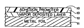
layer are illustrated in Figs. 14. Fig. 1 illustrates a metal foil 10 of the present
invention which comprises metal foil 11, a vapor-deposited layer 12 ovedaying the
metal foil, and an adhesion-promoting layer 13 overlaying the vapor-deposited layer
12.
Fig. 2 illustrates another embodiment of the metal foil 20 of the
invention which comprises the metal foil 21, a vapor-deposited layer 22 overlaying
one side of the metal foil 21, an adhesion-promoting layer 24 overlying the vapor-
deposited layer 22, and a second vapor-deposited layer 23 on the other side of the
metal foil 21. When the metal foil 21 in Fig. 2 is an electrodeposited metal foil
having a shiny side and a matted side, the vapor-deposited layer 22 generally will
overlay the matte side of the metal foil, and the vapor-deposited layer 23 will overlay
the shiny side.
Pig. 3 illustrates yet another embodiment of the metal foil 30 of the
invention wherein the foil has a vapor-deposited layer and an adhesion-promotinglayer on both sides of the foil. In particular, foil 31 is coated on one side with vapor-
deposited layer 32 and on the other side with vapor-deposited layer 33. Adhesion-
promoting layers 34 and 35 overlay and adhere to the vapor-deposited layers 33 and
32, respectively.
Fig. 4 illustrates another metal foil 40 of the invention wherein two
vapor-deposited treatment layers are applied to one side of the metal foil. In
. ~ ., ~:
21~733~
particular, the metal foil 41 is coated on one side with vapor-deposited layer 43, and
then a second vapor-deposited layer 44 is applied over and adheres to vapor-deposited
layer 43. A third layer of vapor-deposited matenal 42 is applied to the other side of
the foil 41. Finally, adhesion-promoting layas 45 and 46 overlay and adhere to the
vapor-deposited treatment layers 44 and 42, respectively.
Another embodiment of the invention (not shown in the Figures)
comprises a copper foil having an electrodeposited-metal coating on both sides of the
foil, a vapor-deposited metal coating on the electrodeposited metal coating on the
matte side, and an adhesion-promoting silane layer overlying and adhered to the
vapor-deposited layer.
The following examples illustrate methods of preparing the metal foils
- . ~
of the invention.
E~amples A-I
A l-ouncelft2 standard profile electrodeposited copper foil is cleaned
lS and microetched by dipping in an aqueous acidic solution containing 20% sulfuric and
1% hydrogen peroxide at 65 C for about 10 seconds. The foil is then rinsed with
deionized water and dried. Chips or a foil of the metal to be deposited are placed on
a tungsten or molybdenum boat in the Edwards apparatus described above, and the
cleaned and microetched copper foil is placed about 5 inches above the evaporation
source inside a Bell jar, and the vacuum is reduced to about 104 millibar or lower
before evaporation proceeds. The metal is evaporated at a fixed current for between
about 0.5 to about 40 minutes. After the vapor deposition process is completed, the
sample is taken out of the apparatus for evaluation.
An aqueous solution containing 0.25 % w of 3-glycidoxypropyltrimeth-
oxysilane and 0.25% w of tetraethoxysilane is prepared, and the foil having the
vapor-deposited layer is coated on both sides by dipping in the solution for 30
seconds. After removing excess solution, the silane-coated foil is then oven-cured for
about I minute at about 90 C. In some of the examples, the microetched foil is
dipped in an aqueous acidic solution containing chromium oxide (CrO3) to provide a
chromium coating either prior to vapor depositing the metal on the foil or subsequent
,
i-
. ~ ,. ...
2~733~
to vapor depositing the metal on the foil. The details of Examples A-I are
summarized in the following Table I.
TABLE I
Standard Profile Raw Foil
Matte Side
V~por Deposited Laver
Chromium Current Time
Example Dip Metal ~ (min)
A No Al 50-65 4-6
B No Zn 35-50 4-10
C No Mn 5~65 4-6
D No In 50-65 6-20
E Yes* In 50-65 6-20
F No Sn 50-65 6-20
G No Ag 35-50 6-15 ~ ;~
H No Co 65-80 0.5-4 ~ -
No Ni 65-80 0.5-4
* Chrome dip after vapor deposition.
Examples~
~. . .- . :...
The general procedure of Examples A-J is repeated except that the raw
foil is a controlled low profile electrodeposited copper foil (1 ouncelft2) having a
substantially uniform randomly oriented grain structure that is essentially columnar
grain-free and twin-boundary free and has an average grain size of up to about 10
-:: ~ ; . :~ .
microns. In addition, as indicated in the following Table II, the vapor-deposited layer
is coated with either 3-glycidoxypropyltrimethoxysilane (Silane-l) or a mixture in `;
water of 0.25% by weight of 3-glycidyloxypropyltrimethoxysilane and 0.25% by
weight of tetraethoxysilane (Mixture-l). The metal is deposited on the matte side of - -
the foil. The details of Examples J-S are summarized in the following Table II.
- ~ .
: .- ~ ' ,:-~.
~. . . . . . .
-` 21~733~
-35-
TABLE II
Çontrolled Low Pro~lle Foil
Matte Side ~ -
Vapor Deposited Laver
S Cumnt Time
- ~ Metal (mA~ (min) Silane Treatment
J Mg 35-50 10-30 Silan~l .
K Mg 35-50 10-30 Mixture-l
L Ti 65-80 4-6 Silane-l .~
M Ti 65-80 4-6 Mixture-l - --
N Cr 65-80 4-6 Silane-1 ~ ~-
O Cr 65-80 4-6 Mixture
P Mn 50-65 4-6 Silane-1 :~
Q Mn 50-65 4-6 Mixture-l
R In 50-65 6-20 Silane-l .
S ln 50-65 6-20 Mixture-1 ~ :`
Examples T-W
The procedure utilized in these examples is similar to the procedure of ~ ;
Examples J-S with the exception that the metal is vapor-deposited on the shiny side
of the copper foil. Details of Examples T-W are summarized in the following Table
III. ~,~,
'` ' :"'
21~73~
-36-
TABLE m
Controlled Low Pro~lle Foil
Shinv Side
Vapor Deposited La~rer -
Cumnt Time
le ~ (mA~ (min) Silane Treatment
T Al 50-65 2-6 Mixtur~l
U Mg 35-50 2-6 Mixture-1
V Zn 35-50 2-6 Mixture-1
W In S~65 2-6 Mixture~
The metal foils of the preænt invention having at least one vapor-
deposited treatment layer overlying and adhered to at least one side of the foil, and
a layer of adhesion-promoting material overlying and adhering to at least one ;
treatment layer are particularly useful for forming laminates by bonding the treated
copper foils to dielectric substrates. Such laminates provide dimensional and
structural stability to the treated copper foils. The combination of the vapor deposited
treatment layer and the adhesion-promoting layer on the foil enhances the bond and
peel strength between the copper foil and the dielectric substrate. One advantage of
the metallic foils of the present invention having the vapor-deposited treatment layer ~ -
and the adhesion-promoting layer is that satisfactory bond and peel strength can be
obtained without having to provide added surface roughening of the foil prior to ~ -
application of the vapor-deposited treatment layer. Even though the metallic foils -
may have a standard profile surface, a low-profile surface or even a very low-profile
surface, desirable peel strengths are obtained as a result of the presence of the vapor-
deposited treatment layer and adhesion-promoting layer. With the foils of the
invention, either the matte side or the shiny side can be effectively bonded to a
dielectric substrate. - ~ `~
Useful dielectric substrates may be prepared by impregnating woven
glass reinforcement materials with partially cured resins, usually epoxy resins (e.g.,
difunctional, tetrafunctional and multifunctional epoxies). Other useful resins include
~:~
21~7 ~3~
-37-
amino type resins produced from the reaction of formaldehyde and urea or
formaldehydeand melamine, polyesters, phenolics, silicones, polyamides, polyimides,
di-allylphthlates, phenylsilanes, polybenzimidazoles, diphenyloxides, polytetrafluoro-
ethylenes, cyanate esters, and the like. These dielectric substrates are sometimes
referred to as prepregs.
In preparing the laminates, it is useful for both the prepreg material and
the copper foil to be provided in the form of long webs of material rolled up in rolls.
~n one embodiment these long webs of foil and prepreg are laminated using a
continuous process. In this process a continuous web of the inventive foil with the
vapor-deposited treatment layer(s) and adhesion-promoting layer(s) adhered thereto
is brought into contact with a continuous web of prepreg material with the adhesive
layer of the foil contacting the prepreg material under laminating conditions to form
a laminate structure. This laminate structure is then cut into rectangular sheets and
the rectangular sheets are then laid-up or assembled in stacks of assemblages.
In one embodiment the long webs of foil and prepreg material are first
cut into rectangular sheets and then subjected to lamination. In this process
rectangular sheets of the inventive foil and rectangular sheets of the prepreg material
are then laid-up or assembled in stacks of assemblages.
Each assemblage may comprise a prepreg sheet with a sheet of foil on
either side thereof, and in each instance, the side (or one of the sides) of the copper
foil sheet with the adhesion-promoting layer adhered thereto is positioned adjacent the
prepreg. The assemblage may be subjected to conventional laminating temperaturesand pressures between the plates of laminating presses to prepare laminates
comprising sandwiches of a sheet of prepreg between sheets of copper foil.
The prepregs may consist of a woven glass reinforcement fabric
impregnated with a partially cured two-stage resin. By application of heat and
pressure, the copper foil is pressed tightly against the prepreg and the temperature to
which the assemblage is subjected activates the resin to cause curing, that is
crosslinking of the resin and thus tight bonding of the foil to the prepreg dielectric
substrate. Generally speaking, the laminating operation will involve pressures in the
-; ~- --- ..... . -. .. . , . . - . . - . . . . . . . .
~ ' - - .
;t: ` ~ .
... ..
2~733~
-38-
range of from about 200 to about 750 psi, more of~en 200 to 500 psi, temperatures
iD the range of from about 70 C to 400 C, more often about 70 C to about 200 C,
and a la ninating cycle of from about a few minutes to about 2 hours. The finished
Iaminate may then be utiliæd to prepare printed circuit boards (PCB).
In one embodiment, the laminate is subjected to a subtractive copper
etching process to form electrically conductive lines or an electrically conductive
pattem as part of a process for making a multilayered circuit board. A second
adhesion-promoting layer is then applied over the etched pattern using the techniques
discussed above and then a second prepreg is adhered to the etched pattern; the
second adhesion-promoting layer being positioned between and adhered to both theetched pattern and the second prepreg. The techniques for making multilayered
circuit boards are well known in the art. Similarly, subtractive etching processes are
well known, an example of which is disclosed in U.S. Patent 5,017,271, which is
incorporated herein by reference.
Laminates obtained by bonding the metal foils of the present invention
to a dielectric substrate are illustrated in Figs. 5 and 6. The laminate 50 of Fig. 5
comprises a metal foil 51 having a vapor-deposited treatment layer 52 overlaying and
adhered to one side of the metal foil 51 and a second vapor-deposited treatment layer
53 overlaying and adhering to the other side of the metal foil 51. An adhesion-
promoting layer 54 overlays and is adhered to the vapor-deposited treatment layer 52
and a dielectric substrate 55 is bonded to the treatment layer 52.
The structure illustrated in Fig. 6 is identical to the structure illustrated
in Fig. 4 with the exception that the foil 60 of Fig. 6 contains an additional adhesion-
promoting layer 65. Thus, Fig. 6 illustrates a metal foil 60 of the invention which
comprises a metallic foil 61 having a vapor-deposited treatment layer 63 on one side
and a vapor-deposited treatment layer 62 on the other side of the metallic foil 61.
Adhesion-promoting layers 64 and 65 overlay and adhere to the vapor-deposited
treatment layers 63 and 62, respectively. A dielectric substrate 66 overlays and is
bo~ded to the adhesion-promoting layer 64.
, : .
: ' .
21~7~3~ ~
-39-
A number of manufacturing methods are available for prepaAng PCBs
from laminates. Additionally, there is a myAad of possible end use applications
including radios, televisions, computers, etc., for the PCB's. These methods and end
uses are known in the art.
S An advantage of the present invention is that the vapor-deposited
treatment layer(s) and the adhesion-promoting layer(s) not only enhance adhesion,
they also provides enhanced oxidation resistance characteristics to the treated foil
particularly when a vapor-deposited layer overlays the shiny side of an electrode-
posited copper foil. This latter characteristic is of particular value due to the fact that
the trend in the industry is for faster and hotter processing practices. Anotheradvantage is that the vapor-deposited treatment layer and the adhesion-promotinglayer provide enhanced acid undercutting resistance to the treated foils.
The improved adhesion exhibited between the copper foils of the
present invention and the polymeric substrates such as multifunctional epoxy prepregs
and difunctional epoxy prepregs is demonstrated by laminating some of the treated
copper foils of Examples described above to a prepreg, and thereafter evaluating the
laminate ~or initial peel strength in pounds/inch using the standard Peel Strength Test
of IPC TM-650. For comparison, each of the unreacted (raw) foils also is laminated
to the prepregs and evaluated. The results of some of these tests are summarized in
the following Table IV.
In Table IV, the examples indicated as control examples correspond to
the referred-to example except that the silane adhesion-promoting layer was not
applied over the vapor-deposited layer prior to lamination. For example, the Control-
A example is a laminate comprising the foil layer, a vapor-deposited aluminum layer
and the indicated prepreg bonded to the aluminum layer. The Example A laminate
comprises the copper foil, an aluminum layer, a silane layer over the aluminum layer
md the prepreg over the silane layer.
.
21~733/~
-40-
TABLE IV
P~d Slm~ T t U~uib
Ini~l P~d St~ndll abrU,)
~OD or Mol~dio~ Diru~ion~
E~mDk Ew~r PrePre Evm~ epree
C~ol A NA' 11.7
i3 ~O.
Con~ol B 53 5.8
C 10.8 NA : :
Conud C 4.6 NA
.~ D 10.5 IO.S
C~ol D 7.3 6.2
1~ ~0.8 1~.8 .
Cootrd ~ 8A 9.6 .. . ~
F 9A NA ~: ~ : '.
Ca~bolP 7.8 NA :: : ::. .
H 11.0 NA ~ 18 ~.:
C~rol H 4A NA :.: ~
'
NA
CllmlJ 0.4 NA -: ::~
K 5.2 NA :: ~ -:
C~d K Q4 NA
L 6.4 NA
C~I L 2.6 NA : :
M 5.8 NA
Conlrol M 2.6 NA
.~: -
T 5A 7.1
Copllol T 5.0 7 3
V 4.8 7.0 . ~ :
Co~uol V ~.2 4.7 . .
W 5.4 53 :::
Conud W 1.8 2.7
Ul~t~
FoD ComD n on~
S_ PoiP ', - :
idc) 2.8
Lmv P~lle Poil '
(m~lle ~idc) 0.4 NA
Low P~lle Foir
( hiny ~ide) 0.2 1.9 ~ ~ .
: ~ ;:
:
' NA = not available. : ~.
45 2 As used in Examples A~
3 As used in Examples J-S.
4 As used in Examples T-W.
2 1 ~ 7 ~
-41~
While the invention has been explained in relation to its preferred
embodiments, it is to be understood that various modifications thereof wiU become
apparent to those skilled in the art upon reading the specification. Therefore, it is to ~ :
be understood that the invention disclosed herein is intended to cover such modifica~
tions as faU within the scope of the appended claims.