Note: Descriptions are shown in the official language in which they were submitted.
W094/09598 2 1 ~ 7 ~ 4 ~ PCT/US93/09827
~ 1
SELECTIVE CALL RECEIVER WIT~ COMPUTER
INTERFACE MESSAGE NOTIFICATION
F;el~ of ~he Tnv~nt; on
This invention relates in general to a Personal Computer
Memory Card Interface Association (PCMCIA) peripheral and more
particularly to a PCMCIA peripheral with selective call
messaging capability.
R~ckaro~n~ of the Tnv~nt; o~
Selective call co~ml~n-cation (paging) systems typically
comprise a radio frequency transmitter/encoder (base station)
that is accessed via a link to the Public Switched Telephone
Network (PSTN) and a radio receiver (e.g., a selective call
receiver or the like) that has at least one unique call
address associated therewith. Operationally, the selective
call receiver receives and decodes information transmitted
from the base station, the information including an address
and possibly a data or voice message. When the selective call
receiver detects its address, it may alert a user and present
message information received.
To implement messaging capability in a paging system, the
address and message information referred to are encoded and
subsequently transmitted using a protocol such as GSC
(Motorola~s Golay Sequential Code) or POCSAG (a code from
Great Britain's Post Office Code Standardisation Advisory
Group). These protocols are adapted to reliably communicate
messages to at least one selective call receiver and are well
known to one of ordinary skill in the art of Paging systems.
A typical selective call message may consist of an address
signal if the message is a tone only message, or an address
signal and a data packet if the message is a data message.
Present selective call receivers operate almost
exclusively in a standalone fashion, that is, received
messages can only be presented by the receiver's display.
Some conventional selective call receivers include a serial
2l~l3~
W O 94/09598 PC~r/US93/09827
data interface for c~mml~nicating a single received message to
an alternate presentation device such as a printer or possibly
an electronic advertising sign. Presently, state of the art
selective call receiver serial communication systems use a
three wire serial interface operating at data rates from 300
to 9600 baud. This serial architecture inherently limits the
data bandwidth (speed and information content) between the
receiver and a data device. Moreover, since the three wire
interface has only transmit data, receive data, and ground
connections, any control signals must be encoded as serial
data symbols, further slowing response time and limiting the
data bandwidth. Lastly, since these interfaces are
proprietary in nature, that is, there is no standard for
signal levels, data rates, or protocols, data interchange
between devices of different manufacturers is all but
impossible because of a lack of convention.
Consequently, what is needed is a standardized
communication interface for state of the art selective call
receiver systems that provides a capability to effectively
communicate received information to a microcomputer or the
like.
~mm~ry of ~he Ir~v~nt; on
Briefly, according to the invention, there is provided a
selective call messaging peripheral capable of receiving at
least one message and communicating it to an electronic
information processing device. The peripheral comprises a
microcontroller including a processor for executing a
microcode program that controls operation of the selective
call messaging peripheral and a receiver that operates to
receive and demodulate an information signal to provide a
recovered information signal including an address signal and
the at least one message. A correlator compares the recovered
address signal with a predetermined address associated with
the selective call messaging peripheral and generates an
address detection when the recovered and predetermined
addresses are substantially equivalent, indicating selection
W094/09598 2 1 ~ 7 3 4 9 PCT/US93/09827
_ 3
of the selective call messaging peripheral. A PCMCIA memory
only interface communicates notification of address detection
to the electronic information processing device, and in
response to a message read command received from the
electronic information processing device, the microcontroller
configures the PCMCIA interface to permit the electronic
information processing device to read the at least one message
from the selective call messaging peripheral.
0 Rr; ef nescri~;on of ~he nr~w;nas
FIG. 1 is a block diagram of a selective call messaging
peripheral having a PCMCIA memory only interface configured
for operation in accordance with the preferred embodiment of
the present invention.
FIG. 2 illustrates an electronic information processing
device having a PCMCIA memory only interface configured for
operation in accordance with the preferred embodiment of the
present invention.
FIG. 3 illustrates a first portion of a PCMCIA memory
only interface table listing signals used for communication
between the selective call messaging peripheral and electronic
information processing device in accordance with the preferred
embodiment of the present invention.
FIG. 4 illustrates a second portion of a PCMCIA memory
only interface table listing signals used for communication
between the selective call messaging peripheral and electronic
information processing device in accordance with the preferred
embodiment of the present invention.
FIG. 5 is a flow diagram illustrating a procedure for the
selective call messaging peripheral to notify the electronic
information processing device of a message receipt in
accordance with the preferred embodiment of the present
invention.
FIG. 6 is a flow diagram illustrating a procedure for the
electronic information processing device to respond when
notified of the message receipt by the selective call
W O 94/09598 PC~r/US93/09827 49 4
messaging peripheral in accordance with the preferred
embodiment of the present invention.
nescri 1~; on of ~ Preferre~l ~smholli ment
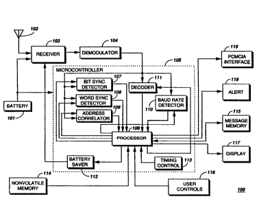
Referring to FIG. 1, a battery 101 powered selective call
messaging peripheral 100 operates to receive an information
signal via an antenna 102. A receiver 103 couples the
received information signal to a conventional demodulator 104
that is capable of recovering analog or digital information.
Received digital information is recovered as a serial bit
stream that is then coupled to a microcontroller 105 for
interpreting and decoding the serial bit stream as address,
control, and data signals. In the preferred embodiment, the
microcontroller 105 may comprise a processor 106, a bit
synchronization detector 107, a word synchronization detector
108, an address correlator 109, a baud rate detector 110, a
data decoder 111, a battery saving control circuit 112, and a
timing control 113, implemented in hardware, software, or a
combination thereof. Examples of commercially available
microcontrollers suitable for implementing the preferred
embodiment of the present invention are Motorola's MC68HC05xx
or M68HCllxx. Complete descriptions of these devices are
available in Motorola's data book set entitled
"Microprocessor, Microcontroller, and Peripheral Data,"
volumes I and II, Series A, ~ 1988 by MOTOROLA, INC.
More specifically, in the microcontroller 105 the serial
bit stream is coupled to the baud rate detector 110 that
determines a receiving data rate associated with the recovered
30 information. When the receiving data rate is determined, the
bit synchronization detector 107 establishes synchronization
between the microcontroller's 105 data decoding components
(106, 109, and 111) and the individual signals (e.g., address,
control, and data signals) in the recovered information. Once
35 bit synchronization is established, the word synchronization
detector 108 searches the serial bit stream for information
indicating the beginning of a batch or frame. When the
microcontroller 105 has established both bit and word
W094/09S98 2 1 4 7 3 4 9 PCT/US93/09827
synchronization, the recovered information may be searched for
a group identification code associated with the selective call
receiver. When a group identification code is found
corresponding to the selective call messaging peripheral, it
5 will search only those code frames associated with the
receiver's group for pages intended for the selective call
messaging peripheral. During the period between like frames,
the microcontroller 105 will preferably activate the battery
saver 112 to "shut-down" the receiver 103 and demodulator 104,
thereby conserving power and extending battery life. The
interval between like frames is known in the art as a "sleep"
period. Preferably, the system protocol operates such that
pages targeted for a specific group identifier, and pages
intended for a particular selective call messaging peripheral,
are sent only during the transmission of that receiver's
designated paging group, therefore, no pages are missed during
the sleep period. A receiver that operates in this fashion is
said to be in a "battery saving" mode.
In determining the selection of the particular selective
call messaging peripheral, a correlation is performed between
a predetermined address associated with the selective call
receiver and a received address. To accomplish this, the
address correlator 109, which comprises a signal processor,
performs a comparison between the address signal recovered
from the received information signal and a predetermined
address associated with the selective call messaging
peripheral, generating a detection indicating selection of the
selective call messaging peripheral when the recovered address
is substantially equivalent to the predetermined address. The
predetermined address or addresses associated with the
selective call messaging peripheral are preferably stored in
the non-volatile memory 114 or code plug. Optionally, the
non-volatile memory 114 may reside inside a support integrated
circuit (not shown) or in the microcontroller 105. The non-
volatile memory 114 typically has a plurality of registers forstoring a plurality of configuration words that characterize
the operation of the selective call messaging peripheral.
When a detection is generated, the microcontroller 105 may
W O 94/09598 ~ 3 ~ PC~r/US93/09827
generate an alert responsive to a selected alerting mode,
e.g., a tone alert would be generated when a tone-only mode is
selected. Alternatively, in response to a valid data address
correlation and a corresponding detection, the decoder 111
operates to decode at least one selective call message from
the received information signal and couples message
information to the message memory 115.
In accordance with the recovered information, the
programmed operating parameters stored in the non-volatile
memory 114, and settings associated with the user controls
116, the selective call messaging peripheral may present at
least a portion of the message information, such as by a
display 117. Alternatively, the user may be alerted that a
message has been received by an alert transducer 118 that
generates an audible, visual, or tactile alert. The user may
view received message information on the display 117 by
manually activating an appropriate user control 116 such as a
message read control 116.
The microcontroller 105 may also include items such as a
conventional signal multiplexer, a voltage regulator and
control mechanism, a current regulator and control mechanism,
environmental sensing circuitry such as for light or
temperature conditions, audio power amplifier circuitry,
control interface circuitry, and display illumination
circuitry. These elements are arranged in a known manner to
configure the selective call messaging peripheral as requested
by a customer.
In the preferred embodiment, upon receipt or storage of a
selective call message, the microcontroller 105 may
communicate the received message to an electronic information
processing device (e.g.~ a host microcomputer or the like as
illustrated in FIG. 2) via a PCMCIA interface 119. When
coupled to the electronic information processing device 200,
the selective call messaging peripheral 100 may operate to
automatically deliver received messages in real time, or
transfer stored messages to the electronic information
processing device for storage, presentation, archival, or the
like. Alternatively, a user may via a program executing on
2Iq734g
W O 94/09598 PC~r/US93/09827
. _
the electronic information processing device, download any
messages previously received and stored by the selective call
messaging peripheral 100 while in the standalone operating
mode (separated from the electronic information processing
- 5 device). In this way, the selective call messaging peripheral
100 gives a paging subscriber the option of operating as a
conventional standalone paging receiver, that is, receiving,
storing and displaying messages. It is for this reason that
the selective call messaging peripheral 100 includes a message
read control for recalling the at least one selective call
message from the at least one electronic memory 115 for
presentation. This allows a user to present the at least one
selective call message recalled from the at least one
electronic memory 115 on the display 117 in response to
activating the message read control 116.
As can be appreciated by one of ordinary skill in the
art, this invention can be realized in a number of embodiments
of which the disclosed embodiment is only one of many
equivalent alternatives.
Referring to FIG. 2, the illustration shows a electronic
information processing device 200 having a PCMCIA interface
configured for operation in accordance with the preferred
embodiment of the present invention. As illustrated, the
electronic information processing device 200 comprises a
25 system timing clock 201, central processing unit 202, random
access memory (RAM) 203, read only memory (ROM) 204, mass
storage (e.g.t a disk drive or the like) 205, display driver
206, general I/O interfaces 207, and a PCMCIA memory only
interface 208. In the preferred embodiment, the electronic
information processing device's PCMCIA memory only interface
208 couples to the selective call messaging peripheral's 100
PCMCIA interface 119. After coupling, messages received by
the selective call messaging peripheral 100 may be
communicated to the electronic information processing device
200 via the PCMCIA memory only interface 208 and directed to
the electronic information processing device's RAM 203, mass
storage 205, display driver 206 for presentation on an
external display (not shown)~ or possibly to one of the
W094/09598 ~349 PCT/US93/09827
general I/O interfaces 207 for routing to a printer or the
like.
The system formed by coupling the elements depicted in
FIG. 1 and FIG. 2 via a PCMCIA memory only interface realizes
many advantages over prior art selective call messaging
systems. Since the PCMCIA interface is a standard, the
selective call messaging peripheral 100 need not be customized
for operation with dissimilar host computers supporting the
PCMCIA standard. This eliminates the problems associated with
proprietary interface standards such as no standard for signal
levels, data rates, or protocols, making data interchange
between devices of different manufacturers is all but
impossible. Another advantage of the PCMCIA interface
implemented in the selective call messaging peripheral 100
over the conventional three wire serial communication systems
is data throughput. Since the PCMCIA interface can
accommodate 16 bit parallel data transfers, and includes DMA
(direct memory access) capability, there is a significant
increase in data bandwidth as opposed to a 9600 baud, 8 bit,
asynchronous serial data link. Moreover, the PCMCIA interface
implements dedicated control signals, and may even provide
power for the selective call messaging peripheral 100.
Referring to FIG. 3 and FIG. 4, the illustrations show a
first and a second portion of a PCMCIA memory only interface
table listing signals used for communication between the
PCMCIA selective call messaging peripheral and electronic
information processing device in accordance with the preferred
embodiment of the present invention.
The tables illustrated in FIG. 3 and FIG. 4 detail the
PCMCIA memory only interface pinout and signal definitions.
The PCMCIA memory only interface standard includes provisions
for reading 16-bit data on the low-order 8 bit data bits
(useful in conventional 8-bit host systems) and for the
interpretation of status information returned by a PCMCIA
peripheral card. The principal aspects of the PCMCIA card
interface are byte addressability, random access to bytes of
data, and the existence of a separate "register" attribute
memory space selected by a REG signal. This allows an
W O 94/09598 2 1 ~ 7 3 4 9 PC~r/US93/09827
-
electronic information processing device to obtain highly
detailed peripheral card information such as its manufacturer
or a chip-type. The PCMCIA standard also allows access to
control registers in configurable types of cards.
5The standard PCMCIA interface depicted has a 64-Mbyte
addressing capability and numerous hardware provisions to
support the various memory technologies, including ROM,
OTPROM, W -EPROM, FLASH, SRAM and PSRAM. I/O-card support is
provided in the PCMCIA I/O interface (not shown) by Interrupt,
16-bit cycle, IOread/IOwrite, INput ACK, Reset, Wait, Status
Change, Enable and Power signals, some of which are
dynamically redefined to these uses once an I/O card is
recognized by the host.
All signals in the PCMCIA interface are grouped under
four classifications: I (Input), O (Output), I/O
(Bidirectional), and R (Reserved). Input signals are those
driven by the electronic information processing device and
output signals are those driven by the peripheral card.
The Memory-Only Interface supports memory cards, but does
not contain signals which support I/O Cards. The preferred
embodiment of the present invention implements the Memory-Only
Interface as defined by PCMCIA. The signals +RDY/-BSY, WP,
BVDl and BVD2 are present on the Memory-Only Interface but are
replaced by other signals when the I/O Interface is selected.
The Memory-Only Interface is selected by default in both the
socket and the card whenever a card is inserted into a socket,
and immediately following the application of Vcc (power) or
the RESET signal to a card. After a card's Card Information
Structure (CIS) has been interpreted, the card and the socket
may be configured, if appropriate, to use the I/O Interface.
PCMCIA peripheral cards may be configured by the
electronic information processing device to change the way
that their address space is accessed. Before configuring a
card, the electronic information processing device must
~ 3mine the card's CIS to determine the address space and
other requirements of the possible card configurations. The
electronic information processing device uses this information
to select the best configuration from those available in the
W094/09598 2~4~ 3 4~ PCT/US93/09827
card, as determined by the electronic information processing
device's hardware and software capabilities, as well as the
requirements of other cards installed concurrently. Both the
electronic information processing device and peripheral card
may play a role in determining when the latter is selected.
The card includes information in the CIS which tells the host
the address decodings the card may be configured to perform.
The host then programs the card to perform a particular
decoding using the card's Configuration Registers.
The PCMCIA memory only interface signals illustrated in
FIG. 3 and FIG. 4 are detailed in the following text along
with their functions. Signals A0 through A25 are address-bus-
input lines which enable direct address of up to 64 megabytes
of memory on the card. Signals D0 through D15 constitute the
bidirectional data bus. The -CEl signal enables even-
numbered-address bytes and -CE2 enables odd-numbered-address
bytes. A multiplexing scheme based on A0, -CEl and -CE2
allows 8-bit microcomputer hosts to access all data on D0
through D7 if needed. The -OE line is used to gate Memory
Read data from the memory card. The -WE/-PGM input signal is
used for strobing Memory Write data into a PCMCIA memory card.
This line is also used for memory cards employing programmable
memory technologies. A Ready/Busy function is provided by the
+RDY/-BSY signals when the peripheral card and the
microcomputer host socket are configured for the Memory-Only
Interface. The -CD1 and -CD2 signals provide for proper
detection of memory-card insertion. Their signal pins are
located at opposite ends of the connector to ensure a valid
detection (i.e., ensuring both sides of the card are firmly
inserted). In a conventional implementation of the PCMCIA
memory only interface, the -CD1 and -CD2 signals are connected
to ground internally on the memory card and will be forced low
whenever a card is placed in a host socket. The preferred
embodiment of the present invention implements grounding of
the -CD1 and -CD2 signals using electronic means such as an
open collector transistor, an integrated circuit driver, or
the like. This implementation allows the selective call
messaging peripheral 100 to request service from the
2~7~
W094/09598 PCT/US93/09827
, _
11
electronic information processing device 200 by toggling the
state of the -CDl and -CD2 lines, thereby "tricking" the
- electronic information processing device's PCMCIA interface
driver into thinking that the selective call messaging
peripheral was temporarily removed (disconnected) from the
electronic information processing device 200. Since the
PCMCIA interface driver as defined in the PCMCIA specification
must interrogate a PCMCIA card when inserted (e.g., when
ground is detected on the -CDl and -CD2 lines), this procedure
essentially allows a PCMCIA memory only interface card to
request service from a host device in a fashion similar to an
interrupt as defined in the PCMCIA I/O interface standard.
The WP output signal is used to reflect the status of the
card's Write Protect switch. The -REG signal is kept inactive
for all Common Memory access. The signals BVDl and BVD2 are
generated by the memory card as an indication of the condition
of its battery. The VPPl and VPP2 signals supply programming
voltages for programmable-memory operation, or additional
supply voltages for Peripheral Cards. The Vcc and GND input
pins are located at symmetrical positions on the memory card
to provide safety in the case of an inverted-card insertion.
The Refresh signal is intended for pseudostatic SRAMS (PSRAM).
Several pins have been identified as Reserved for Future Use
(RFU). The +RESET signal clears the Card Configuration Option
Register thus placing a card in an unconfigured (Memory-Only
Interface) state. It also signals the beginning of any
additional card initialization. The -WAIT signal is asserted
by a card to delay completion of the memory-access cycle in
progress.
As can be seen from the preceding discussion, using a
PCMCIA memory only interface in conjunction with a selective
call receiver for message delivery to a electronic information
processing device 200 yields distinct advantages in expanding
the functionality of the selective call messaging peripheral
100. The interface is capable of adaptive configuration to
both 8 and 16 bit wide bus architectures, as well as
supporting other features such as low battery detection. A
conventional serial interface cannot implement the wide array
W094/09598 ~3~ PCT/US93/09827
12
of features available in the PCMCIA interface standard. Even
if some of the simpler features were implemented using a
conventional serial interface, the implementation would
require added complexity in terms of device and comm~nd
handlers in both the host and peripheral systems and would not
be able to achieve functional equivalence to a PCMCIA
implementation.
Referring to FIG. 5, the flow diagram illustrates a
procedure for the selective call messaging peripheral to
notify the electronic information processing device of a
message receipt in accordance with the preferred embodiment of
the present invention. When a selective call message is
received by the selective call messaging peripheral 501, an
unread message is stored and step 502 passes control to step
503. Step 503 test for notification of the electronic
information processing device. If the device has not been
notified, the selective call messaging peripheral communicates
notification of the address detection to the electronic
information processing device 504. Notification can be
effected in two ways. In a first embodiment, the electronic
information processing device is notified by simulating
disengagement of the PCMCIA memory only interface between the
selective call messaging peripheral and the electronic
information processing device, the simulated disengagement
causing the electronic information processing device to issue
the message read cnmm~nd to the selective call messaging
peripheral. The simulation is accomplished by changing an
impedance present at a connection corresponding with at least
one card detect signal (e.g.l the -CDl and -CD2 lines) on the
selective call messaging peripheral's PCMCIA memory only
interface from a first electrical state approximating a zero
impedance reference with respect to a relative ground
reference potential for the PCMCIA memory only interface to a
second electrical state approximating an infinite impedance
and then returning the impedance to the first electrical
state. In a second embodiment, the electronic information
processing device is notified by executing a sequence that
asserts a PCMCIA busy signal in the selective call messaging
VVO 94/09598 ~I ~ 7 3~ 9 PC~r/US93/09827
" ,
13
peripheral's PCMCIA memory only interface, then releases the
PCMCIA busy signal and asserts a PCMCIA ready signal in the
- selective call messaging peripheral's PCMCIA memory only
interface, the sequence causing the electronic information
5 processing device to issue the message read command to the
selective call messaging peripheral. In each embodiment, the
final result is that the electronic information processing
device is notified of an unread message received and the
message is made available for transfer to and processing by
10 the electronic information processing device. When message
processing is complete, control is returned to the selective
call messaging peripheral's main control program 505.
Referring to FIG. 6, the flow diagram illustrates a
procedure for the electronic information processing device to
15 respond when notified of the message receipt by the selective
call messaging peripheral in accordance with the preferred
embodiment of the present invention. The procedure starts 601
and checks for either the card detect signal being false
(indicating the card has been removed) or the PCMCIA memory
20 only interface busy signal being asserted 602. If either of
these conditions are affirmed, step 603 determines if a
"special" card (e.g.~ a selective call messaging peripheral
card or the like) was present in the PCMCIA memory only
interface slot. If the special card was present, a flag
25 indicating its presence is set 604, a time-out timer started
605, and control is returned to the electronic information
processing device's main control program 606. After
determining that a selective call messaging peripheral card
has been removed and reinserted (or the PCMCIA interface
30 signals CDl, CD2, indicate such an event has occurred) 602,
603 and that a special card was present in the PCMCIA memory
only interface slot 609, and that the flag indicating a card
was present is set 609, the flag is reset 610 and the time-out
time checked to prevent a false indication of unread messages.
35 If the timer had not expired, the electronic information
processing device issues a message read command to the
selective call messaging peripheral card via the memory only
PCMCIA interface 612. If there are unread messages 613, the
PCT/US93/098?7
14
electronic information processing device addresses the
selective call messaging peripheral card and may read the
unread messages into its RAM, store them in its mass storage,
or present them on its display. When message processing is
complete, control is returned to the electronic information
processing device's main control program 606.
What is claimed is: