Note: Descriptions are shown in the official language in which they were submitted.
WO 94/12950 ~ ~ ~ ~ 8 ~ PCT/US93111314
-1-
GLUCOSE TEST DATA ACQUISITION AND MANAGEMENT &YSTEM
Tec~~'cal Field and Industrial Applicabilit
This invention relates to methods and apparatus
for adapting instruments to a common protocol for
communication with, for example, a data gathering and
processing system. The invention is disclosed in the
context of glucose monitoring instruments, but it is
believed to be useful in other applications as well.
Background Art
Test strip-reading, glucose monitoring
instruments of various types are in common use today.
There are, for example, the ACCUTREND, ACCU-CHEK II, ACCU-
CHEK III and ACCU-CHEK EASY instruments, all available from
Boehringer Mannheim Corporation, 9115 Hague Road,
Indianapolis, Indiana 46250-0528. There are also the
instruments described in U.S. Patents: 4,685,059;
4,168,469; 4,747,060; 4,751,648; 4,791,570; 4,882,704;
4,882,705; 4,902,948; 3,907,503; 3,980,437; 4,160,646;
4,509,859; 4,676,653; 4,871,258; 4,934,817; 5,037,614;
5,039,615; 5,053,199; 5,059,394; 5,055,261; 5,047,351;
4,791,461; 4,309,112; 3,989,383; 3,881,992; and, 4,093,849;
European Published Patent Application EP 387,630 A2;
Japanese Published Patent Applications: 63-269,046 and 63-
61,147; German Published Patent Application 2,319,465;
Diabetes, Vol. 33, Supplement 1, issued May 1984, D.
Michaels et al., "A MEMORY-GLUCOSE REFLECTANCE METER FOR
AUTOMATIC DATA RECORDING," entry 498, pg. 103A; Diabetes,
Vol. 33, Supplement 1, issued May 1984, J. Silverstein et
al., "COMPARISON OF SYSTEMS FOR BLOOD GLUCOSE MONITORING
WITH A METER: ACLU-CHEK AND GLUCOMETER," entry 502 pg.
131A; Diabetes, Vol. 33, Supplement 1, issued May 1984, D.
Hiennen et al., "ASSESSMENT OF ACCURACY OF il GLUCOSE
MACHINES FOR HOME USE," entry 503 pg. 131A; and Diabetes,
WO 94112950 PC"f/US93/11314
~~~r4~~
-2-
Vol. 33, Supplement 1, issued May 1984, V.G. Kuykendall et
al., "INFORMATION MANAGEMENT FOR GLUCOMETER REFLECTANCE
PHOTOMETER WITH MEMORY," entry 507, pg. 132A.
U.S. Patent 5,153,416, discloses a portable,
microcomputer-controlled device including a bar code reader
for reading a patient's I.D. bracelet bar code and printing
out labels for specimen bottles including the patient's
I.D., the tests) to be performed on the specimen, the
time, the date, and the like. U.S. Patents 4,118,687 and
4,121,574 also disclose bar code readers for use in this
environment. U.S. Patent 3,872,448 discloses a hospital
data management system. U.S. Patent 4,715,385 discloses a
patient monitoring system with a detachable monitor signal
processing section which can be plugged into mobile or
stationary displays to drive them. U.S. Patents:
4,890,832; 4,523,297; arid, 4,853,682 all diSClOSe Systems
which have a common component, such as a base, and several
special components adaptable to the base. U.S. Patent
4,571,702 discloses a zero power remote program storage and
retrieval system. U.S. Patent 5,110,226 discloses a system
which communicates with an external computer. U.S. Patents
4,731,726 and 5,019,974 disclose diabetes management
systems. U.S. Patents: 4,519,398; 4,546,436; and
4,779,199 all disclose patient monitors.
Many health care providers, such as hospitals,
have substantial numbers of glucose measuring instruments
of various different types with which numbers of glucose
measurements are made on numbers of patients each day.
Typically, the instruments have been acquired by the health
care provider at different times; and so different types of
instruments are used routinely. It is generally desirable
to keep patient glucose readings and related data over
extended periods of time, to be able to perform certain
calculations, such as statistical studies, on that data,
and to print hard copies of the raw data, calculation
78807-9
CA 02147484 2001-04-04
3
results and so on. Frequently, the glucose measuring
instruments themselves are not equipped to connect to, for
example, printers to provide hard copies. Similarly, the
glucose measuring instruments themselves may not have the
capacities to store large numbers of patient glucose readings
or to perform the desired calculations, even on the small
numbers of readings they are equipped to store.
SUMMARY OF THE INVENTION
An instrument according to the invention has the
capability to: 1) interface with a printer for printing
quality control reports, patient records and the like; (2)
store larger numbers of patient glucose readings and related
data than glucose measuring instruments typically are capable
of storing; (3) perform various calculations on the data; (4)
interface both to a number of different types of glucose
measuring instruments and to a "notebook"-type computer which
is capable of even greater data storage and calculation
capability than the instrument of the invention itself; and (5)
provide a system lockout if quality control results of the unit
are out of range.
According to one aspect of the invention, there is
provided a system for adapting one of a number of different
types of instruments to a common protocol, each instrument
having a first serial input-output (I/O) port, first means for
controlling the serial I/O port, and second means for
furnishing operating power to the instrument, the system
including a different type of housing for each different type
of instrument, each different type of housing including means
defining openings through which selected controls and displays
of a respective one of the instruments are accessible, each
different type of housing including third means for coupling to
7 8 8 O 7 - 9 CA 02147484 2001-04-04
4
a respective type of instrument's first serial I/O port, fourth
means for coupling to a respective type of instrument's second
means, and a data processing module including a first multiple
conductor connector, each type of housing including a
complementary second multiple conductor connector for
connecting to the first multiple conductor connector when a
respective housing is mated to the data processing module.
Illustratively, according to this aspect of the
invention, the second means comprises a battery enclosure
having first and second battery terminals. The fourth means
comprises a battery emulator having third and fourth terminals
for engagement by the first and second battery terminals,
respectively, when an instrument of the respective type is
housed in a housing of the respective type. Fifth means couple
the third and fourth terminals across a source of operating
power for the respective instrument.
WO 94/12950 PCT/US93I113I4
21~'~~~~
-5-
Illustratively according to this aspect of the
invention, the data processing module further comprises
first slide members. Each type of housing further
' comprises complementary second slide members for engagement
with the first slide members when a respective housing
engages the data processing module.
Illustratively according to this aspect of the
invention, the data processing module further comprises a
data processing module power supply. Ninth means couple
the power supply across a pair of conductors of the first
multiple conductor connector. Mating of a respective
housing to the data processing module connects that
respective housing, its respective first microprocessor,
and a respective instrument housed in that respective
housing to the data processing module power supply.
Illustratively according to this aspect of the
invention, the data processing module further comprises
tenth means for coupling the data processing module to an.
external power supply, and eleventh means for coupling the
external power supply across a pair of conductors ~f the
first multiple conductor connector. Mating of a respective
housing to the data processing module connects that
respective housing, its respective first microprocessor,
and a respective instrument housed in that respective
housing to the external power supply.
Additionally illustratively according to this
aspect of the invention, the data processing module further
comprises a second microprocessor having a second
microprocessor I/O. Twelfth means couple respective
conductors of the first multiple conductor connector across
' a first group of pins of the second microprocessor's I/O.
Thirteenth means couple a second group of pins of the
second microprocessor I/O to respective terminals of the
secona serial I/O port.
,7 8 8 O 7 - 9 CA 02147484 2001-04-04
6
Further illustratively according to this aspect of
the invention, the thirteenth means comprises an RS232-to-
transistor-transistor logic (TTL)/TTL-to-RS232 interface.
Additionally illustratively according to this aspect
of the invention, the thirteenth means comprises an optical
isolator. A receive data terminal of the second serial I/O
port is coupled to a light source portion of the optical
isolator. Fourteenth means couple a light activated switch
portion of the optical isolator to an RS232-to-TTL received
data output terminal of the RS232-to-TTL/TTL-to-RS232
interface.
According to this aspect of the invention, the
fourteenth means comprises an interrupt pin of the second
microprocessor I/O.
Additionally according to this aspect of the
invention, fifteenth means switches power to the RS232-to-
TTL/TTL-to-RS232 interface. The fifteenth means is coupled to
the second means, to an operating power supply terminal of the
RS232-to-TTL/TTL-to-RS232 interface, and to the interrupt pin
of the second microprocessor I/O. Receipt of data on the
receive data terminal of the second serial I/O port causes
power to be supplied from the second means to the operating
power supply terminal of the RS232-to-TTL/TTL-to-RS232
interface to activate the RS232-to-TTL/TTL-to-RS232 interface
and to activate a switch in the RS232-to-TTL output terminal of
the RS232-to-TTL/TTL-to-RS232 interface.
According to another aspect the invention provides a
system for adapting one of a number of different types of
instruments to a common protocol, each instrument having a
first serial input-output (I/O) port, first means for
controlling the serial I/O port, and second means for
,7 8 8 O ,7 - 9 CA 02147484 2001-04-04
7
furnishing operating power to the instrument, the system
including a different type of housing for each different type
of instrument, each different type of housing including means
defining openings through which selected controls and displays
of a respective one of the instruments are accessible, each
different type of housing including third means for coupling to
a respective type of instrument's first serial I/O port and
fourth means for coupling to a respective type of instrument's
second means, the third means comprising a first
microprocessor, sixth means for conditioning the signals at the
first I/O port, seventh means for coupling the first I/O port
to the sixth means, and eighth means for coupling the sixth
means to the first microprocessor.
According to another aspect the invention provides a
system for adapting one of a number of different types of
instruments to a common protocol, each instrument having a
first serial input-output (I/O) port, first means for
controlling the serial I/O port, and second means for
furnishing operating power to the instrument, the system
including a different type of housing for each different type
of instrument, each different type of housing including means
defining openings through which selected controls and displays
of a respective one of the instruments are accessible, each
different type of housing including third means for coupling to
a respective type of instrument's first serial I/O port and
fourth means for coupling to a respective type of instrument's
second means, the openings including an opening for a
prompt/test results display for the respective instrument, and
an opening for insertion of unreacted/reacted test strips for
the respective instrument.
7 8 8 O 7 - 9 CA 02147484 2001-04-04
7a
According to yet another aspect the invention
provides a system for adapting one of a number of different
types of instruments to a common protocol, each different type
of instrument being for determining the concentration of a
medically significant component of a body fluid, each
instrument having a first serial input-output (I/O) port, first
means for controlling the serial I/O port, and second means for
furnishing operating power to the instrument, the system
including a different type of housing for each different type
of instrument, each different type of housing including means
defining openings through which selected controls and displays
of a respective one of the instruments are accessible, each
different type of housing including third means for coupling to
a respective type of instrument's first serial I/O port and
fourth means for coupling to a respective type of instrument's
second means, a data processing module including a first
multiple conductor connector, each type of housing including a
complementary second multiple conductor connector for
connecting to the first multiple conductor connector when a
respective housing is mated to the data processing module.
According to still another aspect the invention
provides a system for adapting one of a number of different
types of instruments to a common protocol, each different type
of instrument being for determining the concentration of a
medically significant component of a body fluid, each
instrument having a first serial input-output (I/O) port, first
means for controlling the serial I/O port, and second means for
furnishing operating power to the instrument, the system
including a different type of housing for each different type
of instrument, each different type of housing including means
defining openings through which selected controls and displays
of a respective one of the instruments are accessible, each
different type of housing including third means for coupling to
7 8 8 O .7 - 9 CA 02147484 2001-04-04
7b
a respective type of instrument's first serial I/O port and
fourth means for coupling to a respective type of instrument's
second means, the third means comprising a first
microprocessor, sixth means for conditioning the signals at the
first I/O port, seventh means for coupling the first I/O port
to the sixth means, and eighth means for coupling the sixth
means to the first microprocessor.
BRIEF DESCRIPTION OF THE DRAWINGS
The invention may best be understood by referring to
the following description and accompanying drawings which
illustrate the invention. In the drawings:
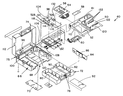
Fig. 1 illustrates an exploded perspective view of an
instrument constructed according to the invention;
Fig. 2 illustrates a perspective view of the
instrument of Fig. 1 assembled, with a housing containing one
of the glucose measuring instruments with which the instrument
of Fig. 1 is capable of interfacing removed from it;
224 ~~~~ , ,
5727- ,522 PCT/US ~ 3 ~ 1 1 4
03 Recd ~'t~/~~~ ~ ? ,!~.,'~~ ~9~~
_8_
Fig. 3 illustrates the glucose measuring
instrument of Fig. 2, and its housing in exploded
perspective;
Fig. 4 illustrates in partly block and partly
schematic form a circuit contained within the housing of
Fig. 3;
Fig. 5 illustrates another glucose measuring
instrument with which the instrument of Fig. 1 is capable
of interfacing, and the housing for that glucose measuring
instrument in exploded perspective;
Fig. 5a illustrates an enlarged fragmentary
sectional view of a detail of Fig. 5, taken generally along
section lines 5a-5a of Fig. 5;
Fig. 6 illustrates in partly block and partly
schematic form a circuit contained within the housing of
Fig. 5;
Fig. 7 illustrates another glucose measuring
instrument with which the instrument of Fig. 1 is capable
of interfacing, and the housing for that glucose measuring
instrument in exploded perspective;
Fig. 8 illustrates in partly block and partly
schematic form a circuit contained within the housing of
Fig. 7;
Fig. 9 illustrates another glucose measuring
instrument with which the instrument of Fig. 1 is capable
of interfacing, and the housing for that glucose measuring
instrument in exploded perspective;
Fig. 10 illustrates in partly block and partly
schematic form a circuit contained within the housing of
Fig. 9; and,
Figs. lia-j illustrate in partly block and partly
schematic form circuits contained within the instrument of
Fig. 1.
ntacmnrn cuct~
WO 94/12950 ~ PCT/US93/113i4
-9-
Modes for Carrying Out the Invention
Fig. 1 illustrates an exploded perspective view
of a remote glucose test station (GTS) 40 for incorporating
a selected one of a number of different glucose meters,
illustratively, the Boehringer Mannheim Corporation
ACCU-CHEK II 42, ACLU-CHEK III 44, ACCU-CHEK EASY 46, and
ACCUTREND 48 meters. The GTS 40 includes provisions for
storing data, such as date, time, glucose reading and a
patient identifier, related to a number of glucose readings
from each of a number of patients taken from the meter 42,
44, 46 or 48 incorporated into it, for providing this
information in (a) suitable (formats) t~ a printer (not
shown) coupled to a printer port on the GTS 40, and/or for
supplying this information in such formats) to a hospital
data management (HDM) system (not shown) through a port
provided for such communication on GTS 40. A suitable
printer is one which is supported by the IBM/Epson
standard. A suitable HDM system would be, for example,
Digital Equipment Corporation's DEC320P (Model PCP11)
.notebook computer. GTS 40 also includes a bar code reader
port for coupling a bar code reader (not shown), such as,
for example, a Welch Allyn Model 6180/A-25999247 bar code
reader, to GTS 40.
GTS 40 includes a top 50 with a relief 53 for a
keypad 54. Keypad 54 is provided with an opening 56
covered by a lens 58 through which a display 60 is visible.
A well 61 is provided in top 50 for, for example, a vial of
unreacted blood glucose measurement strips. A midplate 62
on which are mounted the main GTS printed circuit board
(PCB) 64 and other GTS hardware is captured between top 50
and GTS base 66 by appropriate threaded fasteners which
extend upward through base 66 and midplate 62 and into top
50. PCB 64 is mounted to midplate 62 by appropriate
threaded fasteners. Base 66 is provided with a central
battery well 68 which houses, for example, six "C" cells
WO 94/12950 PCTIUS93/11314
2~4'~4~~
-10-
(not shown) which are inserted into the well 68 from the
underside of base 66. A battery well cover 70 snaps into
closing orientation to close well 68.
A storage drawer 72 is slidable between base 66
and midplate 62. A cover 74 is hinged 75 at the rear of
base 66. Drawer 72 is prevented from inadvertently sliding
out of base 66 and cover 74 is prevented from inadvertently
opening when cover 74 is closed by engagement of a tab 76
on the front of drawer 72 in an opening 78 on the front of
cover 74. Drawer 72 is provided with left and right
storage compartments 80, 82, respectively, each of which
can accept longitudinal 84 or transverse 86 dividers for
dividing the compartment 80, 82 into smaller compartments.
These compartments are convenient for holding bandages,
antiseptic swabs, and other equipment necessary for the
taking of, for example, blood samples from the pricked
fingers of diabetes sufferers for measurement by a glucose
meter 42, 44, 46 or 48 incorporated into GTS 40 in a manner
to be described.
The central area 90 of drawer 72 is provided with
a "comments code" chart 92 which desirably contains
comments to patient record data encoded into bar code. In
operation, a health care provider may wish to add comments
to patient record data after a reading is taken for storage
in the GTS 40. The health care provider can pick the
correct code from chart 92, pass the bar code reader over
the bar code accompanying that comment and have that
comment entered with the patient record data. A connector
96 and associated insulated conductors supply power from
the battery well 68 to the battery power socket 98 on PCB
64. Alternatively, power can be supplied from an external
low voltage DC source through a socket 100 accessible
through the rear of base 66 and associated insulated
conductors to a connector 102 and external DC supply socket
104 provided on PCB 64. A bar code reader port 106 is
WO 94/12950 PCT/US93/11314
-11-
accessible with cover 74 closed or open by virtue of
notches 110, 112 in the lower left-hand side edges of top
50 and cover 74, respectively. Appropriate insulated
conductors and connectors extend from port 106 and a serial
I/O (RS232) port 108 to sockets 114, 116 provided on PCB 64
for entry of bar code and serial I/O, respectively. A
printer port 118 mounted on PCB 64 is accessible with cover
74 open by virtue of notch 110.
The front right-hand side area 120 of top 50 is
generally flat and provided with a pair of parallel,
somewhat inverted L-shaped transverse section slides 122.
As best illustrated in Fig. 2, these slides 122 permit one
of four housings 124 (Figs. 2-3), 126 (Fig. 5), 128
(Fig. 7), 130 (Fig. 9), each provided with a complementary
pair of parallel slides 125, 127, 129, 131, respectively,
to be slid from the right onto slides 122 until the
respective housing 124, 126, 128, 130 occupies area 120.
An appropriate threaded fastener can then be inserted
through the base 66 into an. opening (not shown) provided
therefor in the bottom of housing 124, 126, 128, 130 to
lock housing 124, 126, 128, 130 onto GTS 40. A nine-pin
connector 132 provided on PCB 64 engages a complementary
connector socket 134, 234, 334, 434 associated with the
respective housing 124, 126, 128, 130 when the housing 124,
126, 128, 130 is slid fully into position on GTS 40. All
of the required electrical connections between the meter in
housing 124, 126, 128 or 130 and the remaining electronics
of GTS 40 are made by this act.
Housing 124 and its contents are better
illustrated in Fig. 3, an exploded perspective view of
these components. The illustrated meter 42 is a Boehringer
Mannheim Corporation ACCLT-CHEK II blood glucose meter.
Housing 124 includes a housing bottom 138 provided with the
previously mentioned slides 125 and a back 140 which
extends generally perpendicularly to bottom 138. A wall
WO 94/12950 PCT/US93111314
-12-
142 extends forward from back 140 along the left edge of
bottom 138 to mount the connector socket 134. An insulated
multiple conductor cable 144 extends from socket 134 to
complementary connectors 146, 148 provided on a printed
wiring board (PWB) 150 on which is mounted an adaptive
communications processor (ACP) 152, illustrated in partly
block and partly schematic circuit form in Fig. 4. The PWB
150 is mounted to bottom 138 at the rear thereof, adjacent
back 140, by appropriate threaded fasteners. The meter 42
is connected electrically to the circuitry on PWB 150 by a
complementary connector 154 and socket 156. Connector 154
is mounted on PWB 150. Socket 156 is provided on one end
of an insulated multiple conductor cable 158, the
conductors of which are split into two groups intermediate
the ends of cable 158 and provided with separate adaptor
sockets 160 and 162 to supply power to the meter 42 and a
connection to the meter 42's serial I/O port, respectively.
The housing 124 top is divided into a rear
portion 164 and a front portion 166 which are hinged 168
together. The rear top portion 164 is secured to the
bottom 138 by a suitable threaded fastener, which
simultaneously captures PWB 150 between rear top portion
164 and bottom 138, and by resilient pawl-like fasteners
170 provided on bottom 138 which snap into openings 172
provided therefor on a front wall 174 of rear top portion
164. The meter 42 is held in position within housing 124
by a mount 176 provided along its front and rear edges with
resilient, pawl-like fasteners 178 which engage openings
180 provided therefor in front and rear walls 182 of front
top portion 166. Resilient snapping engagement of
fasteners 178 into openings 180 captures meter 42 against
the underside of front top portion 166 and presents the
user interface of meter 42 (that is, its display 184,
calibrate bar code reader 185, reacted test strip slot 186,
timer button 188, and ON/OFF button 190) at appropriate
WO 94/12950 ~ ~ '~ PCT/US93111314
-13- '
locations 192, 193, 194, 196, 198 on front top portion 166.
Small VELCRO synthetic hook-and-eyelet material circles 200
provided on bottom 138 and the underside of mount 176
normally maintain front top portion 166 in a closed
orientation. The hinged 168 mounting of front top portion
166 to rear top portion 164, the VELCRO fasteners 200, and
an opening 199 provided in mount 176 permit front top
portion 166 to be raised and the bar code calibration strip
for a vial of unreacted glucose measurement strips to be
fed into calibrate bar code reader 185 and retrieved as it
passes out of opening 199.
The following schematic and block circuit diagram
descriptions identify specific integrated circuits and
other components and in many cases specific sources for
these. Specific terminal and pin names and numbers are
generally given in connection with these for the purposes
of completeness. It is to be understood that these
terminal and pin identifiers are provided for these
specifically identified components. It is to be understood
that this does not constitute a representation, nor should
any such representation be inferred, that the specific
components or sources are the only components available
from the same or any other sources capable of performing
the necessary functions. It is further to be understood
that other suitable components available from the same or
different sources may not use the same terminal/pin
identifiers as those provided in this description.
Turning now to Fig. 4, meter 42 is power=d by a
MeTeRPoWeR potential supply maintained across the two
conductors, pins 1 and 2, associated with socket 160. One
of these conductors is also the ACP 152 ground. Meter 42
I/O is provided through the three conductors associated
with socket 162. The ACP 152 associated with meter 42
incluaes an Intel 80C51 microprocessor (~P) 204 mounted on
PWB 150. The nine pin receptacles of socket 134 are
WO 94/12950 PCT/US93/11314
214'~4~~
-14-
coupled as follows: pin receptacles 1, 2, 4, 7 and 9 to
system ground; pin receptacle 3 is the transmit data (TXD)
terminal of ACP 152; pin receptacle 5 is the receive data
(RXD) terminal of ACP 152; pin receptacle 6 is coupled to
the P2.4 terminal of ~P 204; and, pin receptacle 8 is
coupled to the V~~ supply. Pin 3 of socket 162 is coupled
to pin 2 of socket 160. The ungrounded terminals, pins 4
and 5, of socket 162 are coupled through respective
inductors of a common mode (wound on a common core) ESD/EMI
protector to terminals P0.1 and P0.7, respectively, of ~,P
204. The TXD and RXD terminals, receptacles 3 and 5,
respectively, of socket 134 are coupled to the TXD and RXD
terminals, respectively, of ~,P 204.
Terminal P0.1 of ~P 204 is also coupled through a
100K resistor to the gate electrode of a Siemens type
BSS138 field effect transistor (FET) 208. The gate of FET
208 is coupled to V~ through a .47wF capacitor and to
ground through a iM resistor. The source of FET 208 is
coupled to ground. Its drain is coupled through a 100K
resistor to V~, through a .47,uF capacitor to the gate of a
Siemens type BSS84 FET 210 and directly to the drain of a
type BSS138 FET 212. The gate of FET 210 is coupled to V
through a 100K resistor. The source of FET 212 is coupled
to ground. The gate of FET 212 is coupled to the P2.2
terminal of ~,P 204. The source of FET 210 is coupled to
V~. The drain of FET 210 is coupled to the RST terminal of
~P 204 and to ground through a 4.75 K resistor. The INT1
and EA terminals of ~,P 204 are coupled through respective
lOK resistors to V~. The V~~ terminal of ;cP 204 is coupled
to V~ and through a .1 ~,F capacitor to ground. The GND
terminal of MCP 204 is coupled to ground. The P1.2, P1.3
and P1.4 terminals of MCP 204 are coupled through r~sspective
100 ft "personality" resistors, which match the
characteristics of meter 42 to ACP 152, to ground. The
P2.3 terminal of ~P 204 is coupled to the gate of a type
WO 94/12950 PCTIUS93/11314
-15-
BSS138 FET 216. The source of FET 216 is grounded., The
drain of FET 216 is coupled through a 1M resistor to V« and
directly to the gate of a Samsung type IRFR9020 FET 220.
The source of FET 216 is coupled to ground. The source of
FET 220 is coupled to V~. The drain of FET 220 is coupled
to the MeTeRPoWeR terminal. A time base for ACP 152 is
provided by a 1.8432 MHz crystal coupled across terminals
X1-X2 of ~P 204. Each of terminals X1 and X2 of ~CP204 is
also coupled to ground through a respective 33 pF
capacitor.
Housing 126 and its contents are better
illustrated in Fig. 5, an exploded perspective view of
these components. The illustrated meter 44 is a Boehringer
Mannheim Corporation ACLU-CHEK III blood glucose meter.
Housing 126 includes a housing bottom 238 provided with the
previously mentioned slides 127 and a back 240 which
extends generally perpendicularly to bottom 238. A wall
242 extends forward from back 240 along the left edge of
bottom 238 to mount connector socket 234. An insulated
multiple conductor cable 244 extends from socket 234 to
connector 246 provided on a PWB 250 on which is mounted an
ACP 252, illustrated in partly block and partly schematic
circuit form in Fig. 6. The PWB 250 is mounted to bottom
238 by appropriate threaded fasteners.
The meter 44 is connected electrically to the
circuitry on PWB 250 by a complementary connector 254 and
socket 256. Connector 254 is mounted on PWB 250. Socket
256 is provided on one end of an insulated multiple
conductor cable 258, the other end of which is provided
with a plug 262 for connecting to the serial I/O port
socket of meter 44. Meter 44 is also coupled to the
circuit on PWB 250 by a battery emulator 261 which fits
into the battery well of meter 44 when the battery well
door and batteries are removed therefrom. The general'
configuration of battery emulator 261 can best be
WO 94/12950 PCT/US93/11314
-16-
appreciated by referring to Fig. 5a which is a fragmentary
sectional view taken generally along section lines 5a-5a of
Fig. 5. Power to operate the meter 44 is supplied from the
circuitry on PWB250, best illustrated in Fig. 6, through
emulator 261 to the meter 44 to operate it. The housing
126 top portion 264 is secured to the bottom 238 by a
suitable threaded fastener. The meter 44 is held in
position within housing 126 by four meter locating tabs 276
provided on PWB250, by battery emulator 261, and by being
captured between the assembled PWB250 and top 264 of
housing 126. This arrangement presents the user interface
of meter 44 (that is, its display 284, calibrate bar code
reader 285, reacted test strip slot 286, timer button 288,
and ON/OFF button 290) at appropriate locations 292, 293,
294, 296, 298 on top 264.
Turning now to Fig. 6, meter 44 is powered by a
MeTeRPoWeR potential supply maintained across the two pairs
of conductors, pins E2, E4 and E1, E3 associated with
battery emulator 261. One pair, E1, E3, of these
conductors is also the ACP 252 ground. A .001~F capacitor
is coupled between E2, E4 and E1, E3. Meter 44 I/O is
provided through the three conductors associated with
socket 262. The ACP 252 associated with meter 44 includes
an Intel 80C51 ~,P 304 mounted on PWB 250. The nine pin
receptacles on socket 234 are coupled as follows: pin
receptacles 1, 2, 4, 7 and 9 to system ground; pin
receptacle 3 is the TXD terminal of ACP 252; pin receptacle
5 is the RXD terminal of ACP 252; pin receptacle 6 is
coupled to the P2.4 terminal of ~cP 304; and, pin receptacle
8 is coupled to the V~ supply.
Pin 1 of socket 262 is coupled to the system
ground. Pins 2 and 3 of socket 262 are coupled to the P0.1
and P0.7 terminals, respectively, of ~P 304. The TXD and
RXD terminals, receptacles 3 and 5, respectively, of socket
234 are coupled to the TXD and RXD terminals, respectively,
WO 94/12950 PCT/US93/11314
-17-
of ~,P 304. Terminal P0.1 of ~,P 304 is also coupled through
a 100K resistor to the gate electrode of a type BSS138 FET
308. The gate of FET 308 is coupled to V~ through a .47 ~F
capacitor and to ground through a 1M resistor. The source
of FET 308 is grounded. The drain of FET 308 is coupled
through a 100K resistor to V~, through a .47~F capacitor to
the gate of a type BSS84 FET 310 and directly to the drain
of a type BSS138 FET 312. The gate of FET 310 is coupled
to V~ through a 100K resistor. The source of FET 312 is
coupled to ground. The gate of FET 312 is coupled to the
P2.2 terminal of ~,P 304. The source of FET 310 is coupled
to V~~. The drain of FET 310 is coupled to the RST terminal
of ~P 304 and through a 4.75 K resistor to ground. The
INT1 and EA terminals of ~cP 304 are coupled through
respective lOK resistors to V~~. The V~~ terminal of ~,P 304
is coupled to V~~ and through a .1~F capacitor to ground.
The GND terminal of ~,P 304 is coupled to ground.
The P1.2 and P1.4 terminals of /CP 304 are coupled
through respective 100 ft resistors to ground. The P1.3
terminal of ~,P 304 is coupled through a lOK resistor to V
The P2.3 terminal of /cP 304 is coupled to the gate of a
type BSS84 FET 316 and to the gate of a type BSS138 FET
318. The source of FET 316 is coupled to V~. The source
of FET 318 is coupled to ground. The drain of FET 316 is
coupled through a 100 f1 resistor to the drain of FET 318.
Operational Amplifier PoWeR for a National Semiconductor
type LP339M difference amplifier 320 is supplied from the
drain of FET 316. The drain of FET 318 is coupled to the
gate of a type IRFR9020 FET 322. The source of FET 322 is
coupled to V~~. The drain of FET 322 is coupled to the
source of a type BSS84 FET 324. The drain of FET 324 is
coupled to the inverting (-) input terminal of amplifier
320 and through a 300 n resistor to the output terminal of
amplifier 320. The gate of FET 324 is coupled to the P2.3
terminal of ~P 304. The drain of FET 322 and source of FET
WO 94/12950 ~ ~ PCT/US93/11314
-18-
324 are coupled to MeTeRPoWeR. The non-inverting (f) input
terminal of amplifier 320 is coupled through a 1K resistor
to OAPWR and to the cathode of a type iN5225B zener diode,
the anode of which is grounded. A time base for ACP 252 is
provided by a 1.8432 MHz crystal coupled across terminals
X1-X2 of ~,P 304. Each of terminals X1 and X2 of ~P 304 is
also coupled to ground through a respective 33 pF
capacitor.
Housing 128 and its contents are better
illustrated in Fig. 7, an exploded perspective view of
these components. The illustrated meter 46 is a Boehringer
Mannheim Corporation ACCU-CHEK EASY blood glucose meter.
Housing 128 includes a housing bottom 338 provided with the
previously mentioned slides 129 and a back 340 which
extends generally perpendicularly to bottom 338. A wall
342 extends forward from back 340 along the left edge of
bottom 338 to mount the connector socket 334. An insulated
multiple conductor cable 344 extends from socket 334 to
complementary connectors 346, 348 provided on a PWB 350 on
which is mounted an ACP 352, illustrated in partly block
and partly schematic circuit form in Fig. 8. The PWB 350
is mounted to bottom 338 by appropriate threaded fasteners.
The meter 46 is connected electrically to the circuitry on
PWB 350 by a complementary connector 354 and socket 356.
Connector 354 is mounted on PWB 350. Socket 356 is
provided on one end of an insulated multiple conductor
cable 358 which is provided with a jack 362 to connect
PWB350 to the meter 46's serial I/O port. A battery
emulator 361 not unlike the emulator 261 of Figs. 5 and 5a
in configuration is provided on PWB350 to supply operating
power to meter 46.
A ROM code key socket 363 is provided on PWB350
for the purposes discussed in U.S. Patent 5,053,199. The
various terminals of socket 363 are connected electrically
through a plug 365 provided on PWB 350, a socket 367, an
WO 94/12950 ~ ~ ~~ ~ PCT/US93/11314
-19-
insulated multiple conductor cable 369 and a ROM code key
emulator plug 371 to the ROM code key socket on meter 46.
The housing 128 includes a top portion 364 secured to the
bottom 338 by a suitable threaded fastener. The meter 46
is held in position within housing 128 by two meter
locating tabs 376 provided on PWB350, by battery emulator
361, and by being captured between the assembled PWB350 and
top 364 of housing 128. This arrangement presents the user
interface of meter 46 (that is, housing 128's ROM code key
socket 363, display 384, reacted test strip slot 386, and
ON/OFF button 390) at appropriate locations 392, 394, 396,
398 on top portion 364.
Turning now to Fig. 8, meter 46 is powered by a
MeTeRPoWeR potential supply maintained across the two pairs
of conductors, pins E2, E4 and E1, E3 associated with
battery emulator 361. One pair, E1, E3, of these
conductors is also the ACP 352 ground. A .001 ~CF capacitor
is coupled between E2, E4 and E1, E3. Meter 46 I/O is
provided through the three conductors associated with
-socket 362. The ACP 352 associated with meter 46 includes
an Intel 80C51 ~P 404 mounted on PWB 350. The nine pin
receptacles on socket 334 are coupled as follows: pin
receptacles 1, 2, 4, 7 and 9 to system ground; pin
receptacle 3 is the TXD terminal of ACP 352; pin receptacle
5 is the RXD terminal of ACP 352; pin receptacle 6 is
coupled to the P2.4 terminal of ~,P 404; and, pin receptacle
8 is coupled to the V~ supply.
Pin 1 of socket 362 is coupled to the system
ground. Pin 3 of socket 362 is coupled to the P0.7
terminal of uP 404. The TXD and RXD terminals, pins 3 and
5, respectively, of socket 334 are coupled to the TXD and
RXD terminals, respectively, of ~P 404. Terminal P0.7 of
MCP 404 is also coupled through a 100K resistor to the gate
electrode of a type BSS138 FET 408. The gate of FET 408 is
coupled to V~~ through a .47 ~F capacitor and to ground
WO 94/12950 ~ PCT/US93/11314
-20-
through a iM resistor. The source of FET 408 is grounded.
The drain of FET 408 is coupled through a 100K resistor to
V~, through a .47 ~CF capacitor to the gate of a type BSS84
FET 410 and directly to the drain of a type BSS138 FET 412.
The gate of FET 410 is coupled to V~ through a 100K
resistor. The source of FET 412 is coupled to ground. The
gate of FET 412 is coupled to the P2.2 terminal of MCP 404.
The source of FET 410 is coupled to V~~. The drain of FET
410 is coupled to the RST terminal of ~P 404 and through a
4.75 K resistor to ground. The EA terminal of ~P 404 is
coupled through a lOK resistor to V~. The V~~ terminal of
MCP 404 is coupled to V~~ and through a .1 uF capacitor to
ground. The GND terminal of ~,P 404 is coupled to ground.
The P1.2 terminal of ~,P 404 is coupled through a lOK
resistor to V~~. The P1.3 and P1.4 terminals of ~P 404 are
coupled through respective 100 n resistors to grou.zd. The
P2.3 terminal of ~,P 404 is coupled to the gate of a type
BSS138 FET 416. The source of FET 416 is coupled to
ground, and its drain is coupled through a 1M resistor to
Va and directly to the gate of a type IRFR9020 FET 418.
The source of FET 418 is coupled to V~ and the drain of FET
418 is coupled to the MeTeRPoWeR terminal, E2, E4
associated with battery emulator 361.
Housing 130 and its contents are better
illustrated in Fig. 9, an exploded perspective view of
these components. The illustrated meter 48 is a Boehringer
Mannheim Corporation ACLU-TREND blood glucose meter.
Housing 130 includes a housing bottom 438 provided with the
previously mentioned slides 131 and a back 440 which
extends generally perpendicularly to bottom 438. A wall
442 extends forward from back 440 along the left edge of
bottom 438 to mount the connector socket 434. An insulated
multiple conductor cable 444 extends from socket 434 to
complementary connectors 446, 448 provided on a PWB 450 on
which is mounted an ACP 452, illustrated in partly block
WO 94/12950 PCT/US93/11314
2~~'~~~~~
-21-
and partly schematic circuit form in Fig. 10. The PWB 450
is mounted to bottom 438 at the rear thereof, adjacent back
440, by appropriate threaded fasteners. The meter 48 is
connected electrically to the circuitry on PWB 450 by a
complementary connector 454 and socket 456. Connector 454
is mounted on PWB 450. Socket 456 is provided on ~~ne end
of an insulated multiple conductor cable 458 provided with
a socket 462 to provide a connection to the meter 48's
serial I/O port. A battery emulator 461, similar in
configuration to battery emulators 261, 361 of Figs. 5-5a
and 7, is provided on PWB450 to supply operating power to
meter 48. The housing 130 includes a top portion 464
secured to the bottom 438 by a suitable threaded fastener,
which simultaneously captures PWB 450 between top 464 and
bottom 438. The meter 48 is held in position within
housing 130 by battery emulator 461 and by being captured
between the assembled PWB450 and top 464 of housing 130.
This arrangement presents the user interface of meter 48
(that is, its display 484, reacted test strip slot 486, and
ON/OFF button 490) at appropriate locations 492, 494, 496
on top 464.
Turning now to Fig. l0, meter 48 is powered by a
MeTeRPoWeR potential supply maintained across the two pairs
of conductors, pins E2, E4 and E1, E3 associated with
battery emulator 461. One pair, E1, E3, of these
conductors is also the ACP 452 ground. A .OO1~,F capacitor
is coupled between E2, E4 and E1, E3. Meter 48 I/O is
provided through the three conductors associated with
socket 462. The ACP 452 associated with meter 48 includes
an Intel 80C51 uP 504 mounted on PWB 450. The nine pin
receptacles on socket 434 are coupled as follows: pin
receptacles 1, 2, 4, 7 and 9 to system ground; pin
receptacle 3 is the TXD terminal of ACP 452; pin receptacle
5 is the RXD terminal of ACP 452; pin receptacle 6 is
WO 94/12950 ~ PCT/US93/11314
-22-
coupled to the P2.4 terminal of ~P 504; and, pin receptacle
8 is coupled to the V~ supply.
Pin 1 of socket 462 is coupled to the system
ground. Pins 2 and 3 of socket 462 are coupled to the P0.1
and P0.7 terminals, respectively, of ;CP 504. The TXD and
RXD terminals, receptacles 3 and 5, respectively, of socket
434 are coupled to the TXD and RXD terminals, respectively,
of ~P 504. Terminal P0.1 of ~P 504 is also coupled through
a 100K resistor to the gate electrode of a type BSS138 FET
508. The gate of FET 508 is coupled to V~ through a .47 ~F
capacitor and to ground through a 1M resistor. The source
of FET 508 is grounded. The drain of FET 508 is coupled
through a 100K resistor to V~~, through a .47~aF capacitor to
the gate of a type BSS84 FET 510 and directly to the drain
of a type BSS138 FET 512. The gate of FET 510 is coupled
to V~~ through a 100K resistor. The source of FET 512 is
coupled to ground. The gate of FET 512 is coupled to the
P2.2 terminal of MCP 504. The source of FET 510 is coupled
to V~. The drain of FET 510 is coupled to the RST terminal
-of ~P 504 and through a 4.75 K resistor to ground. The
and EA terminals of ;cP 504 are coupled through
respective lOK resistors to V~~. The V~ terminal of ~P 504
is coupled to V~ and through a .1~F capacitor to ground.
The GND terminal of ~,P 504 is coupled to ground. The P1.2
and P1.3 terminals of ~,P 504 are coupled through respective
lOK resistors to V~. The P1.4 terminal of /CP 504 is
coupled through a 100ft resistor to ground. The P2.3
terminal of ~,P 504 is coupled to the gate of a type BSS138
FET 516. The source of FET 516 is coupled to ground, and
its drain is coupled through a 1M resistor to V~ and
directly to the gate of a type IRFR9020 FET 518. The
source of FET 518 is coupled to V~ and the drain of FET 518
is coupled to the MeTeRPoWeR terminal, E2, E4 associated
with battery emulator 461.
WO 94/12950 PCT/US93111314
-23-
The primary processor of Fig. il is mounted on
PCB 64 and communicates through connector 132 with the ACP
150, 250, 350, 450 in a respective housing 124, 126, 128,
130. The primary processor illustratively includes a
Toshiba TC 110611-0262 application-specific integrated
circuit (ASIC) 524. The keypad 54 plugs into a socket 526
including contacts 526-1 -- 526-12. Each of contacts 526-2
-- 526-5 is coupled through two respective series 1K
resistors to a respective terminal KBD-RO -- KBD-R3 of ASIC
524. Each of terminals KBD-RO -- KBD-R3 is coupled through
a respective 100K pull-up resistor to the NOV 5V supply.
The common terminal of each pair of serias 1K resistors is
coupled through a respective 68 pF capacitor to ground.
Each of contacts 526-6 -- 526-10 is coupled through two
respective series 100 il resistors to a respective terminal
KBD-CO -- KBD-C4 of ASIC 524. The common terminal of each
pair of series 100 S1 resistors is coupled through a
respective 68 pF capacitor to ground. Each of terminals
KBD-CO -- KBD-C4 is coupled through a respective 15K pull-
up resistor to the NOV 5V supply. Each of contacts 526-1,
526-11 and 526-12 is coupled to ground and through a .OO1~,F
capacitor to V~.
The display 6U plugs into a socket 528 including
contacts 528-1 -- 528-14. Each of contacts 528-1 -- 528-8
is coupled to a respective terminal 9, 12, 7, 14, 5, 16, 3,
18 of a National Semiconductor 74HC244 buffer integrated
circuit 530. Contacts 528-9 -- 528-11 are coupled to
respective terminals 16, 3, 18 of a second 74HC244 buffer
532. Terminals 2, 17, 4, 15, 6, 13, 8 and 11 of buffer 530
are coupled to terminals DBO-DB7, respectively, of ASIC
524. Terminals 2, 17 and 4 of buffer 532 are coupled to
the ADO, AD1 and DISP EN terminals, respectively, of ASIC
524. Terminals 1, 10 and 19 of both of buffers 530, 532,
and terminals 15, 6, 13, 8 and 11 of buffer 532 are all
coupled to ground.
WO 94/12950 PCT/US93111314
-24-
The printer port 118 includes contacts 118-1 --
118-25. Each of contacts 118-2 -- 118-12, 118-15 and 118-
16 is coupled through a Fair-Rite Products P.N. 2743019446
or 2743019447 ferrite bead to a terminal BUFDBO-BUFDB7, P-
ACK, P-BUSY, P-PE, P-ERROR and P-INIT, respectively, of
ASIC 524. Each of terminals 118-1 -- 118-12, 118-15 and
118-16 is coupled to ground through a .OO1~F capacitor.
Terminal 118-1 is coupled through a ferrite bead to the
drain terminal of a type BSS138 FET 537 and through a lOK
pull-up resistor to V~~. Terminals BUFDBO-BUFDB7, P-ACK, P-
BUSY, P-PE, P-ERROR and P-INIT of ASIC 524 are coupled
through respective lOK, 1/8W pull-up resistors to the drain
of a type BSS84 FET 538. The source of FET 538 is coupled
to the NOV 5V supply. The gate of FET 538 is coupled to
NOV 5V through a 100K resistor and to the drain of a type
BSS138 FET 540. The source of FET 540 is coupled to
ground. The gate of FET 540 is coupled to the P-INIT
terminal of ASIC 524 and through a 100K resistor to the NOV
5V supply. Terminals 118-18 -- 118-25 of printer port 118
are coupled to ground and through a .OO1~F capacitor to V
The P-STROBE terminal of ASIC 524 is coupled
through a 470 pF capacitor to the gate of a type BSS84 FET
544, and through a 100K resistor to NOV 5V. The gate of
FET 544 is coupled through a 47.5K resistor to V~~. The
source of FET 544 is coupled to V~. The drain of FET 544
is coupled through a 23.7K resistor to the gate of FET 537.
The gate of FET 537 is coupled through a parallel RC
circuit including a 23.7K resistor and a 270 pF capacitor
to ground. The source of FET 537 is coupled to ground.
This circuit conditions the signal at terminal 118-1 of the
printer port 118.
A power supply and regulator circuit includes the
battery power socket 98 and external DC supply socket 104.
Pins 1 of both of sockets 98, 104 are coupled together.
Pins 2 of both of sockets 98, 104 are coupled toge~~her.
WO 94/12950 ~ P~'TT/US93/11314
-25-
Pins 1 and 2 of sockets 98, 104 and pin 3 of socket 104 are
coupled through respective common mode EDS/EMI rejecting
inductors wound on a common core. Pins 1 of sockets 98,
104 are coupled through one of these inductors to ground.
Pins 2 of sockets 98, 104 are coupled through one of these
inductors to the anode of a type SC015-04 diode 550 and
through a .OO1~CF capacitor to ground. Pin 3 of socket 104
is coupled through one of these inductors to the anode of a
type SE014 Schottky diode 552 and through a .OO1~F
capacitor to ground. The circuit including diodes 550 and
552 is a voltage-steering circuit for the battery and AC
adapter. The cathodes of diodes 550, 552 are joined and
are coupled through a .1~F capacitor to ground and through
a 3/4 A fuse to the collector of a Samsung type MJD3055
transistor 554 mounted on a heat sinking metalized area of
the primary processor's PCB. The collector of transistor
554 forms the ANALOG PoWeR terminal of the circuit
illustrated in Fig. 11. The collector of transistor 554 is
coupled through a 200K resistor to the non-inverting (+)
input terminal of a Maxim Integrated Products type ICL7611
difference amplifier 556. The output terminal of
difference amplifier 556 is coupled through 15 n resistor
to the base of transistor 554. The emitter of transistor
554 forms the NOV 5V supply terminal of the circuit of Fig.
11. The NOV 5V terminal is coupled through a parallel RC
circuit including a 1M resistor and a .1~F capacitor to the
inverting (-) input terminal of difference amplifier 556.
The NOV 5V terminal is also coupled through parallel .1~F
and 10~F tantalum capacitors to ground, and through a 1M
resistor to the gates of type BSS138 and type IRFR9020 FETs
560, 562, respectively. The source of FET 560 is coupled
through a 10 ft, 1/8W resistor to ground. The drain of FET
560 is coupled to the V~~ sspply (+5VDC) for the GTS 40.
The drain of FET 560 is coupled to the drain of FET 562
which forms the V~~ supply. The drain of FET 562 is coupled
WO 94/12950 PCT/US93111314
-26-
to ground through a lO~cF tantalum capacitor. The source of
FET 562 is coupled to the NOV 5V terminal. The collector
of transistor 554 is coupled to the gate of a type BSS84
FET 564 and to ground through a parallel RC circuit
including a .OO1~CF capacitor and a lOM resistor. The
source of FET 564 is coupled to the NOV 5V terminal. The
drain of FET 564 is coupled to the INTERO terminal of ASIC
524 and to ground through a iM resistor. FET 564 functions
to provide a "power removed" interrupt signal. The NOV 5V
terminal is coupled to ground through a series 120 ft, 1/4 W
resistor 566 and a .47~F capacitor. A type SE014 Schottky
diode 568 is coupled across resistor 566. The - input
terminal of difference amplifier 556 is coupled through a
1M resistor to ground. The + input terminal of difference
amplifier 556 is coupled to the cathode of a National
Semiconductor type LM385 voltage reference diode, the anode
of which is coupled to ground.
The ANALOG PoWeR terminal is coupled through a
332K resistor 570 and a 200K resistor 572 in series to
ground. The common terminal of resistors 570, 572 is
coupled to the - input terminals of two difference
amplifiers 574, 576. The output terminals of difference
amplifiers 574, 576 are coupled through 4.75M and 1.5M
resistors, respectively, to their respective + input
terminals. The + input and output terminals of difference
amplifier 574 are coupled through 137K and 681K resistors,
respectively, to V~. The + input terminal of difference
amplifier 574 is also coupled through a 115K resistor to
ground. The + input and output terminals of difference
amplifier 576 are coupled through 124K and 825K resistors,
respectively, to V~. The + input terminal of difference
amplifier 576 is also couplad through a 137K resistor to
ground. The output terminals of difference amplifiers 574
and 576 are coupled to the GIO-1 and GIO-0 terminals,
respectively, of ASIC 524.
WO 94/12950 PCT/US93/113i4
-27-
is coupled through a 200K resistor to the -
input terminal of a difference amplifier 580. A .33~CF
capacitor is coupled between the - input terminal of
difference amplifier 580 and ground. A resistive voltage
divider including a 100K resistor and a 105K resistor is
coupled between V~ and ground. The common terminal of
these two resistors is coupled to the + input terminal of
difference amplifier 580. The output terminal of
difference amplifier 580 is coupled through a 4.12M
resistor to its + input terminal, through a 576K resistor
to V~ and directly to the - input terminal of a difference
amplifier 582. A series resistive voltage divider
including two 100K resistors is coupled between V~~ and
ground. The common terminal of these resistors is coupled
to the + input terminal of difference amplifier 582. The
output terminal of difference amplifier 582 is coupled
through a 100K resistor to V~~. The output terminals of
difference amplifiers 580, 582 are coupled to the RESET
terminal of an OKI 80C88 microprocessor (~P) 584 and to the
RESET-h'OT terminal of ASIC 524, respectively. Difference
amplifiers 574, 576, 580 and 582 illustratively are type
LP339M difference amplifiers.
The READY, V~ and MN/MX* terminals of ~P 584 are
coupled to V~~. The TEST, NMI, HOLD and V,~ terminals of ~,P
584 are coupled to ground. The ALE, WR*, CLK and RD*
terminals of ~P 584 are coupled through respective 51.1 t1
resistors to the ALE, WR, OSC OUT and RD terminals,
respectively, of ASIC 524. The IO/M* terminal of ~P 584 is
coupled to the IO-MEMN terminal of ASI 524. The A16-A19
terminals of ~P 584 are coupled to the A16-A19 terminals,
respectively, of ASIC 524. The INTA* terminal of ~aP 584 is
coupled to the INT-A terminal of ASIC 524. The ADO-AD7
terminals of ~P 584 are coupled to the DBO-DB7 terminals,
respectively, of ASIC 524. The A8-A15 terminals of MCP 584
are coupled to the A8-A15 terminals, respectively, of a
WO 94/12950 ' PCT/US93/11314
-28-
Signetics type 27CO10 programmable read-only memory .(PROM)
590. The INTR terminal of ~P 584 is coupled to the INT
terminal of ASIC 524.
The ADO-AD7 and AD16L terminals of ASIC 524 are
coupled through respective 100K pull-down resistors to
ground. Terminals ADO-AD7 and AD16L of ASIC 524 are also
coupled to terminals AO-A7 and A16, respectively, of PROM
590. Terminals DQO-DQ7 of PROM 590 are coupled to
terminals DBO-DB7 of ASIC 524. Terminal CE* of PROM 590 is
coupled to the CEO terminal of ASIC 524. Terminal OE* of
PROM 590 is coupled to the RD terminal of ASIC 524.
Terminals WE*, V~~ and V~ of PROM 590 are coupled to V
Terminal V" of PROM 590 is coupled to ground.
A Hitachi type HM628128LFP-12 static random
access memory (RAM) 592 includes I/O1-I/08 terminals
coupled to terminals DBO -- DB7, respectively, of ASIC 524.
Terminals AO-A16 of RAM 592 are coupled to terminals AO-
A16, respectively, of PROM 590. NOV 5V supply is coupled
through a type SE014 Schottky diode 594 to the V~ terminal
of RAM 592. Terminal V~ is also coupled through a .47~F
capacitor to ground, and through a 100K resistor to
terminal CE1* of RAM 592. Terminal CE1* of RAM 592 is
coupled to terminal CE3 of ASIC 524. Power for RAM 592
when NOV 5V is not available is supplied from two aeries
type CR4250-FT5-4 dry cells through four series type
MMBD914L diodes to the V~ terminal of RAM 592. Terminal
CE2 of RAM 592 is coupled to GATE ARRAY RESET, the output
terminal of difference amplifier 582. The R/W terminal of
RAM 592 is coupled to the WR terminal of ASIC 524. The V"
terminal of RAM 592 is grounded.
The CEO-CE2, CE4 and REFRESH terminals of ASIC
524 are coupled through respective 100K resistors to NOV
5V. The EE-CE2, EE-CLK2, EE-DI2 and EE-D02 terminals of
ASIC 524 are coupled to pins 1, 2, 3 and 4, respectively,
of a Samsung type KM93C46GD electronically erasable,
WO 94/12950 ~ Pr'T/US93/11314
-29-
programmable read-only memory (EEPROM) 596. The POLARITY,
TX2 and TX1 terminals of ASIC 524 are coupled through
respective 100K resistors to NOV 5V. The TXO terminal of
ASIC 524 is coupled through a 100K resistor to ground. The
TEST MODE, PWR DETCT and TEST MODE 2 terminals of ASIC 524
are coupled through respective 100K resistors to V~, V~ and
NOV 5V, respectively. The GIO-2 terminal of ASIC 524 is
coupled to the gate of a buzzer 598-driver type BSS138 FET
600. The drain of FET 600 is coupled to the - terminal of
a Mallory type MCP320B2 buzzer 598, the + terminal of which
is coupled to V~~. The source of FET 600 is coupled through
a 124 i1, 1/8W resistor to ground. Type SE014 Schottky
diodes are coupled across buzzer 598 and the drain of FET
600 to ground. The gate of FET 100 is coupled to .round
through a 100K resistor.
The necessary time bases for the circuit
illustrated in Fig. il are generated by crystal oscillator
circuits associated with the ASIC 524. In a first of
these, a lOK resistor and 3.6864 MHz crystal 604 are
coupled in series across the SYS-XTAL1 and SYS-XTAL2
terminals of ASIC 524. NOV 5V is coupled to the source of
a type BSS84 FET 606, the drain of which is coupled t.o the
SYS-XTAL1 terminal. The gate of FET 604 is coupled to V~.
Both terminals of crystal 604 are coupled to ground through
33pF capacitors. A 1M resistor is coupled across the
SYS-XTAL1 and SYS-XTAL2 terminals.
In the second of the time base generators, a
470pF capacitor is coupled across the RT-XTAL1 and RT-XTAL2
terminals of ASIC 524. This time base generator is the
day/date timer. The output terminal of an inverter 610,
such as one inverter of a type 74HC04 hex inverter, is
coupled to the RT-XTAL1 terminal. A 32.768KHz crystal 612
and 475K resistor 614 in saries are coupled between the
input and output terminals of inverter 610. A 20M resistor
is also coupled between the input and output terminals of
WO 94/12950 PCT/US93/11314
214 7~g4
-30-
inverter 610. A 22pF capacitor is coupled between the
inverter 610 input terminal and ground. A 33pF capacitor
is coupled between the common terminal of crystal 612 and
resistor 614 and ground.
The EE-CE1 terminal of ASIC 524 is coupled to the
gate of a type BSS138 FET 620. The source of FET 620 is
coupled to ground. The drain of FET 620 is coupled
directly to the gate of a type BSS84 FET 622 and through a
475K resistor to V~~. The source of FET 622 is coupled to
V«. The drain of FET 622 is coupled through an ESD/EMI
common mode rejection inductor device to a terminal, pin
114-3, of the bar code reader socket 114. Another inductor
of the common mode rejection device is coupled to ground at
one end and to pins 114-1 and 114-4 of the bar code reader
socket 114 at its other end. Pins 114-2 and 114-5 of the
bar code reader socket 114 are coupled through respective
inductors of the common mode rejection device to the TXO
and RXO terminals, respectively, of ASIC 524. The RXO
terminal is also coupled through a lOK resistor to ground.
~ Socket 132 includes pins 132-1, -4, -5, -6 and -7
coupled to ground and through a .001uF capacitor to V~.
Pins 132-2 and 132-3 of socket 132 are coupled to terminals
RX2 and TX2, respectively, of ASIC 524. Pin 132-8 of
socket 132 is coupled to the gate of FET 560. Pin 132-9 of
socket 132 is coupled to NOV 5V and through a .OOl~CF
capacitor to ground.
Communication line drivers dissipate considerable
power. In a normally battery powered system, such as GTS
40, such dissipation must be kept tv a minimum to enhance
battery life. In GTS 40, a circuit 630 monitors the RS232
communication channel through port 108 ar_3 only switches
the line drivers on when communication is established.
When no signal is present on RS232 port 108, the circuit
630 consumes no power. Once a signal is detected at the
RS232 port 108, circuit 630 turns itself on and signals the
WO 94/12950 PCT/US93/113i4
-31-
ASIC 524. The ASIC 524 acknowledges by toggling one of the
contacts of the RS232 port 108. Circuit 630 consumes power
until the system is reset.
Circuit 630 includes a Motorola type MOC211
optical coupler 632, pin 2 of which is coupled through a
698 tl resistor to contact 116-1 of RS232 port 108. Pin 2
of optical coupler 632 is coupled to the anode of a diode
634, the cathode of which is coupled to pin 1 of optical
coupler 632 and to ground. Pin 5 of optical coupler 632 is
coupled directly to ground. Pin 7 of optical coupler 632
is coupled through a 1M resistor to ground. Pin 6 of
optical coupler 632 is coupled to the gage of a type BSS84
FET 636 and through a 47.5K resistor to V~~. The source of
FET 636 is coupled to V~~. The drain of FET 636 is coupled
through a 47.5K resistor to the INTER1 terminal of ASIC
524, and to ground through a 475K resistor. The GIO-3
terminal of ASIC 524 is coupled to the gates of three type
BSS138 FETs 640, 642, 644 and to ground through a 100K
resistor. The source of FET 640 is coupled to ground, and
its drain is coupled to the INTER1 terminal of ASIC 524.
The drain of FET 642 is coupled to the RX1 terminal of ASIC
524, and through a 100K pull-up resistor to NOV 5V. The
source of FET 642 is coupled to an output terminal, pin 12,
of a Linear Technology type LT1281 RS232-to-TTL/TTL-to-
RS232 interface integrated circuit 650. The TX1 terminal
of ASIC 524 is coupled to pin 10 of interface 650. Pin 7
of interface 650 is coupled to a contact 116-2 of RS232
port 108. Pin 13 of interface 650 is coupled to contact
116-1 of port 108. Contact 116-3 of port 108 is coupled to
ground. .OO1~,F capacitors are coupled between each of pins
116-1 and 116-2 and ground. 1~CF capacitors are coupled
between each of terminals V+ and V- of interface 650 and
ground. Respective .1~F capacitors are coupled across the
C1+ and Cl- terminals and across the C2+ and C2- terminals
of interface 650. The drain of FET 644 is coupled directly
WO 94/12950 PCT/US93/11314
-32-
to the gate of a type BSS84 FET 652 and through a 475K
resistor to V~~. The source of FET 652 is coupled to V~.
The drain of FET 652 is coupled to pin 16 of interface 650,
through a .1~F capacitor to ground, and through a 47.5K
resistor to pin 11 of interface 650.
In operation, circuit 630 will remain off and not
consume any power as long as no signal appears on pin 116-1
of port 108. The remaining circuitry of GTS 40 can
function normally with circuit 630 off. When a negative
to Rxd signal arrives on pin 116-1 of port 108, however, FET
636 is turned on by the output from optical coupler 632.
The INTER1 signal generated by turning on FET 636 is
acknowledged by the ASIC 524 raising its terminal =IO-3.
This turns FET 640 on, masking further interrupts on
INTER1. It also turns FETs 644 and 652 on, supplying V~~ to
pin 16 of interface 650. Finally, it turns FET 642 on,
permitting current to flow from its drain to its source
when pin 12 of interface 650 sinks current (when signal is
present). This permits the drain voltage of FET 642 to
.drop from NOV 5V.