Language selection

Search

Patent 2147864 Summary

Third-party information liability

Some of the information on this Web page has been provided by external sources. The Government of Canada is not responsible for the accuracy, reliability or currency of the information supplied by external sources. Users wishing to rely upon this information should consult directly with the source of the information. Content provided by external sources is not subject to official languages, privacy and accessibility requirements.

Claims and Abstract availability

Any discrepancies in the text and image of the Claims and Abstract are due to differing posting times. Text of the Claims and Abstract are posted:

  • At the time the application is open to public inspection;
  • At the time of issue of the patent (grant).
(12) Patent: (11) CA 2147864
(54) English Title: WAVEGUIDE ABSORBER
(54) French Title: ABSORBEUR POUR GUIDE D'ONDES
Status: Expired
Bibliographic Data
(51) International Patent Classification (IPC):
  • H01P 1/26 (2006.01)
  • B64G 1/22 (2006.01)
  • B64G 1/50 (2006.01)
  • H01P 1/22 (2006.01)
(72) Inventors :
  • GEISSLER, KLAUS H. (Germany)
  • DAMASCHKE, JUERGEN (Germany)
  • WOLK, DIETER (Germany)
(73) Owners :
  • ANT NACHRICHTENTECHNIK GMBH (Germany)
(71) Applicants :
(74) Agent: FETHERSTONHAUGH & CO.
(74) Associate agent:
(45) Issued: 1999-05-11
(86) PCT Filing Date: 1993-11-08
(87) Open to Public Inspection: 1994-05-26
Examination requested: 1995-08-31
Availability of licence: N/A
(25) Language of filing: English

Patent Cooperation Treaty (PCT): Yes
(86) PCT Filing Number: PCT/DE1993/001064
(87) International Publication Number: WO1994/011249
(85) National Entry: 1995-04-25

(30) Application Priority Data:
Application No. Country/Territory Date
P 4238136.3 Germany 1992-11-12

Abstracts

English Abstract


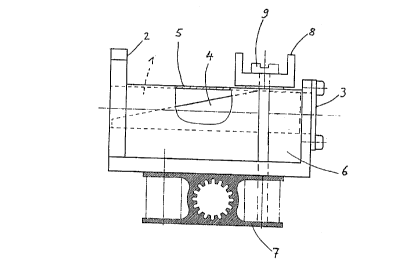
A waveguide absorber which withstands high
mechanical and thermal loads is typified in that a member
(4) exhibiting absorber material is clamped between
waveguide walls (5, 6) in such a way that at least one
wall region (5) adjoining the member (4) is constructed
flexibly, and that a force acting on the flexible wall
region (5) presses the latter against the member (4).


French Abstract

Un absorbeur pour guides d'ondes qui supporte de hautes contraintes mécaniques et thermiques se caractérise par le fait qu'un corps (4) en un matériau absorbant est bloqué entre les parois (5, 6) du guide d'ondes. Au moins une zone (5) de la paroi qui est contre le corps (4) est souple. Une force s'exerçant sur la zone souple (5) de la paroi pousse celle-ci contre le corps (4).

Claims

Note: Claims are shown in the official language in which they were submitted.


THE EMBODIMENTS OF THE INVENTION IN WHICH AN EXCLUSIVE
PROPERTY OR PRIVILEGE IS CLAIMED ARE DEFINED AS FOLLOWS:

1. A waveguide absorber which has at least one member
inserted into a waveguide and exhibiting absorber material,
wherein the member (4) is clamped between waveguide walls (5,
6) by providing that at least one wall region (5) resting on
the member (4) is constructed flexibly, and that a force
acting on the flexible wall region (5) presses the flexible
wall region against the member (4).

2. The waveguide absorber as claimed in claim 1,
wherein the flexible wall region (5) is realized by an
appropriately strong reduction in the wall thickness.

3. The waveguide absorber as claimed in claim 1 or 2,
wherein provision is made of a pressure clamp (8) which exerts
the clamping pressure on the flexible wall region (5), rests
on the flexible wall region (5) and is screwed to a wall
region (6) of the waveguide (1) which is opposite said
flexible wall region.

4. The waveguide absorber as claimed in claim 3,
wherein the clamping pressure is produced by a correspondingly
tight screwing of the pressure clamp (8) to the opposite wall
region (6).

5. The waveguide absorber as claimed in claim 3,
wherein arranged in the pressure clamp (8) are screws which
can be screwed against the flexible wall region (5) in order
to be able to produce the clamping pressure.

Description

Note: Descriptions are shown in the official language in which they were submitted.


Description ~ ~ ~ a ~ 4 7 8 6 4
Waveguide Absorber

The present invention relates to a waveguide absorber which
has at least one member inserted into a waveguide and
exhibiting absorber material.

Non-reflective terminating impedances and attenuators are
frequently required in microwave technology. Use is made as
such of waveguide absorbers such as are disclosed, for
example, in the "Taschenbuch der Hochfrequenztechnik" t"Manual
of Radio-Frequency Technology"], H. Meinke and F. W.
Grundlach, 3rd edition, 1868, pages 443 to 445. This
publication does not reveal the means by which the members
consisting of absorber material and arranged in the waveguide
are fixed.

A waveguide absorber is known from US-A-906,952, in which an
absorbing member is fixed in the waveguide by means of an
adhesive.

Special requirements for fixing the absorbing member are to be
made for the application of waveguide absorbers in the field
of space flight. The fixing is to be able to withstand high
mechanical and thermal loads. It is the object of the present
invention to specify a waveguide absorber of the type
mentioned at the beginning which fulfils the aforementioned
requirements.

According to the invention, this object is achieved by means
of the features of claim 1. Advantageous developments of the
invention follow from the subclaims.

The invention has the advantage that no use is made for fixing
the absorbing member of the usual materials such as adhesive
or solder, which often do not withstand very high thermal or
mechanical stress. In addition, the...


''''.B~

7 ~ 4 7 8 ~ 4 22386-2603

mechanical outlay is very low ln the wavegulde absorber
accordlng to the lnventlon.
The lnvention is explalned below wlth the ald of an
exemplary embodlment represente~ ln the drawlng.
The Flgure above shows a slde vlew of a rectangular
wavegulde 1 whlch ls provlded at one end wlth a flange 2, and
whose other end ls sealed by a cover 3. Inserted lnto thls
wavegulde 1 ls a member 4 whlch conslsts at least


' ~3

3 21~7864
partially of a thermostable absorber material (for
example, silicon carbide). The member 4 extends with a
subregion over the entire height of the waveguide and has
the shape of a wedge. The absorber member can have any
arbitrarily differen~ shape; it depends, ~or example, on
the electrical requirements and on the mounting position
in the waveguide. All that is decisive is that the member
extends at least partially over the entire height of the
waveguide (or the entire diameter of the waveguide in the
case of a round waveguide), so that it can be clamped
between mutually opposite wall regions of the waveguide.
In order to fix the member 4 in the waveguide 1
by clamping, the thickne3s of one waveguide wall S is so
strongly reduced at least in the region resting on the
member 4 that this re~ion is flexible. If a pressure is
exerted on this flexible wall region 5, the member 4 is
pressed against the opposite rigid waveguide wall 6. The
result is a contact, which conducts heat well, between
the member 4 and this waveguide wall 6 on whose outside
a cooling system, for example a heat pipe, is arranged in
accordance with the illustrated exemplary embodiment.
A pressure clamp 8 lying on the flexible wall
region 5 is fastened by means of screws 9 to the opposite
waveguide wall 6. By means of these fastening screws 9
themselves, either the pressure clamp 8 can be tensioned
so far that it exerts the required clamping pressure on
the flexible wall region 5, or it is possible apart from
the fastening screws 9 to provide in addition in the
pressure clamp 8 screws which can be screwed against the
flexible wall region 5.

Representative Drawing
A single figure which represents the drawing illustrating the invention.
Administrative Status

For a clearer understanding of the status of the application/patent presented on this page, the site Disclaimer , as well as the definitions for Patent , Administrative Status , Maintenance Fee  and Payment History  should be consulted.

Administrative Status

Title Date
Forecasted Issue Date 1999-05-11
(86) PCT Filing Date 1993-11-08
(87) PCT Publication Date 1994-05-26
(85) National Entry 1995-04-25
Examination Requested 1995-08-31
(45) Issued 1999-05-11
Expired 2013-11-08

Abandonment History

There is no abandonment history.

Payment History

Fee Type Anniversary Year Due Date Amount Paid Paid Date
Application Fee $0.00 1995-04-25
Maintenance Fee - Application - New Act 2 1995-11-08 $100.00 1995-10-13
Registration of a document - section 124 $0.00 1996-04-04
Maintenance Fee - Application - New Act 3 1996-11-08 $100.00 1996-10-28
Maintenance Fee - Application - New Act 4 1997-11-10 $100.00 1997-07-28
Maintenance Fee - Application - New Act 5 1998-11-09 $150.00 1998-07-31
Final Fee $300.00 1999-02-10
Maintenance Fee - Patent - New Act 6 1999-11-08 $150.00 1999-09-03
Maintenance Fee - Patent - New Act 7 2000-11-08 $150.00 2000-10-25
Maintenance Fee - Patent - New Act 8 2001-11-08 $150.00 2001-10-22
Maintenance Fee - Patent - New Act 9 2002-11-08 $150.00 2002-10-18
Maintenance Fee - Patent - New Act 10 2003-11-10 $200.00 2003-10-29
Maintenance Fee - Patent - New Act 11 2004-11-08 $250.00 2004-10-18
Maintenance Fee - Patent - New Act 12 2005-11-08 $250.00 2005-10-18
Maintenance Fee - Patent - New Act 13 2006-11-08 $250.00 2006-10-18
Maintenance Fee - Patent - New Act 14 2007-11-08 $250.00 2007-10-18
Maintenance Fee - Patent - New Act 15 2008-11-10 $450.00 2008-10-28
Maintenance Fee - Patent - New Act 16 2009-11-09 $450.00 2009-10-26
Maintenance Fee - Patent - New Act 17 2010-11-08 $450.00 2010-10-25
Maintenance Fee - Patent - New Act 18 2011-11-08 $450.00 2011-10-26
Maintenance Fee - Patent - New Act 19 2012-11-08 $450.00 2012-10-25
Owners on Record

Note: Records showing the ownership history in alphabetical order.

Current Owners on Record
ANT NACHRICHTENTECHNIK GMBH
Past Owners on Record
DAMASCHKE, JUERGEN
GEISSLER, KLAUS H.
WOLK, DIETER
Past Owners that do not appear in the "Owners on Record" listing will appear in other documentation within the application.
Documents

To view selected files, please enter reCAPTCHA code :


To view images, click a link in the Document Description column. To download the documents, select one or more checkboxes in the first column and then click the "Download Selected in PDF format (Zip Archive)" or the "Download Selected as Single PDF" button.

List of published and non-published patent-specific documents on the CPD .

If you have any difficulty accessing content, you can call the Client Service Centre at 1-866-997-1936 or send them an e-mail at CIPO Client Service Centre.


Document
Description 
Date
(yyyy-mm-dd) 
Number of pages   Size of Image (KB) 
Cover Page 1999-05-04 1 36
Representative Drawing 1999-05-04 1 9
Cover Page 1995-08-08 1 18
Abstract 1994-05-26 1 12
Description 1994-05-26 2 89
Claims 1994-05-26 1 35
Drawings 1994-05-26 1 16
Description 1998-06-03 3 100
Claims 1998-06-03 1 40
Correspondence 2000-01-11 1 15
Correspondence 1999-02-10 1 38
Fees 1996-10-23 1 44
Fees 1995-10-13 1 47
Prosecution Correspondence 1995-04-25 1 41
Office Letter 1996-04-04 1 27
Office Letter 1995-04-25 1 30
Office Letter 1995-12-08 1 53
Office Letter 1995-11-08 1 40
Correspondence Related to Formalities 1995-11-17 1 46
Office Letter 1998-08-24 1 86
International Preliminary Examination Report 1995-04-25 23 792
Prosecution Correspondence 1995-08-31 1 44
Prosecution Correspondence 1998-04-27 1 40
Prosecution Correspondence 1998-04-09 2 46
Examiner Requisition 1997-12-09 1 38
Prosecution Correspondence 1995-10-11 29 1,906
Prosecution Correspondence 1995-10-11 1 27
Prosecution Correspondence 1995-05-04 1 31
Prosecution Correspondence 1995-04-25 1 26
National Entry Request 1995-04-25 6 200