Note: Descriptions are shown in the official language in which they were submitted.
- 21~7902
- 1 - P12514
BACKGROUND OF THE INVENTION
1. Field of the Invention:
The present invention relates to a gas dis-
charge display apparatus for displaying a character or an
image by light emission utilizing gas discharge which is
for use in an image display apparatus such as a televi-
sion or an advertizing display panel, and a method for
driving the same. In particular, the present invention
relates to a gas discharge apparatus used in the form of
an AC-type plasma display panel (hereinafter, referred to
- as a "PDP") and a method for driving the same.
2. Description of the Related Art:
Gas discharge display apparatuses have a large
display area despite a small depth thereof and realize
color display. For such advantages, use of gas discharge
display apparatuses is now being extended rapidly. Gas
discharge display apparatuses are available in various
types. One type of gas apparatus suitable for image
display is an AC-type PDP. Gas discharge display appara-
tuses of this type, which are disclosed in Japanese Laid-
Open Patent Publication Nos. 59-79938 and 61-39341, and
Japanese Patent Publication No. 62-31775, have a memory
function.
Briefly referring to Figures lA and lB, a
conventional AC-type PDP 1000 will be described. Figure
lA is a plan view of the AC-type PDP 1000, illustrating
an arrangement of electrodes. Figure lB is a cross
sectional view of the AC-type PDP 1000 taken along line
lB-lB' in Figure lA.
2147902
- 2 - P12514
As is shown in Figures lB, the AC-type PDP 1000
includes a first glass substrate 3 and a second glass
substrate 8 opposed to each other. The first glass
substrate 3 and the second glass substrate 8 form an
outer casing of the AC-type PDP 1000 together. On an
inner face of the first glass substrate 3, a first
electrode group including a plurality of scanning elec-
trodes (first discharge electrodes) 1 and a plurality of
sustaining electrodes (second discharge electrodes) 2 is
located. A dielectric layer 4 is located on the first
glass substrate 3, covering the first electrode group,
and a protection layer 5 is located on the dielectric
layer 4. On an inner face of the second glass substrate
8, a second electrode group including a plurality of data
electrodes (third discharge electrodes; also referred to
as "address electrodes") 7 is located.
As is illustrated in Figure lA, the scanning
electrodes la through ln ( only la, lb and lc are shown
here) and the sustaining electrodes 2a through 2n ( only
2a, 2b and 2c are shown here) are provided in parallel
alternately. The data electrodes 7a through 7m ( only 7a
and 7b are shown here) are provided in parallel so as to
perpendicularly cross the scanning electrodes la through
ln and the sustaining electrodes 2a through 2n. Adjacent
scanning electrode and sustaining electrode (for example,
la and 2a) form a pair. A projecting area of the scan-
ning electrode and a projecting area of the sustaining
electrode forming a pair are opposed to each other in an
area S (Figure lA), where sustaining discharge occurs.
The area S will be referred to as a "discharge area".
The second electrode group including the data
2147902
P12514
electrodes 7a through 7m is opposed to the protection
layer 5 with a discharge space 6 full of discharge gas
interposed therebetween. The dielectric layer 4 is
formed of borosilicate glass or the like, and the
protection layer 5 is formed of MgO or the like.
As is illustrated in Figure 2, the scanning
electrodes la through ln, the sustaining electrodes la
through ln, and the data electrodes la through lm are
arranged orthogonally in a lattice. The scanning elec-
trodes la through ln are connected to a scanning elec-
trode driving circuit 10, the sustaining electrodes 2a
through 2n are connected to a sustaining electrode
driving circuit 11, and the data electrodes 7a through 7m
are connected to a data electrode driving circuit 12.
Another conventional AC-type PDP 2000 will be
described with reference to Figures 3A and 3B. Figure 3A
is a plan view of the AC-type PDP 2000, illustrating an
arrangement of electrodes, and Figure 3B is a cross
sectional view of the AC-type PDP 2000 taken along line
3B-3B' in Figure 3A. In Figure 3A, the letter P denotes
a pixel area, and letter S denotes a discharge area. In
Figures 3A and 3B, the same elements as those in Figures
lA and lB bear the same reference numerals therewith.
As is illustrated in Figure 3B, the AC-type PDP
2000 includes three types of phosphor layers R, G and B
for emitting light of red, green and blue which are
located on the inner face of the second glass substrate
8 in order to perform a color display. The phosphor
layers R, G and B are located in positional correspon-
dence with discharge areas S shown in Figure lA, and are
2117902
P12514
excited to emit light upon receiving ultraviolet rays
generated by discharge caused in the discharge areas S.
A method for driving such AC-type PDPs 1000 and
2000 is disclosed in, for example, Japanese Patent Publi-
cation No. 62-61278 and Japanese Laid-Open Patent
Publication No. 4-170581. In the latter publication, the
driving method is described as a method for driving a dot
matrix display panel.
With reference to Figure 4, a conventional
method for driving an AC-type (1000 or 2000) PDP will be
described.
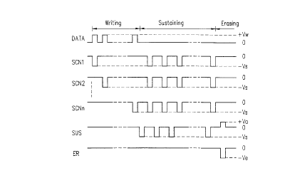
First, in the writing operation performed in a
writing period, a positive writing pulse having an
amplitude of +Vw shown in waveform DATA in Figure 4 is
applied to at least one data electrode selected from the
data electrodes 7a through 7m (for example, the data
eiectrode 7a) which corresponds to a pixel for displaying
an image in accordance with the scanning electrode la.
Simultaneously, a negative scanning pulse having an
amplitude of -Vs shown in waveform SCN1 is applied to the
scanning electrode la. By such application, discharge
occurs at an intersection W1 (Figure lA) of the data
electrode 7a and the scanning electrode la, and thus a
positive charge is stored in an area of a surface of the
protection layer 5, the area positionally corresponding
to the intersection W1. In other words, such an area
acts as a write cell.
Next, a positive writing pulse having an ampli-
2147902
P12514
tude of +Vw shown in waveform DATA is applied to at least
one data electrode selected from the data electrodes 7a
through 7m (for example, the data electrode 7a) which
corresponds to a pixel for displaying an image in
accordance with the scanning electrode lb. Simulta-
neously, a negative scanning pulse having an amplitude of
-Vs shown in waveform SCN2 is applied to the scanning
electrode lb. By such application, discharge occurs at
an intersection W2 (Figure lA) of the data electrode 7a
and the scanning electrode lb, and thus a positive charge
is stored in an area of the surface of the protection
layer 5, the area positionally corresponding to the
intersection W2. In other words, such an area acts as a
write cell.
In this manner, during the process of applying
negative scanning pulses having an amplitude of -Vs shown
in waveforms SCN1 through SCNn to the scanning electrodes
la through ln respectively, a positive writing pulse
having an amplitude of +Vw is applied to at least one
selected data electrode which corresponds to a pixel for
displaying an image in accordance with the respective
scanning electrode. Thus, a positive charge is stored in
a prescribed area (write cell) of the surface of the
protection layer 5.
The writing operation is followed by the
sustaining operation performed in a sustaining period.
In the sustaining operation, a negative sustaining pulse
having an amplitude of -Vs shown in waveform SUS is
applied to all the sustaining electrodes 2, and negative
sustaining pulses having an amplitude of -Vs shown in
waveforms SCN1 through SCNn are applied to all the
2147902
P12514
-- 6 --
scanning electrodes 1, respectively. The pulse applica-
tion to the sustaining electrodes 2 and the pulse
application to the scanning electrodes 1 are performed
alternately. The application of the first sustaining
pulse to each sustaining electrode 2 discharges the
positive charge stored on the protection layer 5, and
thus sustaining discharge occurs on the discharge area S
which belongs to the same discharge cell as the respec-
tive intersection. The alternate application of the
negative sustaining pulse to each sustaining electrode 2
and each scanning electrode 1 continues the sustaining
discharge on the respective discharge area S. By light
emission caused by such sustaining discharge, characters
and images are displayed.
In the erasing operation performed in an
erasing period, a negative erasing pulse having an ampli-
tude of -Ve and a small width t~ shown in waveform SUS is
applied to all the sustaining electrodes 2. (Hereinafter,
a pulse having a small width will be referred to as a
"narrow pulse".) By such application, erasing discharge
occurs, and thus the charge stored on the protection
layer 5 by sustaining discharge is completely erased. As
a result, the sustaining discharge does not continue even
if a sustaining pulse is applied. Thus, the sustaining
operation is terminated.
Conventionally, the erasing pulse applied to
the sustaining electrodes has an absolute value of the
amplitude which is smaller than the that of the sustain-
ing pulse, or has a width smaller than that of the
sustaining pulse. In order to enlarge the margin for the
erasing operation, both of the absolute value of the
-
2147~02
P12514
amplitude and the width of the erasing pulse need to be
smaller than those of the sustaining pulse. Alternative-
ly, a plurality of erasing pulses having small but
different widths may be applied.
In order to stabilize the writing, sustaining
and erasing operations, the rise and fall of each of the
writing, scanning, sustaining and erasing pulses are
applied with steep rise and fall. The time period
required for the change in the voltage at the rise and
fall is generally set to be as short as several hundred
nanoseconds.
The luminance of light obtained by performing
sustaining discharge once is determined by the amplitude
of the sustaining pulse, the capacitance between the
scanning electrodes la through ln and the surface of the
protection layer 5, the capacitance between the sustain-
ing electrodes 2a through 2n and the surface of the
protection layer 5, and the like. However, the amplitude
of each pulse is substantially determined by charac-
teristics of the AC-type PDP and thus cannot be changed
arbitrarily. The structure of the AC-type PDP, the
material of the electrodes, the type of the discharge
gas, the sealing pressure and the like cannot be changed
after the AC-type PDP is produced. Accordingly, the
luminance of light can be controlled simply by changing
the number of times the sustaining discharges is repeated
(namely, the number of pulses) per time unit.
Next, the above-described operations will be
described in detail with reference to Figures 5A through
5G. Figures 5A through 5G illustrate existing and moving
- 2147902
- 8 - P12514
states of the wall charges in a discharge cell in each
step of the above-described operations.
Figures 5A through 5G are cross sectional views
of a conventional AC-type PDP which is similar to the AC-
type PDPs shown in Figures lB and 3B. In Figures 5A
through 5G, the data electrode 7 on the inner face of the
second glass substrate 8 is covered with a second
dielectric layer 9, and the phosphor layers R, G and B
(only R is shown in Figure 5A) are located on the second
dielectric layer 9. The AC-type PDP illustrated in
Figures 5A through 5G has the same structure as the
structure of the AC-type PDPs 1000 and 2000 shown in
Figures lB and 3B except for the above-described points.
The same elements as in the AC-type PDPs 1000 and 2000
bear the same reference numerals therewith.
Figure 5A shows an initial state before the AC-
type PDP is turned on. The discharge cell of the AC-type
PDP has no wall charge.
As is shown in Figure 5B, in the writing period
after the AC-type PDP is turned on, a writing pulse
having an amplitude of +Vw (V) is applied to the data
electrode 7 and a negative scanning pulse having an
amplitude of -Vs (V) is applied to the scanning electrode
1. Then, writing discharge occurs at the intersection of
the data electrode 7 and the scanning electrode 1. A
negative wall charge is stored in an area of a surface of
the second dielectric layer 9 corresponding to the data
electrode 7, and a positive wall charge is stored in an
area of the surface of the protection layer 5 correspond-
ing to the scanning electrode 1.
2147902
P12514
As is shown in Figure 5C, in the sustaining
period, a negative sustaining pulse having an amplitude
of -Vs (V) is applied to the sustaining electrode 2.
Thus, a positive wall charge is stored in an area of the
surface of the protection layer 5 corresponding to the
sustaining electrode 1. The voltage generated by the
positive wall charge is superimposed on the voltage of
the sustaining pulse and applied between the area of the
surface of the protection layer 5 corresponding to the
scanning electrode 1 and the area of the protection layer
5 corresponding to the sustaining electrode 2. Accord-
ingly, sustaining discharge occurs between the above-
mentioned two areas. As a result, a negative wall charge
is stored on the area of the protection layer 5 corre-
sponding to the scanning electrode 1, and a positive wallchange stored on the area of the protection layer 5
corresponding to the sustaining electrode 2.
Further in the sustaining period, as is shown
in Figure 5D, a negative sustaining pulse having an
amplitude of -Vs (V) is applied to the scanning electrode
1. Then, the voltage generated by the negative wall
charge stored on the area of the protection layer 5
corresponding to the scanning electrode 1 by the
sustaining discharge and the voltage generated by the
positive wall charge stored on the area of the protection
layer 5 corresponding to the sustaining electrode 2 are
superimposed on the voltage of the sustaining pulse and
applied between the area of the protection layer 5
corresponding to the scanning electrode 1 and the area of
the protection layer 5 corresponding to the sustaining
electrode 2. Thus, sustaining discharge occurs again
between the above-mentioned two areas but in the opposite
- 21~7902
P12514
- 10 -
direction. As a result, a negative wall charge is stored
on the area of the protection layer 5 corresponding to
the sustaining electrode 2, and a positive wall charge is
stored on the area of the protection layer 5 correspond-
ing to the scanning electrode 1.
Still further in the sustaining period, as isshown in Figure 5C again, a negative sustaining pulse
having an amplitude of -Vs (V) is applied to the sustain-
ing electrode 2. Then, the voltage generated by thenegative wall charge stored on the area of the protection
layer 5 corresponding to the sustaining electrode 2 by
the sustaining discharge and the voltage generated by the
positive wall charge stored on the area of the protection
layer 5 corresponding to the scanning electrode 1 are
superimposed on the voltage of the sustaining pulse and
applied between the area of the protection layer 5
corresponding to the scanning electrode 1 and the area of
the protection layer 5 corresponding to the sustaining
electrode 2. Accordingly, sustaining discharge occurs
again between the above-mentioned two areas. As a
result, a negative wall charge is stored on the area of
the protection layer corresponding to the scanning elec-
trode 1, and a positive wall charge is stored on the area
of the protection layer 5 corresponding to the sustaining
electrode 2.
In this manner, sustaining discharge (movement
of charges) occurs repeatedly in the sustaining period as
is shown in Figures 5C and 5D, and the phosphor layers R,
G and B are excited by ultraviolet rays generated by the
repeated sustaining discharge, thereby performing dis-
play.
-- 2147902
- 11 - P12514
As is shown in Figure 5E, in the erasing
period, a negative narrow erasing pulse having an
amplitude of -Vs (V) is applied to the sustaining elec-
trode 2. Then, the voltage generated by the negative
wall charge stored on the area of the protection layer 5
corresponding to the sustaining electrode 2 by the sus-
taining discharge and the voltage generated by the posi-
tive wall charge stored on the area of the protection
layer 5 corresponding to the scanning electrode 1 are
superimposed on the voltage of the negative narrow erasi-
ng pulse and applied between the area of the protection
layer 5 corresponding to the scanning electrode 1 and the
area of the protection layer 5 corresponding to the
sustaining electrode 2. Accordingly, erasing discharge
occurs again between the above-mentioned two areas.
However, since such erasing discharge is maintained for
a short period of time due to the narrow pulse, the
discharge is terminated midway. Accordingly, by setting
the width of the narrow erasing pulse to be optimum, the
wall charge on the area of the protection layer corre-
sponding to the sustaining electrode 1 and the wall
charge on the area of the protection layer 5 correspond-
ing to the scanning electrode 2 can be neutralized.
Thereafter, sustaining discharge does not occur even if
a sustaining pulse is applied unless a writing pulse is
applied again. Accordingly, discharge is kept in a
pause. The level of the residual wall charge in Figure
5E is less than the level of the residual wall charge in
Figure 5B because the wall charge is partially extin-
guished during the sustaining discharge.
As is shown in Figure 5F, in the writingperiod, a positive pulse having an amplitude of +Vw (V)
- 2147902
P12514
- 12 -
is applied to the data electrode 7 and a negative scan-
ning pulse having an amplitude of -Vs (V) is applied to
the scanning electrode 1. Then, writing discharge occurs
between an area of the second dielectric layer 9 corre-
sponding to the data electrode 7 and the area of theprotection layer 5 corresponding to the scanning elec-
trode 1. By such writing discharge, a negative wall
charge is stored on the area of the second dielectric
layer 9 corresponding to the data electrode 7, and a
positive wall charge is stored on the area of the second
dielectric layer 9 corresponding to the scanning elec-
trode 1 in addition to the residual wall charge shown in
Figure 5E. As a result, the level of the charge in
Figure 5E becomes equal to the level of the charge in
Figure 5B. By repeating the operation illustrated in
Figures 5F, 5C, 5D and 5E in this manner, an image is
displayed.
In the above-described conventional example, a
method for driving the AC-type PDP in which the date
electrodes 7 are covered with the second dielectric layer
9 and phosphor layers R, G and B are provided on the
second dielectric layer 9 is described. The same method
can be used for driving an AC-type PDP in which display
is performed directly utilizing light emitted by dis-
charge and thus has no phosphor layer. The same method
can also be used for driving an AC-type PDP in which the
data electrodes 7 are directly covered with a phosphor
layer without the second dielectric layer 9. In such a
case, the phosphor layer acts in the same manner as the
second dielectric layer 9. The same method can still be
used for driving an AC-type PDP in which the data elec-
trodes 7 are exposed to the discharge space 6 without the
-
2147~02
P12514
- 13 -
second dielectric 9 or the phosphor layer. In such acase, although no wall charge is stored on the area of
the second dielectric layer 9 corresponding to the data
electrodes 7, an equivalent wall charge is stored on the
area of the protection layer 5 corresponding to the
scanning electrode 1.
A conventional scanning electrode driving
circuit 30 will be described with reference to Figures 6
and 7. Figure 6 is a circuit diagram of the scanning
electrode driving circuit 30. The scanning electrode
driving circuit 30 includes p-channel MOSFETs 13 with-
standing a high voltage and n-channel MOSFETs 14 also
withstanding a high voltage. The p-channel MOSFETs 13
are respectively connected to scanning electrodes la
through ln through a drain electrode thereof, and the n-
channel MOSFETs 14 are also respectively connected to
scanning electrodes la through ln through a drain elec-
trode thereof. A source of each p-channel MOSFET 13 is
grounded, and a source of each n-channel MOSFET 14 is
connected to a high voltage power source of -200 V. Each
p-channel MOSFET 13 and each n-channel MOSFET 14 form an
output section of a push-pull system withstanding a high
voltage.
The p-channel MOSFETs 13 are connected to a
scanning logic circuit 16 via a level shift (L/S) circuit
15 withstanding a high voltage, and the n-channel MOSFETs
14 are directly connected to the scanning logic circuit
16.
The scanning logic circuit 16 includes a shift
register 17, a first gate 18, a second gate 19 and an
- 21~7902
P12514
- 14 -
inverter 20. A common line which is the basis for asignal level in the scanning logic circuit 16 is connect-
ed to the high voltage power source of -200 V.
Figure 7 is a timing chart illustrating opera-
tion in the scanning electrode driving circuit 30.
When a scanning data signal SI and a clock
signal CLK are input to the shift register 17, the
scanning data signal SI is taken in at the falling edge
of the clock signal CLK. The level of outputs from the
shift register 17 becomes low one by one, and a scanning
signal is output. Only while the level of a blanking
signal BLK is low, the scanning signal passes through the
first gate 18, the second gate 19, the inverter 20, and
the level shift circuit 15 and is applied to each p-
channel MOSFET 13 and each n-channel MOSFET 14. Thus, a
scanning pulse is applied to the scanning electrode la
through ln one by one.
In the sustaining period, when a sustaining
signal SU, is input to the second gate 19, a sustaining
pulse is applied to all the scanning electrodes la
through ln simultaneously.
Conventionally, in order to reduce the size of
the scanning electrode driving circuit 30 illustrated in
Figure 6, the scanning electrode driving circuit 30 is
divided into an appropriate number of blocks to form a
monolithic IC.
The conventional AC-type PDPs which are de-
scribed above have the following problems.
- 21~7902
- 15 - P12514
(1) The conditions for setting the erasing
operation are stringent as is described above. If the
conditions are set inappropriately, right image
reproduction cannot be performed due to the influence of
the residual charge. The potential in the discharge area
S is dispersed easily by different discharge cells, and
discharge characteristics change over time.
In addition, since the width of the erasing
pulse is small, the start of erasing discharge can be
delayed by fluctuation in the width of the erasing pulse
when the erasing pulse is applied. In such a case, the
charge stored in the discharge area S cannot be erased
completely.
In detail, the tolerance for the fluctuation in
the width tw~ and the amplitude -Ve of the erasing pulse
cannot be large. Accordingly, if the characteristics are
dispersed in different discharge cells, erasing discharge
can be performed excessively or insufficiently in some
discharge cells. Since the charge stored on the protec-
tion layer 5 is not completely erased in such discharge
cells, a sufficient margin for erasing operation cannot
be obtained. Excessive erasing discharge means that,
after the charge stored on the protection layer 5 is
erased, a charge having an opposite polarity is stored.
Insufficient erasing discharge means that the charge
stored on the protection layer 5 cannot be reduced to
zero.
(2) When the positive charge stored on the area
of the protection layer 5 corresponding to the intersec-
tion (for example, W1 or W2 in Figure lA) of a scanning
214790~
P12514
- 16 -
electrode and a data electrode moves to the dischargearea S, the level of the charge moving to sub-area Sl is
different from the level of the charge moving to sub-area
S2 because sub-area S1 is closer to the intersection W1
than sub-area S2. Accordingly, the charge distribution
in the discharge area S is not uniform. As a result,
when an erasing pulse is applied, the level of the charge
is non-uniform in the area of the protection layer 5
corresponding to the discharge area S. Thus, the erasing
operation cannot be uniform in the entire discharge area
S.
(3) In the case of color display, if the widths
of the scanning electrodes and the sustaining electrodes
opposed to each other in the discharge area S are reduced
in order to obtain a pixel area P which is substantially
square, the discharge area S is also reduced. As a
result, sufficient luminance cannot be obtained especial-
ly in a large color display apparatus.
(4) Even when the discharge is set to be
performed 60 times per second as is generally done in a
personal computer, a television and the like, the lumi-
nance is excessively high when the efficiency of the AC-
type PDP is high. Under the circumstances, images can bedisplayed at a high luminance but not at a low luminance.
(5) Discharge current flowing during the
sustaining period concentrates when the level of the
sustaining pulse is changed as is shown in Figure 4.
Accordingly, the peak value Ip of the discharge current
is excessively large compared with the average value Ia.
2147902
- 17 - P12514
As a result, the circuit for supplying a power source
requires a capacitor having a large capacity for smooth-
ing the current and a switching transistor for supplying
a large peak current. Further, in order to prevent an
adverse effect of noise generated by such a large peak
current on the circuit operation, a noise removal circuit
and a multiple-layer substrate~are required.
(6) In the conventional scanning electrode
driving circuit 30, an output section of a push-pull
system withstanding a high voltage including the p-
channel MOSFET 13 and the n-channel MOSFET 14 is required
for each of the scanning electrodes la through ln. The
level shift circuit 15 withstanding a high voltage is
also required. Accordingly, incorporation of the scan-
ning electrode driving circuit 30 into an IC is diffi-
cult. Even if the scanning electrode driving circuit 30
is incorporated into an IC, the chip area is sufficiently
large to raise production cost. If a shortcircuit occurs
between the scanning electrodes la through ln, the
scanning electrode driving circuit 30 breaks down.
(7) The writing operation shown in Figure 5F
requires writing discharge caused in the state where the
residual wall charge remains after the erasing period
shown in Figure 5E is terminated. However, the residual
wall charge acts in the direction to counteract the
voltage of the writing pulse, writing discharge is more
difficu1t to be realized when compared with the state
shown in Figure 5B. Even if writing discharge occurs,
the difference between the wall charge on the area of the
protection layer 5 corresponding to the scanning elec-
trode 1 and the wall charge on the area of the protection
- 2147902
P12514
- 18 -
layer 5 corresponding to the sustaining electrode 2 istoo small to easily start sustaining discharge. As a
result, no light is emitted in some discharge cells.
In the case that the AC-type PDP is turned on
to start operating in the state where the wall charge has
already been distributed as is shown in Figure 5G,
namely, in the state where a negative wall charge is
stored on the area of the second dielectric layer 9
corresponding to the data electrodes 7 and a positive
wall charge is stored on the area of the protection layer
5 corresponding to the scanning electrodes 1 and the
sustaining electrodes 2, the wall charges act in a direc-
tion counteracting the voltage of the writing pulse.
Accordingly, writing discharge and sustaining discharge
are both difficult to occur, and the discharge operation
is not performed until the wall charges shown in Figure
5G are naturally extinguished. As a result, the rising
time for the display after the AC-type PDP is turned on,
namely, the time period which is required for the AC-type
PDP to perform normal display after the AC-type PDP is
turned on is extended.
Figure 8 is a plan view of a conventional image
display panel 40 such as a PDP, a liquid crystal display
(LCD) panel, a panel using an electroluminescent lamp
(EL), or a panel using a fluorescent display tube. As is
illustrated in Figure 8, such a panel includes a flat
casing 21 having a rectangular front wall 22. An image
display area DA is set on the rectangular front wall 22.
Inside the flat casing 21, electrodes for display are
sealed. The front wall 22 is formed of a glass plate. A
2147902
P12514
-- 19 --
mosaic-like large display screen is formed by arranging
a plurality of such image display panels 40 in a lattice,
in a plurality of lines and a plurality of columns. Such
a large display screen is used for a television or an
advertising display panel.
In forming a large display screen by a plurali-
ty of such image display panels 40, the panels 40 are
arranged two dimensionally so that there is no gap
between two adjacent panels 40. However, since the front
wall 22 is formed of glass, a non-display area 23 shaped
as a rectangular frame and surrounding each image display
panel 40, namely, a side wall of the flat casing 21 and
the sealing material such as frit glass, appear through
the front wall 22. Accordingly, such a non-display area
23 inevitably appears on the large display screen as non-
light emitting dark lines in a lattice. Such a lattice
significantly spoil the display quality.
In the case when one image display panel 40 has
only a small number of pixels, for example, two, the dark
lines are not very disturbing from far since the lines
are scattered on the large display screen. However,
display devices which are used for a high precision image
display apparatus and an image display apparatus for
indoor use, a great number of pixels are used at a high
density. In such a state, the junction between two
adjacent image display panel 40 is conspicuous as a dark
lattice, and moreover the reproduced image is distorted.
SUMMARY OF THE INVENTION
In one aspect of the present invention, a gas
- 2147902
P12514
- 20 -
discharge display apparatus includes a first substrateand a second substrate located opposed to each other with
a discharge space interposed therebetween to form an
outer casing; a first electrode group including a plural-
ity of scanning electrodes and a plurality of sustainingelectrodes located parallel to each other on an inner
face of the first substrate, each of the plurality of
scanning electrodes and each of the plurality of sustain-
ing electrodes forming a pair; a dielectric layer cover-
ing the first electrode group; and a second electrodegroup including a plurality of data electrodes and a
plurality of erasing electrodes located parallel to each
other on an inner face of the second substrate in a
direction perpendicular to the first electrode group,
each of the plurality of data electrodes and each of the
plurality of erasing electrodes forming a pair.
In another aspect of the present invention, a
method for driving a gas discharge display apparatus
includes the steps of applying a voltage pulse to the
plurality of scanning electrodes and the plurality of
sustaining electrodes included in the first electrode
group alternately, thereby causing sustaining discharge
between each pair of scanning electrode and sustaining
electrode; and causing erasing discharge between the
plurality of sustaining electrodes and the plurality of
erasing electrodes, thereby erasing a residual charge.
In still another aspect of the present inven-
tion, a gas discharge display apparatus includes a firstsubstrate and a second substrate located opposed to each
other with a discharge space interposed therebetween to
form an outer casing; a first electrode group including
2147902
- 21 - P12514
a plurality of scanning electrodes and a plurality of
sustaining electrodes located on an inner face of the
first substrate, each of the plurality of scanning
electrodes and each of the plurality of sustaining
electrodes forming a pair; a dielectric layer covering
the first electrode group; and a second electrode group
including a plurality of data electrodes located on an
inner face of the second substrate parallel to one
another in a direction perpendicular to the first elec-
trode group. The plurality of scanning electrodes andthe plurality of sustaining electrodes each have a comb-
like shape with teeth. The scanning electrode and the
sustaining electrode in each pair are opposed to each
other with a small gap interposed therebetween in the
manner that the teeth thereof are in engagement with each
other. The plurality of data electrodes are located
opposed to and in a longitudinal direction of the teeth
of the plurality of scanning electrodes.
In one embodiment of the invention, the second
electrode group includes a plurality of erasing elec-
trodes located parallel to the plurality of data elec-
trodes, respectively.
In one embodiment of the invention, the
plurality of erasing electrodes are formed of a cathode
material.
In still another aspect of the present inven-
tion, a gas discharge display apparatus includes a first
substrate and a second substrate located opposed to each
other with a discharge space interposed therebetween to
form an outer casing; a first electrode group including
- 2147902
P12514
- 22 -
a plurality of scanning electrodes and a plurality ofsustaining electrodes located parallel to each other on
an inner face of the first substrate, each of the plural-
ity of scanning electrodes and each of the plurality of
sustaining electrodes forming a pair; a dielectric layer
covering the first electrode group; and a second elec-
trode group including a plurality of data electrodes
located parallel to one another on an inner face of the
second substrate in a direction perpendicular to the
first electrode group. At least one of the plurality of
scanning electrodes and the plurality of sustaining
electrodes are each divided into a plurality of areas,
and terminals respectively connected to the areas are
drawn outside the outer casing.
In still another aspect of the present inven-
tion, a method for driving a gas discharge display
apparatus includes the step of dividing at least one of
the plurality of scanning electrodes and the plurality of
sustaining electrodes into a plurality of groups, and
applying pulses having different phases to the at least
one of the plurality of scanning electrodes and the
plurality of sustaining electrodes in different groups,
thereby causing sustaining discharge.
In still another aspect of the present inven-
tion, a method for driving a gas discharge display
apparatus includes the step of applying an erasing pulse
having an instantaneous voltage which changes slowly in
one of an increasing manner and a decreasing manner to at
least one of the plurality of scanning electrodes and the
plurality of sustaining electrodes, thereby increasing a
voltage between the scanning electrodes and the sustain-
~- 2147902
P12514
- 23 -
ing electrodes slowly to perform an erasing operation.
In one embodiment of the invention, a timeperiod required for the instantaneous voltage of the
erasing pulse to change between 10% and 90% of an ampli-
tude thereof is set to be between 10 ~s and 10 ms inclu-
sive.
In still another aspect of the present inven-
tion, a gas discharge display apparatus includes aplurality of data electrodes; a plurality of scanning
electrodes located in a direction perpendicular to the
plurality of data electrodes; a plurality of switching
devices withstanding a high voltage, the switching
devices respectively having first main electrodes which
are connected to the plurality of scanning electrodes
respectively and independently; a plurality of reverse
conductive diodes connected in parallel to the plurality
of switching devices, respectively; a scanning logic
circuit connected to a control electrode of each of the
plurality of switching devices; and a push-pull circuit
withstanding a high voltage which has an output connected
to a second main electrode of each of the plurality of
switching devices and to a common line which is the basis
of the signal level in the scanning logic circuit.
In one embodiment of the invention, the plural-
ity of switching devices are each an n-channel MOSFET
withstanding a high voltage, and the plurality of reverse
conductive diodes are each a parasitic diode formed in
each n-channel MOSFET.
In one embodiment of the invention, the plural-
2147902
P12514- 24 -
ity of switching devices are each an npn bipolar transis-
tor withstanding a high voltage.
In still another aspect of the present inven-
tion, a method for driving a gas discharge displayapparatus includes a writing step of applying a writing
pulse to the plurality of data electrodes and applying a
scanning pulse having an opposite polarity to the polari-
ty of the writing pulse to the plurality of scanning
electrodes; a sustaining step of applying a sustaining
pulse to the plurality of sustaining electrodes and the
plurality of scanning electrodes; and an erasing step of
applying an erasing pulse. Prior to the writing step,
the initiating step is performed of applying an initiat-
ing pulse having a prescribed polarity to prescribedelectrodes selected from the group consisting of the
plurality of data electrodes, the plurality of sustaining
electrodes and the plurality of scanning electrodes.
In one embodiment of the invention, the
initiating step includes the step of applying an
initiating pulse having an opposite polarity to the
polarity of the scanning pulse applied in the writing
step to at least one of the plurality of scanning elec-
trodes and the plurality of sustaining electrodes.
In one embodiment of the invention, the
initiating step includes the step of applying an
initiating pulse having an opposite polarity to the
polarity of the writing pulse applied in the writing step
to the plurality of data electrodes.
In one embodiment of the invention, a time
-
-- 2147902
- 25 - Pl2514
period required for the instantaneous voltage of the
initiating pulse to change between 10% and 90% of an
amplitude thereof is set to be between 5 ,us and 10 ms
inclusive.
In one embodiment of the invention, the
initiating step includes the step of applying an assist-
ing pulse, to the plurality of scanning electrodes and
the plurality of sustaining electrodes, having an identi-
cal polarity and an identical amplitude with the polarityand the amplitude of the initiating pulse to the plurali-
ty of data electrodes.
In one embodiment of the invention, the
initiating step includes the step of applying an assist-
ing pulse, to the plurality of data electrodes, having an
identical polarity and an identical amplitude with the
polarity and the amplitude of the initiating pulse to the
plurality of scanning electrodes and the plurality of
sustaining electrodes.
In one embodiment of the invention, a time
period required for the instantaneous voltage of the
assisting pulse to change between 10% and 90% of an
amplitude thereof is set between 5 ,us and 10 ms inclu-
sive.
In still another aspect of the present inven-
tion, an image display apparatus includes a large screen
including a plurality of image display panels arranged
two dimensionally, the plurality of image display panels
each including a plurality of display units in a plurali-
ty of lines and a plurality of columns, the plurality of
2147902
Pl2514
- 26 -
display units each acting as a pixel. The plurality ofdisplay units are arranged at an equal distance in a
direction of the lines and a direction of the columns in
each of the plurality of image display panels, and the
display unit in a peripheral area of the corresponding
image display panel which is most proximate to the
adjacent image display panel is shorter than the other
display units in at least one of the direction of the
lines and the direction of the columns.
In still another aspect of the present inven-
tion, an image display apparatus includes an image
display panel including a flat outer casing having a
rectangular light-transmitting front wall and electrodes
for display sealed in the image display panel, the image
display panel further having an image display area
surrounded by a non-display area having a shape of a
rectangular frame and set on the front wall; and a
rectangular transparent plate laminated on an outer face
of the front wall. An outer periphery of a front face of
the transparent plate corresponding to the non-display
area has such a shape as to allow the outer periphery to
act as a lens.
Thus, the invention described herein makes
possible the advantages of (1) providing a gas discharge
display apparatus for performing the erasing operation
with certainty and a method for driving the same, (2)
providing a gas discharge display apparatus for realizing
both of an image of a high luminance and an image of a
low luminance efficiently and a method for driving the
same, (3) providing a method for driving a gas discharge
display apparatus for reducing the peak value of the
- 2147~02
P12514
- 27 -
discharge current during a sustaining period, (4) provid-
ing a method for driving a gas discharge display appara-
tus for supplying a sufficiently large tolerance for the
fluctuation of the width and the amplitude of an erasing
pulse to obtain a sufficient margin for the erasing
operation even if the characteristics are dispersed in
different discharge cells, (5) providing a gas discharge
display apparatus equipped with a driving circuit which
is easily incorporated into an IC and which avoids break-
down even if a shortcircuit occurs between scanning elec-
trodes, (6) providing a method for driving a gas dis-
charge display apparatus for shortening the rising time
of the gas discharge display apparatus for display after
the apparatus is turned on and preventing generation of
a discharge cell where no light emission occurs, and (7)
providing a gas discharge display apparatus for which the
mosaic-like large display screen is not visually influ-
enced in an unfavorable manner by a non-display area of
each of a great number of image display panels which are
arranged in a lattice at a high density to form the large
display screen and thus images are displayed with no
distortion.
These and other advantages of the present
invention will become apparent to those skilled in the
art upon reading and understanding the following detailed
description with reference to the accompanying figures.
BRIEF DESCRIPTION OF THE DRAWINGS
Figure lA is a plan view of a conventional AC-
type PDP, illustrating an arrangement of electrodes.
2147902
P12514
- 28 -
Figure lB is a cross sectional view of the AC-
type PDP in Figure lA taken along line lB-lB' in Figure
lA.
Figure 2 is a schematic view illustrating the
arrangement of the electrodes in the conventional AC-type
PDP in Figure lA.
Figure 3A is a plan view of another convention-
al AC-type PDP, illustrating an arrangement of elec-
trodes.
Figure 3B is a cross sectional view of the AC-
type PDP in Figure 3B taken along line 3B-3B' in Figure
3A.
Figure 4 is a timing chart illustrating a
method for driving a conventional AC-type PDP.
Figures 5A through 5G are cross sectional views
of a conventional AC-type PDP, illustrating the existing
and moving state of charges in a discharge cell while the
AC-type PDP is operating.
Figure 6 is a circuit diagram for a convention-
al scanning electrode driving circuit.
Figure 7 is a timing chart illustrating opera-
tion of the scanning electrode driving circuit shown in
Figure 6.
Figure 8 is a plan view of a conventional image
display panel.
-- 2147902
P12514
- 29 -
Figure 9A is a partial plan view of an AC-type
PDP in a first example according to the present inven-
tion, illustrating an arrangement of electrodes.
Figure 9B is a cross sectional view of the AC-
type PDP in Figure 9A taken along line 9B-9B' in Figure
9A.
Figure 9C is a cross sectional view of the AC-
type PDP in Figure 9A taken along line 9C-9C' in Figure
9A.
Figures 10A and 10B are timing charts illus-
trating a method for driving the AC-type PDP shown in
Figure 9A.
Figure 11A is a partial plan view of an AC-type
PDP in a second example according to the present inven-
tion, illustrating an arrangement of electrodes.
Figure 11B is a cross sectional view of the AC-
type PDP in Figure 11A taken along line 11B-11B' in
Figure 11A.
Figure 12 is a timing chart illustrating a
method for driving the AC-type PDP in Figure 11A.
Figure 13A is a partial plan view of an AC-type
PDP in a modification of the second example, illustrating
an arrangement of electrodes.
Figure 13B is a cross sectional view of the AC-
type PDP in Figure 13A taken along line 13B-13B' in
21 4790~
P12514
- 30 -
Figure 13A.
Figure 14A is a partial plan view of an AC-type
PDP in another modification of the second example,
illustrating an arrangement of electrodes.
Figure 14B is a cross sectional view of the AC-
type PDP in Figure 14A taken along line 14B-14B' in
Figure 14A.
Figure 15A is a partial plan view of an AC-type
PDP in still another modification of the second example,
illustrating an arrangement of electrodes.
Figure 15B is a cross sectional view of the AC-
type PDP in Figure 15A taken along line 15B-15B' in
Figure 15A.
Figure 16A is a partial plan view of an AC-type
PDP, illustrating an arrangement of electrodes.
Figure 16B is a cross sectional view of the AC-
type PDP in Figure 16A taken along line 16B-16B' in
Figure 16A.
Figure 17A is a partial plan view of an AC-type
PDP in a third example according to the present inven-
tion, illustrating an arrangement of electrodes.
Figure 17B is a cross sectional view of the AC-
type PDP in Figure 17A taken along line 17B-17B' in
Figure 17A.
21 47902
P12514
- 31 -
Figure 18 is a timing chart illustrating amethod for driving an AC-type PDP in a fourth example
according to the present invention.
Figure 19 is a timing chart illustrating a
method for driving an AC-type PDP in a modification of
the fourth example.
Figure 20 is a timing chart illustrating a
method for driving an AC-type PDP in a fifth example
according to the present invention.
Figure 21 is a graph illustrating discharge
characteristics of an AC-type PDP with respect to a time
period required for the voltage of an erasing pulse to
change between certain levels.
Figure 22 is a diagram showing an erasing
circuit for generating an erasing pulse in the fifth
example.
Figures 23A, 23B and 23C are timing charts
illustrating different methods for applying an erasing
pulse in various modifications of the fifth example.
Figure 24 is a circuit diagram of a scanning
electrode driving circuit in a sixth example according to
the present invention.
Figure 25 is a timing chart illustrating a
method for driving the scanning electrode driving circuit
shown in Figure 24.
~ 2147902
P12514
- 32 -
Figure 26 is a diagram of a scanning electrodedriving circuit in a modification of the sixth example.
Figure 27 is a timing chart illustrating a
method for driving an AC-type PDP in a seventh example
according to the present invention.
Figures 28A through 28G are cross sectional
views of an AC-type PDP, illustrating the existing and
moving state of charges in a discharge cell while the AC-
type PDP is operating in the seventh example.
Figure 29A is a timing chart illustrating a
method for applying an initiating pulse in a modification
of the seventh example.
Figure 29B is a cross sectional view illustrat-
ing the state of an electrode supplied with an initiating
pulse shown in Figure 29A.
Figures 30A and 30B are timing charts illus-
trating a method for applying an initiating pulse in
other modifications of the seventh example.
Figure 31 is a graph illustrating discharge
characteristics of the AC-type PDP in the seventh example
with respect to a time period required for the voltage of
an initiating pulse to change between certain levels.
Figures 32A and 32B are timing charts illus-
trating a method for applying an initiating pulse in
other modifications of the seventh example.
.
- 2147902
P12514
Figures 33A and 33B are timing charts illus-
trating a method for applying an initiating pulse in
still other modifications of the seventh example.
Figure 34 is a timing chart illustrating a
method for driving an AC-type PDP in still another
modification in the seventh example.
Figure 35 is a timing chart illustrating a
method for driving an AC-type PDP in still another
modification in the seventh example.
Figure 36 is a timing chart illustrating a
method for driving an AC-type PDP in still another
modification in the seventh example.
Figure 37 is a partial plan view illustrating
a structure of an image display apparatus in an eighth
example according to the present invention.
Figure 38 is an isometric projectional view of
an image display apparatus in a ninth example according
to the present invention.
Figure 39 is an isometric projectional view of
an image display panel included in the image display
apparatus shown in Figure 38.
Figure 40 is a cross sectional view illustrat-
ing a structure of the image display panel shown in
Figure 39.
Figure 41 is a cross sectional view illustrat-
- 2147902
P12514
- 34 -
ing a structure of an image display panel in a modifica-
tion of the ninth example.
Figure 42 is a partial plan view illustrating
the structure of the image display panel in the ninth
example.
DESCRIPTION OF THE PREFERRED EMBODIMENTS
Hereinafter, the present invention will be
described by way of illustrative examples with reference
to the accompanying drawings.
Example 1
An AC-type PDP in a first example according to
the present invention will be described with reference to
Figures 9A through 9C and lOA and lOB. Figure 9A is a
partial plan view of an AC-type PDP 100 in the first
example, illustrating an arrangement of electrodes.
Figure 9B iS a cross sectional view of the AC-type PDP
100 taken along line 9B-9B' in Figure 9A, and Figure 9C
is a cross sectional view of the AC-type PDP 100 taken
along line 9C-9C' in Figure 9A.
As is shown in Figures 9B and 9C, the AC-type
PDP 100 includes a first glass substrate 103 and a second
glass substrate 108 opposed to each other. The first
glass substrate 103 and the second glass substrate 108
form an outer casing of the AC-type PDP 100 together. On
an inner face of the first glass substrate 103, a first
electrode group including a plurality of scanning elec-
trodes (first discharge electrodes) 101 and a plurality
of sustaining electrodes (second discharge electrodes)
- 21~7902
P12514
- 35 -
102 is located. A dielectric layer 104 is located on the
first glass substrate 103, covering the first electrode
group, and a protection layer 105 is located on the
dielectric layer 104. On an inner face of the second
glass substrate 108, a second electrode group including
a plurality of data electrodes (third discharge elec-
trodes; also referred to as "address electrodes") 107 and
a plurality of erasing electrodes 109 is located.
As is illustrated in Figure 9A, the scanning
electrodes 101a through 101n (only 101a, 101b and 101c
are shown here) and the sustaining electrodes 102a
through 102n ( only 102a, 102b and 102c are shown here)
are provided in parallel alternately. The data elec-
trodes 107a through 107m ( only 107a and 107b are shown
here) and the erasing electrodes lO9a through lO9m ( only
lO9a and 109b are shown here) are both provided in paral-
lel alternately so as to perpendicularly cross the
scanning electrodes lOla through lOln and the sustaining
electrodes 102a through 102n. Adjacent scanning elec-
trode and sustaining electrode (for example, lOla and
102a ) form a pair, and adjacent data electrode and erasi-
ng electrode (for example, 107a and lO9a) form a pair.
A projecting area of the scanning electrode and a
projecting area of the sustaining electrode forming a
pair are opposed to each other in an area S (Figure 9A),
where sustaining discharge occurs. The area S will be
referred to as a "discharge area".
The data electrodes 107a through 107m and the
erasing electrodes 109a through lO9m are strip-shaped,
and are formed of a material having a satisfactory
conductivity such as Ag, Ni, ITO or SnOz. The erasing
21~7902
- 36 - P12514
electrodes 109a through 109m are each located so as to
cross a middle part of the respective discharge area S.
The second electrode group including the data
electrodes 107a through 107m and the erasing electrodes
109a through 109m is opposed to the protection layer 105
with a discharge space 106 full of discharge gas inter-
posed therebetween. The dielectric layer 104 is formed
of borosilicate glass or the like, and the protection
layer 105 is formed of MgO or the like.
In the above-described example, the protection
layer 105 is provided on the dielectric layer 104, but
the protection layer 105 may be eliminated if the dielec-
tric layer 104 can sufficiently withstand the discharge.
The substrates 103 and 108 may be formed of ceramic
instead of glass if a sufficient strength is provided.
At least one of the substrates 103 or 108 needs to be a
transparent substrate in order to allow discharge light
to transmit therethrough.
Hereinafter, a method for driving the AC-type
PDP 100 will be described with reference to Figures 10A
and 10B. Figures 10A and 10B are timing charts illus-
trating the operation of the AC-type PDP 100.
First, in the writing operation, a positive
writing pulse having an amplitude of +Vw shown in
waveform DATA in Figure 10A is applied to at least one
data electrode selected from the data electrodes 107a
through 107m (for example, the data electrode 107a) which
corresponds to a pixel for displaying an image in
`- 214790~
P12514
- 37 -
accordance with the scanning electrode lOla. Simulta-
neously, a negative scanning pulse having an amplitude of
-Vs shown in waveform SCN1 is applied to the scanning
electrode lOla. By such application, discharge occurs at
an intersection W1 (Figure 9A) of the data electrode 107a
and the scanning electrode lOla, and thus a positive
charge is stored in an area of a surface of the protec-
tion layer 105, the area positionally corresponding to
the intersection W1. In other words, such an area acts
as a write cell.
Next, a positive writing pulse having an ampli-
tude of +Vw shown in waveform DATA is applied to at least
one data electrode selected from the data electrodes 107a
through 107m (for example, the data electrode 107a) which
corresponds to a pixel for displaying an image in
accordance with the scanning electrode lOlb. Simulta-
neously, a negative scanning pulse having an amplitude of
-Vs shown in waveform SCN2 is applied to the scanning
electrode lOlb. By such application, discharge occurs at
an intersection W2 (Figure 9A) of the data electrode 107a
and the scanning electrode lOlb, and thus a positive
charge is stored in an area of the surface of the
protection layer 105, the area positionally corresponding
to the intersection W2. In other words, such an area
acts as a write cell.
In this manner, during the process of applying
negative scanning pulses having an amplitude of -Vs shown
in waveforms SCN1 through SCNn to the scanning electrodes
lOla through lOln respectively, a positive writing pulse
having an amplitude of +Vw is applied to at least one
selected data electrode which corresponds to a pixel for
2147902
P12514
- 38 -
displaying an image in accordance with the respective
scanning electrode. Thus, a positive charge is stored in
a prescribed area (write cell) of the surface of the
protection layer 105.
The writing operation is followed by the
sustaining operation. In the sustaining operation, a
negative sustaining pulse having an amplitude of -Vs
shown in waveform SUS is applied to all the sustaining
electrodes 102, and negative sustaining pulses having an
amplitude of -Vs shown in waveforms SCNl through SCNn are
applied to all the scanning electrodes 101, respectively.
The pulse application to the sustaining electrodes 102
and the pulse application to the scanning electrodes 101
are performed alternately. The application of the first
sustaining pulse to each sustaining electrode 102 dis-
charges the positive charge stored on the protection
layer 105, and thus sustaining discharge occurs on the
discharge area S which belongs to the same discharge cell
as the respective intersection. The alternate applica-
tion of the negative sustaining pulse to each sustaining
electrode 102 and each scanning electrode 101 continues
the sustaining discharge on the respective discharge area
S. By light emission caused by such sustaining dis-
charge, characters and images are displayed.
In the erasing operation, a positive erasingpulse having an amplitude of +Va shown in waveform SUS is
applied to all the sustaining electrodes 102. Simulta-
neously a negative erasing pulse having an amplitude of
-Ve shown in waveform EXT is applied to all the erasing
electrodes 109. By such application, erasing discharge
occurs between the sustaining electrodes 102 and the
-
21~7902
P12514
- 39 -
erasing electrodes 109, and thus the charge stored on the
protection layer 105 by sustaining discharge is com-
pletely erased. As a result, the sustaining discharge
does not continue even if a sustaining pulse is applied.
Thus, the sustaining operation is terminated.
As is described above, in the erasing opera-
tion, the erasing discharge occurs between the sustaining
electrodes 102 and the erasing electrodes 109 which are
opposed to each other with the discharge space 106
interposed therebetween. At this point, discharge is
induced also between the erasing electrodes 109 and the
scanning electrodes 101 opposed thereto. Accordingly,
when the discharge is finished, the protection layer 105
has a surface potential which is equal to the potential
required for stopping the discharge, both in the area
corresponding to a projecting area of the scanning elec-
trode 101 and in the area corresponding to a projecting
area of the sustaining electrode 102 in each discharge
area S. In other words, the area of the protection layer
- 105 corresponding to a projecting area of the scanning
electrode 101 and the area of a protection layer 105
corresponding to the projecting area of the sustaining
electrode 102 have an equal potential in each discharge
area S. Such a uniform potential eliminates the necessity
of precise adjustment of the pulse voltage or the pulse
width. Accordingly, the erasing operation can be per-
formed accurately.
The erasing electrodes 109, which are supplied
with a negative pulse, act as a cathode. If the erasing
electrodes 109 are formed of a cathode material which is
generally used for a cathode, a stable discharge effect
-
2147~02
P12514
- 40 -
can be obtained even if the pulse applied during theerasing operation is low. In other words, as is shown in
Figure lOA, at least one of the negative erasing pulse
having an amplitude of -Ve shown in waveform EXT and the
positive scanning pulse having an amplitude of +Va may be
lower. Accordingly, the erasing operation can be per-
formed reliably at a lower power consumption. Preferable
materials for the erasing electrodes 109 include metals
such as Al, Ni and LaB6 and oxides such as La(x)Sr
and La(x)sr(l-x)Mno3-
In a driving method shown in Figure lOB, thenegative erasing pulse having an amplitude of -Ve is
applied to the erasing electrodes 109, but application of
the positive erasing pulse having an amplitude of +Va to
the sustaining electrodes 102 is eliminated. Such a
manner of application is sufficient to erase the residual
charge on the protection layer 105 if the erasing elec-
trodes 109 are formed of one of the above-mentioned
materials. In such a case, the sustaining electrodes 102
are supplied with a negative pulse but not with a posi-
tive pulse. This simplifies the structure of the driving
circuit for the AC-type PDP 100 and reduces power
consumption.
As is described above, in the AC-type PDP 100,
the scanning electrodes 101 and the sustaining electrodes
102 are covered with the dielectric layer 104 and the
protection layer 105. The data electrodes 107 and the
erasing electrodes 109 are provided opposed to the
protection layer 105 with the discharge space 106 inter-
posed therebetween. By such a structure, erasing pulses
can be applied to the sustaining electrodes 102 and the
~ 2147902
P12514
- 41 -
erasing electrodes 109 during the erasing operation tocause discharge between the sustaining electrodes 102 and
the erasing electrodes 109. Thus, the residual charge on
the protection layer 105 can be completely erased. As a
result, the surface potential of the protection layer 105
obtained after the sustaining discharge can be uniform in
each discharge area S even if the potential required for
stopping the discharge is varied among different dis-
charge cells or such a potential changes over time.
Accordingly, a more highly reliable AC-type PDP can be
obtained which reproduces characters and images accurate-
ly by eliminating influence of the residual charge.
Since the erasing operation is performed by discharge
caused between the sustaining electrodes 102 and the
erasing electrodes 109 which are opposed to each other
with the discharge space 106 interposed therebetween, it
is not necessary to reduce the width of the erasing pulse
as is in the conventional PDPs. Thus, insufficient
erasing caused by fluctuation in the width of the narrow
pulse can be prevented.
Example 2
An AC-type PDP in a second example according to
the present invention will be described with reference to
Figures llA, llB and 12. Figure llA is a partial plan
view of an AC-type PDP 200 in the second example, illus-
trating an arrangement of electrodes. Figure llB is a
cross sectional view of the AC-type PDP 200 taken along
line llB-llB'.
As is illustrated in Figure llB, an AC-type PDP
200 includes a first glass substrate 203 and a second
glass substrate 208 opposed to each other. The first
2147902
P12514
- 42 -
glass substrate 203 and the second glass substrate 208
form an outer casing of the AC-type PDP 200 together. On
an inner face of the first glass substrate 203, a first
electrode group including a plurality of comb-like
scanning electrodes having teeth (first discharge
electrodes) 201 and a plurality of comb-like sustaining
electrodes having teeth (second discharge electrodes) 202
is located. A dielectric layer 204 is located on the
first glass substrate 203, covering the first electrode
group, and a protection layer 205 is located on the
dielectric layer 204. On an inner face of the second
glass substrate 208, a second electrode group including
a plurality of data electrodes (third discharge elec-
trodes; also referred to as "address electrodes") 207 is
located. The data electrodes 207 are opposed to the
protection layer 205 with a discharge space 206 inter-
posed therebetween.
As is illustrated in Figure llA, the scanning
electrodes 201a through 201n (only 202a and 202b are
shown here) and the sustaining electrodes 202a through
202n (only 202a and 202b are shown here) are provided
alternately. Adjacent scanning electrode and sustaining
electrode (for example, 201a and 202a) are located
opposed to each other with a small gap interposed there-
between so that teeth thereof are in engagement with each
other.
The data electrodes 207a through 207m (only
207a through 207c are shown here) are provided opposed to
and in the longitudinal direction of the teeth of the
scanning electrodes 201a through 201n. As is illustrated
in Figure llB, a plurality of insulation walls 210 are
2147902
P12514
- 43 -
provided in the discharge space 206 to divide the dis-
charge space 206 into a plurality of areas (for example,
206a, 206b, and 206c) of an appropriate size. (In Figure
llA, the insulation walls 210 are eliminated for simplic-
ity.) The dielectric layer 204 is formed of borosilicateglass or the like, and the protection layer 205 is formed
of MgO or the like.
Hereinafter, a method for driving the AC-type
PDP 200 will be described with reference to Figure 12.
Figure 12 is a timing chart illustrating the operation of
the AC-type PDP 200.
First, in the writing operation, a positive
writing pulse having an amplitude of +Vw shown in
waveform DATA in Figure 12 is applied to at least one
data electrode selected from the data electrodes 207a
through 207m (for example, data electrode 207a) which
corresponds to a pixel for displaying an image in
accordance with the scanning electrode 201a. Simulta-
neously, a negative scanning pulse having an amplitude of
-Vs shown in waveform SCN1 is applied to the scanning
electrode 201a. By such application, uniform writing
discharge occurs entirely on an intersection region W1
(Figure 11A ) where the data electrode 207a is opposed to
the scanning electrode 201a. Thus, a positive charge is
stored in an area of a surface of the protection layer
205, the area positionally corresponding to the intersec-
tion region W1, namely a tooth of the scanning electrode
201a. In other words, such an area acts as a write cell.
Next, a positive writing pulse having an ampli-
tude of +Vw shown in waveform DATA is applied to at least
- 2147902
P12514
- 44 -
one data electrode selected from the data electrodes 207a
through 207m (for example, data electrode 207a) which
corresponds to a pixel for displaying an image in
accordance with the scanning electrode 201b. Simulta-
neously, a negative scanning pulse having an amplitude of
-Vs shown in waveform SCN2 is applied to the scanning
electrode 201b. By such application, uniform discharge
occurs entirely on an intersection region W2 (Figure llA)
where the data electrode 207a is opposed to the scanning
electrode 201a. Thus, a positive charge is stored in an
area of the surface of the protection layer 205, the area
positionally corresponding to the intersection region W2,
namely, a tooth of the scanning electrode 201b. In other
words, such an area acts as a write cell.
In this manner, in the process of applying
negative scanning pulses having an amplitude of -Vs shown
in waveforms SCN1 through SCNn to the scanning electrodes
201a through 201n respectively, a positive writing pulse
having an amplitude of +Vw is applied to at least one
selected data electrode which corresponds to a pixel for
displaying an image in accordance with the respective
scanning electrode. Thus, uniform writing discharge
occurs on the intersection region where the data elec-
trode 207 and the scanning electrode 201 are opposed to
each other. As a result, a positive charge is uniformly
distributed in the area of the surface of the protection
layer 205 corresponding to each tooth of the scanning
electrodes 201 (write cell).
The writing operation is followed by the
sustaining operation. In the sustaining operation, a
negative sustaining pulse having an amplitude of -Vs
2147902
P12514
- 45 -
shown in waveform SUS is applied to all the sustaining
electrodes 202, and negative sustaining pulses having an
amplitude of -Vs shown in waveforms SCN1 through SCNn are
applied to all the scanning electrodes 201. The pulse
application to the sustaining electrodes 202 and the
pulse application to the scanning electrodes 201 are
performed alternately. The application of the first
sustaining pulse to each sustaining electrode 202 dis-
charges the positive charge stored on the protection
layer 205, and thus sustaining discharge occurs on a
discharge area S (Figure llA) which belongs to the same
discharge cell as the respective intersection region (for
example, the region W1). The alternate application of
the negative sustaining pulse to the sustaining elec-
trodes 202 and the scanning electrodes 201 continues the
sustaining discharge on the discharge area S. By light
emission caused by such sustaining discharge, characters
and images are displayed.
Since the scanning electrodes 201 and the
sustaining electrodes 202 are arranged so that the teeth
thereof are in engagement with each other, the sustaining
discharge occurs uniformly on the entire discharge area
S, with no difference between parts S1 and S2. According-
ly, movement of the charge during the sustaining opera-
tion (sustaining discharge) is performed uniformly in
each discharge area S.
In the erasing operation, a positive erasing
pulse having an amplitude of +Va shown in waveform SUS is
applied to all the sustaining electrodes 202. Simulta-
neously, a negative erasing pulse having an amplitude of
-Ve shown in waveform DATA is applied to all the data
`- 21 g7902
P12514
- 46 -
electrodes 207. By such application, erasing dischargeoccurs between the data electrodes 207 and the sustaining
electrodes 202, and thus the charge stored on the
protection layer 205 by the sustaining discharge is com-
pletely erased. As a result, the sustaining dischargedoes not continue even if a sustaining pulse is applied.
Thus, the sustaining operation is terminated.
As is described above, in the erasing opera-
tion, erasing discharge occurs between the sustainingelectrodes 202 and the data electrodes 207 which are
opposed to each other with the discharge space 206 inter-
posed therebetween. At this point, discharge is induced
also between the data electrodes 207 and the scanning
electrodes 201 opposed thereto. Accordingly, the residu-
al charge on each discharge areas S on the protection
layer 205 is erased completely and uniformly. In other
words, the voltage between the area of the protection
layer 205 corresponding to the scanning electrode 201 and
the data electrode 207 can be equal to the voltage
between the area of the protection layer 205 correspond-
ing to the sustaining electrode 202 and the data elec-
trode 207 in each discharge area S. Moreover, since the
erasing discharge occurs between the data electrodes 207
and the sustaining electrodes 202 opposed to each other,
it is not necessary to use a narrow erasing pulse.
Accordingly, delay in starting the erasing discharge
caused by fluctuation in the width of the narrow pulse
can be prevented. Thus, reliability of the erasing
operation is enhanced.
With reference to Figures 13A and 13B, an AC-
type PDP in a modification of the second example accord-
21 ~ 7902
P12514
- 47 -
ing to the present invention will be described. Figure
13A is a partial plan view of an AC-type PDP 250 in the
modification, illustrating an arrangement of electrodes.
Figure 13B is a cross sectional view of the AC-type PDP
250 taken along line 13B-13B'. The same element as those
in Figures llA and llB bear the same reference numerals.
In the AC-type PDP 250, three types of phosphor
layers R, G and B for emitting light of red, green and
blue respectively are located on the inner face of the
second glass substrate 208. The AC-type PDP 250 has the
same structure as that of the AC-type PDP 200 except for
the phosphor layers R, G and B. The phosphor layers R,
G and B are respectively in substantial positional
correspondence with three discharge areas S in one pixel
area P (Figure 13A) which is substantially square, and
are excited to emit light upon receiving ultraviolet rays
generated by discharge in the areas S.
Since the data electrodes 207 of the AC-type
PDP 250 are located opposed to and in the longitudinal
direction of the teeth of the scanning electrodes 201,
each discharge area S is enlarged. The luminance of the
light is raised in accordance with the enlargement.
Although the phosphor layers R, G and B do not cover the
data electrodes 207 in Figure 13B, the phosphor layers R,
G and B may cover the data electrodes 207 completely.
With reference to Figures 14A and 14B, an AC-
type PDP 260 in another modification of the second
example according to the present invention will be
described. Figure 14A iS a partial plan view of the AC-
type PDP 260, illustrating an arrangement of electrodes.
~- 214790~
P12514
- 48 -
Figure 14B is a cross sectional view of the AC-type PDP
260 taken along line 14B-14B'. The AC-type PDP 260 has
the structure of the AC-type PDP 200 and is also provided
with the erasing electrodes 209 described in the first
example.
The erasing electrodes 209 are provided in
parallel on the inner face of the second glass substrate
208 so as to be adjacent to the data electrodes 207,
respectively. The erasing electrodes 209 are arranged
opposed to and in the longitudinal direction of the teeth
of the sustaining electrodes 202. The AC-type PDP 260
has the same structure as that of the AC-type PDP 200
except for the above-described point. The same elements
as those of the AC-type 200 in Figures llA and llB bear
the same reference numerals.
In order to use the AC-type PDP 260 for color
display, the phosphor layers R, G and B are provided on
the inner face of the second glass substrate 208 so as to
be in positional correspondence with the respective
discharge area S as is shown in Figure 13A.
The AC-type PDP 260 is driven by the same
method described with reference to Figures lOA and lOB.
Accordingly, detailed description thereof will be omitted
here.
In the AC-type PDP 260, the erasing electrodes
209 and the teeth of the sustaining electrodes 202 are
provided in parallel and opposed to each other with the
discharge space 206 interposed therebetween. Due to such
a structure, discharge between the erasing electrodes 209
~ 2197902
P12514
- 49 -
and the sustaining electrodes 202 occur uniformly in anentire area E (Figure 14A). As a result, the difference
between the surface potentia~ of the area of the protec-
tion layer 205 corresponding to the tooth of the scanning
electrode 201 and the surface potential of the area of
the protection layer 205 corresponding to the tooth of
the sustaining electrode 202 in each discharge area S
can be eliminated more reliably. Since it is not neces-
sary to apply both positive and negative pulses to the
data electrodes 207, the circuit for applying pulses to
the data electrodes 207 can be simplified.
An AC-type PDP 270 in still another modifica-
tion will be described with reference to Figures 15A and
15B. Figure 15A is a partial plan view of the AC-type
PDP 270, illustrating an arrangement of electrodes.
Figure 15B is a cross sectional view of the AC-type PDP
270 taken along line 15B-15B'. The same elements as
those in Figures llA and llB bear the same reference
numerals.
As is illustrated in Figure 15A, in the AC-type
PDP 270, the scanning electrodes 201 and the sustaining
electrodes 202 each have teeth. Half of a tooth of one
scanning electrode (for example, 201a) and half of a
tooth of one sustaining electrode (for example, 202a)
which are adjacent to each other form a discharge area a.
In the same manner, half of the tooth of the sustaining
electrode 202a and half of another tooth of the scanning
electrode 201a form a discharge area b. Due to such a
structure, the number of teeth which need to be formed is
reduced to half. Accordingly, the scanning electrodes
201 and the sustaining electrodes 202 are formed more
`~ 2147902
P12514
- 50 -
easily, and production yield is raised.
Figures 16A and 16B show an AC-type PDP 280 in
still another modification of the second example. The
AC-type PDP 280 has the structure of the AC-type PDP 270
and is also provided with the erasing electrodes 209'.
Figure 16A is a partial plan view of the AC-type PDP 280,
illustrating an arrangement of electrodes. Figure 16B iS
a cross sectional view of the AC-type PDP 280 taken along
line 16B-16B'. The same elements as those in Figures llA
and llB bear the same reference numerals.
As is illustrated in Figure 16A, each erasing
electrode 209' is provided so as to cover both an end of
the discharge area a and an end of the discharge area b.
Each erasing electrode 209' may be formed of two thin
lines as is indicated by the two-dot chain line in Figure
16A. Since the same voltage is applied to these two thin
lines, the erasing electrodes 209' as is indicated by
the solid line in Figure 16A is easier to produce and
raises production yield.
The AC-type PDPs 270 and 280 are driven by the
same method as the AC-type PDP 200. Needless to say, the
phosphor layers R, G and B may be provided in the AC-type
PDPs 270 and 280 in the same manner as in Figure 13B.
As has been described so far, in the second
example according to the present invention, the scanning
electrodes 201 and the sustaining electrodes 202 have
teeth and are in engagement with each other with a small
gap interposed therebetween. The data electrodes 207 are
arranged opposed to and in the longitudinal direction of
21~7902
- 51 - P12514
the teeth of the scanning electrodes 201. By such a
structure, the writing charge generated by writing
discharge is distributed uniformly in the entire area of
the surface of the protection layer 205 corresponding to
each tooth of the scanning electrodes 201.
Further, movement of the charge between the
scanning electrodes 201 and the sustaining electrodes 202
during the sustaining operation (sustaining discharge) is
performed uniformly on each area where two adjacent teeth
of the scanning electrode 201 and the sustaining elec-
trode 202 are engaged with each other. Thus, the residu-
al charge on the area of the surface of the protection
layer 205 corresponding to each discharge area can be
erased uniformly and completely by the erasing operation.
When positive and negative pulses are applied
to the data electrodes 207 and the sustaining electrodes
202 respectively to cause erasing discharge, discharge is
easily induced between the data electrodes 207 and the
scanning electrodes 201. As a result, the difference
between the surface potential of the area of the protec-
tion layer 205 corresponding to the scanning electrode
201 and the surface potential of the area of the protec-
tion layer 205 corresponding to the sustaining electrode
202 in each discharge area can be reliably reduced to
null.
By forming the scanning electrodes 201 and the
sustaining electrodes 202 to have teeth and arranging the
electrodes to be in engagement with each other, sustain-
ing discharge and erasing discharge occur uniformly on
2147902
P12514
- 52 -
the area of the surface of the protection layer 205corresponding to two adjacent teeth of the engaging
scanning electrode and sustaining electrode. As a conse-
quence, the sustaining operation and the erasing opera-
tion are performed reliably. Accordingly, satisfactoryimage reproduction can be realized, and a color image
having a high luminance can be displayed efficiently.
Example 3
An AC-type PDP 300 in a third example according
to the present invention will be described with reference
to Figures 17A and 17B. Figure 17A is a partial plan view
of an AC-type PDP 300 in the third example, illustrating
an arrangement of electrodes. Figure 17B is a cross
sectional view of the AC-type PDP 300 taken along line
17B-17B'.
As is illustrated in Figure 17A, scanning elec-
trodes 301 and sustaining electrodes 302 are each divided
into a plurality of areas. The AC-type PDP 300 has the
same structure as those of the AC-type PDP 200 in the
second example except for this point.
In detail, each scanning electrode 301 located
on an inner face of a first glass substrate 303 is
divided into a first area 301x and a second area 301y.
The first area 301x and the second area 301y are both
tooth-like and are in engagement with each other with a
small gap interposed therebetween. Each sustaining
electrode 302 adjacent to the scanning electrode 301 is
divided into a first area 302x and a second area 302y.
The first area 302x and the second area 302y are both
tooth-like and are in engagement with each other with a
-
2147902
P12514
- 53 -
small gap interposed therebetween. A terminal connectedto each of the first areas 301x and 302x and the second
areas 301y and 302y is drawn externally separately.
In Figures 17A and 17B, reference numeral 304
denotes a dielectric layer, reference numeral 305 denotes
a protection layer, reference numeral 306 denotes a
discharge space, reference numeral 307 denotes a data
electrode, and reference numeral 308 denotes a second
glass substrate.
A method for driving the AC-type PDP 300 will
be described.
In the writing operation, a positive writing
pulse is applied to a selected data electrode 307, and a
negative scanning pulse is applied to a prescribed
scanning electrode 301. By such application, discharge
occurs on an intersection region where the selected data
electrode 307 is opposed to the prescribed scanning
electrode 301. Thus, a positive charge is stored in an
area of a surface of the protection layer 305 correspond-
ing to the intersection region.
In the sustaining operation following the
writing operation, a negative sustaining pulse is applied
to the sustaining electrodes 302 and the scanning elec-
trodes 301 alternately, and thus sustaining discharge is
continued. By light emission caused by such sustaining
discharge, characters and images are displayed.
In such a structure, the capacitance between
one of the first area 301x and the second area 301y of
-
2147902
P12514
- 54 -
each scanning electrode 301 and the protection layer 305
is approximately half of the capacitance between both of
the first area 301x and the second area 301y and the
protection layer 305. The capacitance between one of the
first area 302x and the second area 302y of each sustain-
ing electrode 302 and the protection layer 305 is approx-
imately half of the capacitance between both of the first
area 302x and the second area 302y and the protection
layer 305. Accordingly, the luminance of light emitted
by discharge caused by applying a pulse to one of the
first area 301x and the second area 301y and one of the
first area 302x and the second area 302y is half of the
luminance of light emitted by discharge caused by apply-
ing a pulse to both of the first area 301x and the second
area 301y and both of the first area 302x and the second
area 302y.
The luminance of light emitted by discharge
caused by applying a pulse to one of the first area 301x
and the second area 301y of the scanning electrode 301
and both of the first area 302x and the second area 302y
of the sustaining electrodes 302 is intermediate between
the luminance of light emitted by discharge caused by
applying a pulse to both of the first area 301x and the
second area 301y of the scanning electrode 301 and both
of the first area 302x and the second area 302y of the
sustaining electrodes 302 and half of such a luminance.
The luminance of light emitted by discharge caused by
applying a pulse to one of the first area 302x and the
second area 302y and both of the first area 301x and the
second area 301y is also intermediate between the lumi-
nance of light emitted by discharge caused by applying a
pulse to both of the first area 301x and the second area
-
2147902
P12514
301y and both of the first area 302x and the second area
302y and half of such a luminance.
Although the scanning electrodes 301 and the
sustaining electrodes 302 are each divided into two areas
having an equal size in the above-described example, each
electrode may be divided into three or more areas, and
the ratio of the areas may be determined arbitrarily.
The areas 301x, 301y, 302x and 302y may have other
shapes. A similar effect can be achieved if the scanning
electrodes 301 or the sustaining electrodes 302 are
divided into a plurality of areas.
The AC-type PDP 300 has been described as being
obtained as a result of a modification of the AC-type PDP
300. The same modification may be applied to the AC-type
PDP 250, 260, 270 and 280. The same modification may
also be applied to the AC-type PDP 100 where the project-
ing areas of the scanning electrodes 101 are opposed to
the projecting areas of the sustaining electrodes 102.
As has been described so far, in the third
example, at least one of the scanning electrodes 301 and
the sustaining electrodes 302 are divided into a plural-
ity of areas. The capacitance between the scanning elec-
trodes 301 and the protection layer 305 and the capaci-
tance between the sustaining electrodes 302 and the
protection layer 305 can be arbitrarily varied by using
the divided electrodes and the undivided electrodes in
various combinations.
The discharge current flowing between the scan-
ning electrodes 301 and the sustaining electrodes 302 is
2147902
P12514
- 56 -
substantially in proportion to the above-mentioned
capacitance. The luminance of light emitted as a result
of discharge is substantially in proportion to the above-
mentioned capacitance. The luminance of light emitted by
discharge can be changed depending on whether a pulse is
to be applied to one of the areas or a plurality of the
areas. In the resultant AC-type PDP, the luminance of
light can be adjusted in a wide range. Since the lumi-
nance of light emitted by performing discharge once can
be arbitrarily selected, the luminance of the image can
be selected in accordance with the environment or the
like.
Example 4
A method for driving an AC-type PDP in a fourth
example according to the present invention will be
described with reference to Figure 18.
The method in the fourth example mainly relates
to application of a sustaining pulse performed in a
sustaining period. The application of a writing pulse
and an erasing pulse is performed in the same manner as
is described in the first example.
In the writing operation performed in a writing
period, a positive writing pulse having an amplitude of
+Vw shown in waveform DATA in Figure 18 is applied to at
least one data electrode selected from all the data
electrodes which corresponds to a pixel for displaying an
image in accordance with one scanning electrode (for
example, the scanning electrode 102a in Figure 9A).
Simultaneously, a negative scanning pulse having an
amplitude of -Vs shown in waveform SCN1 is applied to the
- 21~7902
P12514
- 57 -
scanning electrode 102a. By such application, dischargeoccurs at an intersection of the data electrode and the
scanning electrode 102a, and thus a positive charge is
stored in an area of a surface of the protection layer,
the area positionally corresponding to the intersection.
In other words, such an area acts as a write cell.
Next, a positive writing pulse having an ampli-
tude of +Vw shown in waveform DATA is applied to at least
one selected data electrode which corresponds to a pixel
for displaying an image in accordance with the next
scanning electrode (for example, the scanning electrode
102b in Figure 9A). Simultaneously, a negative scanning
pulse having an amplitude of -Vs shown in waveform SCN2
is applied to the scanning electrode 102b. By such
application, discharge occurs at an intersection of the
data electrode and the scanning electrode 102b. Thus, a
positive charge is stored in an area of the surface of
the protection layer, the area positionally corresponding
to the intersection. In other words, such an area acts
as a write cell.
In this manner, during the process of applying
negative scanning pulses having an amplitude of -Vs shown
in waveforms SCN1 through SCNn to the scanning electrodes
respectively, a positive writing pulse having an ampli-
tude of +Vw is applied to at least one selected data
electrode which corresponds to a pixel for displaying an
image in accordance with the respective scanning elec-
trode. Thus, a positive charge is stored in a prescribedarea (write cell) of the surface of the protection layer.
In a sustaining period following the writing
- 21~7902
P12514
- 58 -
period, the plurality of scanning electrodes are dividedinto four groups A through D. As is shown in waveforms
SCN(A) through SCN(D), negative sustaining pulses having
an amplitude of -Vs are applied to the scanning elec-
trodes in groups A through D simultaneously, but thetiming at which the amplitude of the pulse returns to 0 V
is different group by group. In other words, the scan-
ning electrodes in different groups are supplied with
pulses having different phases.
In detail, at time tl, a negative sustaining
pulse having an amplitude of -Vs is applied to all the
scanning electrodes, thereby lowering the voltage in such
scanning electrodes from 0 V to -Vs. Since this sustain-
ing pulse is of the same polarity as the scanning pulseapplied during the writing period, a voltage only
corresponding to a difference between the voltage
corresponding to the level of the charge stored on a
surface of the protection layer and the amplitude -Vs of
the sustaining pulse is applied between a pair of scan-
ning electrode and sustaining electrode. Accordingly,
sustaining discharge does not occur at time tl. As is
appreciated from this, time tl is not the time to cause
the sustaining discharge but is the time to match the
phase of the pulses to be applied to the scanning elec-
trodes of groups A through D.
At time t2, a negative sustaining pulse having
an amplitude of -Vs shown in waveform SUS in Figure 18 is
applied to all the sustaining electrodes. Since a
voltage only corresponding to the level of the charge
stored on the surface of the protection layer is applied
between each pair of scanning electrode and sustaining
2147902
P12514
- 59 -
electrode, sustaining discharge does not occur yet.
At time t3, the level of the voltage in thescanning electrodes in group A is raised from -Vs to 0 V
as is shown in waveform SCN(A). By such a change, a
voltage corresponding to the sum of a positive voltage
corresponding to the level of the charge stored on the
protection layer and the amplitude -Vs of the negative
sustaining pulse is applied between each scanning elec-
trode in group A and the sustaining electrode forming apair therewith. By such application, sustaining dis-
charge occurs between such pairs.
In the same manner, at time t4 when the level
of the voltage in the scanning electrodes in group B is
raised from -Vs to 0 V as is shown in waveform SCN(B),
sustaining discharge occurs between each scanning elec-
trode in group B and the sustaining electrode forming a
pair therewith. At time t5 and t6 respectively when the
level of the voltage in the scanning electrodes in each
of groups C and D is raised from -V to 0 V as is shown in
waveforms SCN(C) and SCN(D), sustaining discharge occurs
between each scanning electrode in each of groups C and
D and the sustaining electrode forming a pair therewith.
By time t7 when the level of the voltage in all
the sustaining electrodes is raised from -Vs to 0 V, the
voltage in each scanning electrode has already been
changed to 0 V. Accordingly, sustaining discharge does
not occur.
At time t8, a negative sustaining pulse is
- 2147902
P12514
- 60 -
applied to the scanning electrodes in group A as is shownin waveform SCN(A), and thus the level of the voltage in
such scanning electrodes is lowered from O V to -Vs. By
such a change, a voltage corresponding to the sum of the
positive voltage corresponding to the level of the charge
stored on the surface of the protection layer and the
amplitude -Vs of the negative sustaining pulse is applied
between each scanning electrode in group A and the
sustaining electrode forming a pair therewith. By such
a change, the sustaining discharge occurs again between
such pairs.
In the same manner, at time t9, tlO and tll
respectively when the level of the voltage in the scan-
ning electrodes in each of groups B, C and D is loweredfrom O V to -Vs as is shown in waveforms SCN(B), SCN(C)
and SCN(D), sustaining discharge occurs between each
scanning electrode in each of groups B, C and D and the
sustaining electrode forming a pair therewith.
The sustaining operation from t2 to tll is
repeated during the sustaining period.
At time tl2 in the final sustaining operation
during the sustaining period, the level of the voltage in
all the scanning electrodes is changed to O V to prepare
for an erasing period. Since the voltage in all the
sustaining electrodes has already been changed to O V by
time tl2, sustaining discharge does not occur at this
point.
In the erasing operation during the erasing
period, a narrow erasing pulse having an amplitude of -Ve
-
2147902
P12514
- 61 -
is applied to all the sustaining electrodes. By such
application, the charge stored on the protection layer is
neutralized. Thus, the sustaining discharge is terminat-
ed.
As is described above, in the fourth example,
all the scanning electrodes are divided into four groups
A through D. The scanning electrodes of different groups
are supplied with four types of negative pulses having
different phases. In such a system, when the level of
the pulse applied to the scanning electrode changes and
the difference between the resultant level and the
sustaining electrode forming a pair therewith is suffi-
ciently large, sustaining discharge occurs between such
pairs. Accordingly, the sustaining discharge occurs
simultaneously in each quarter (25%) of the entire
display screen but with a delay quarter by quarter, The
sustaining discharge in the entire display screen is
performed within the time period when the voltage of the
sustaining electrodes is maintained at the same level.
In such a manner of operation, the discharge current has
a waveform illustrated in Figure 18. The average value
Ia is substantially equal to that of the conventional
PDPs, but the peak value Ip is only 25% of that of the
conventional PDPs. Moreover, although the sustaining
electrodes are driven by one driving circuit, the maximum
current of the driving circuit is reduced to 25%.
In the above-described example, the scanning
electrodes are divided into four groups. The scanning
electrodes may be divided into any number of groups.
With reference to Figure 19, a method for
-
21~7~02
P12514
- 62 -
driving an AC-type PDP in a modification of the fourth
example will be described.
The scanning electrodes are divided into four
groups A through D, and the sustaining electrodes are
also divided into four groups A through D. Negative
sustaining pulses having an amplitude of -Vs shown in
waveforms SCN(A) through SCN(D) are applied to the
scanning electrodes in groups A through D, respectively.
Negative sustaining pulses having an amplitude of -Vs
shown in waveforms SUS(A) through SUS(D) are applied to
the sustaining electrodes in groups A through D, respec-
tively.
In detail, at time tl, a sustaining pulse
having an amplitude of -Vs is applied to the sustaining
electrodes in group A, thereby lowering the voltage in
such scanning electrodes from 0 V to -Vs. By such a
change, a voltage corresponding to the sum of a positive
voltage corresponding to the level of charge stored on
the surface of the protection layer and the amplitude -Vs
of the negative sustaining pulse is applied between each
sustaining electrode in group A and the scanning elec-
trode forming a pair therewith. Thus, sustaining dis-
charge occurs between such pairs.
In the same manner, at time t2, t3 and t4respectively when the level of the voltage in the sus-
taining electrodes in each of groups B, C and D is
lowered from 0 V to -Vs as is shown in waveforms SUS(B),
SUS(C) and SUS(D), sustaining discharge occurs between
each sustaining electrode in each of groups B, C and D
and the scanning electrode forming a pair therewith.
~ 2147902
P12514
- 63 -
At time t5, the level of the voltage in all thesustaining electrodes is raised from -Vs from O V as is
shown in waveforms SUS(A) through SUS(D). Since the
voltage of all the scanning electrodes is O V as is shown
in waveforms SCN(A) through SCN(D) at time t5, sustaining
discharge does not occur at this point.
At time t6, a sustaining pulse having an ampli-
tude of -Vs is applied to the scanning electrodes in
group A, thereby lowering the voltage in such scanning
electrodes from O V to -Vs. By such a change, a voltage
corresponding to the sum of a positive voltage
corresponding to the level of charge stored on the
surface of the protection layer and the amplitude -Vs of
the negative sustaining pulse is applied between each
scanning electrode in group A and the sustaining elec-
trode forming a pair therewith. Thus, sustaining dis-
charge occurs again between such pairs.
In the same manner, at time t7, t8 and t9
respectively when the level of the voltage in the scan-
ning electrodes in each of groups B, C and D is lowered
from O V to -Vs as is shown in waveforms SCN(B), SCN(C)
and SCN(D), sustaining discharge occurs between each
scanning electrode in each of groups B, C and D and the
sustaining electrode forming a pair therewith.
At time tlO, the level of the voltage in all
the scanning electrodes is changed to O V as is shown in
waveforms SCN(A) through SCN(D). Since the voltage in
all the sustaining electrodes has already been changed to
O V by time tlO, sustaining discharge does not occur at
this point.
- 2147902
P12514
- 64 -
The sustaining operation from tl to tlO is
repeated during the sustaining period. The erasing
operation is performed in the same manner as is described
with reference to Figure 18.
In the above-described modification, all the
scanning electrodes are divided into four groups A
through D, and all the sustaining electrodes are also
divided into four groups A through D. The scanning
electrodes in groups A through D are respectively sup-
plied with four types of negative pulses having different
phases as is shown in waveforms SCN(A) through SCN(D).
The sustaining electrodes in group A through D are
respectively supplied with four types of negative pulses
having different phases as is shown in waveforms SUS(A)
through SUS(D). In such a system, when the level of the
pulse applied to the scanning electrode changes and the
difference between the resultant level and the sustaining
electrode forming a pair therewith is sufficiently large,
sustaining discharge occurs between such pairs. In the
same manner, when the level of the pulse applied to the
sustaining electrode changes and the difference between
the resultant level and the scanning electrode forming a
pair therewith is sufficiently large, sustaining dis-
charge occurs between such pairs. Accordingly, thesustaining discharge occurs simultaneously in each
quarter (25%) of the entire display screen but with a
delay quarter by quarter. The sustaining discharge is
performed within the time period, for example, between t5
and tlO. In such a manner of operation, the discharge
current has a waveform as illustrated in Figure 19. The
average value Ia is substantially equal to that of the
conventional PDPs, but the peak value Ip is only 25% of
- 2147902
P12514
- 65 -
that of the conventional PDPs. Moreover, although the
sustaining electrodes are driven by one driving circuit,
the maximum current of the driving circuit of the sus-
taining electrodes is reduced to 25~.
In the above-described example, the scanning
electrodes are divided into four groups. The scanning
electrodes may be divided into any number of groups.
As has been described so far, in the fourth
example, the scanning electrodes and, if necessary, the
sustaining electrodes are divided into a plurality of
groups, and pulses having different phases (with a delay)
are applied to the electrodes in different groups. In
such a system, when the level of the pulse applied to the
sustaining electrode changes and the difference between
the resultant level and the scanning electrode forming a
pair therewith is sufficiently large, sustaining dis-
charge occurs between such pairs. By dividing each type
of electrodes into the groups of the number "k", the peak
value of the discharge current in the sustaining period
is reduced to l/k of that of a conventional PDP. As a
result, the size of the circuit for supplying a power
source and production cost can be reduced.
The method in the second example is applicable
to an AC-type PDP having a conventional structure and
also to the AC-type PDPs in the first through the third
examples.
Example 5
A method for driving an AC-type PDP in a fifth
example according to the present invention will be
- 21~7902
P12514
- 66 -
described with reference to Figure 20.
The method in the fifth example mainly relatesto application of an erasing pulse performed in the
erasing period. The application of a writing pulse and
a sustaining pulse is performed in the same manner as is
described in the first example.
In the writing operation performed in the
writing period, a positive writing pulse having an
amplitude of +Vw shown in waveform DATA in Figure 20 is
applied to at least one data electrode selected from all
the data electrodes which corresponds to a pixel for
displaying an image in accordance with one scanning
electrode (for example, the scanning electrode 102a in
Figure 9A). Simultaneously, a negative scanning pulse
having an amplitude of -Vs shown in waveform SCNl is
applied to the scanning electrode 102a. By such
application, discharge occurs at the intersection of the
above-selected data electrode and the scanning electrode
102a, and thus a positive charge is stored in an area of
a surface of the protection layer, the area positionally
corresponding to the intersection. In other words, such
an area acts as a write cell.
Next, a positive writing pulse having an ampli-
tude of +Vw shown in waveform DATA is applied to at least
one selected data electrode which corresponds to a pixel
for displaying an image in accordance with the next
scanning electrode (for example, the scanning electrode
102b in Figure 9A). Simultaneously, a negativé scanning
pulse having an amplitude of -Vs shown in waveform SCN2
is applied to the scanning electrode 102b. By such
-
2147902
P12514
- 67 -
application, discharge occurs at the intersection of theabove-selected data electrode and the scanning electrode
102b. Thus, a positive charge is stored in an area of
the surface of the protection layer, the area positional-
ly corresponding to the intersection. In other words,such an area acts as a write cell.
In this manner, during the process of applying
negative scanning pulses having an amplitude of -Vs shown
in waveforms SCN1 through SCNn to the scanning electrodes
respectively, a positive writing pulse having an ampli-
tude of +Vw is applied to at least one selected data
electrode which corresponds to a pixel for displaying an
image in accordance with the respective scanning elec-
trode. Thus, a positive charge is stored in a prescribedarea (write cell) of the surface of the protection layer.
The writing operation is followed by the
sustaining operation. In the sustaining operation, a
negative sustaining pulse having an amplitude of -Vs
shown in waveform SUS is applied to all the sustaining
electrodes, and negative sustaining pulses having an
amplitude of -Vs shown in waveforms SCN1 through SCNn are
applied to all the scanning electrodes respectively. The
pulse application to the sustaining electrodes and the
pulse application to the scanning electrodes are per-
formed alternately. The application of the first
sustaining pulse to each sustaining electrode discharges
the positive charge stored on the protection layer, and
thus sustaining discharge occurs on a discharge area
which belongs to the same discharge cell as the respec-
tive intersection. The alternate application of the
negative sustaining pulse to the sustaining electrodes
21~7902
P12514
- 68 -
and the scanning electrodes continues the sustaining dis-
charge on the discharge area. By light emission caused
by such sustaining discharge, characters and images are
displayed.
In order to stabilize the writing, sustaining
and erasing operations, the writing, scanning and
sustaining pulses are applied with drastic rise and fall.
The time period required for the change in the voltage at
the rise and fall is generally set to be as short as
several hundred nanoseconds.
In the erasing period, a negative erasing pulse
having an amplitude of -Ve is applied to all the sustain-
ing electrodes. As is shown in waveform SUS in Figure20, a change time tc required for an instantaneous
voltage to change from 10% to 90% of the amplitude of the
erasing pulse is longer than several hundred nanoseconds.
In other words, the voltage of such a pulse changes more
slowly. While the voltage between each pair of scanning
electrode and sustaining electrode changes slowly during
such a long change time tc, erasing discharge for
neutralizing the charge stored on the entire protection
layer occurs at appropriate timing in accordance with the
characteristics of each discharge cell. Thus, the charge
stored on the surface of the protection layer is erased
almost completely. The amplitude of the erasing pulse is
-Ve in the above-described example, but may be -Vs, which
is equal to the amplitude of the sustaining pulse. In
such a case, the configuration of the driving circuit is
simplified.
Hereinafter, a preferable range for the change
~ 2147902
P12514
- 69 -
time tc required for the instantaneous voltage of theerasing pulse to change as is described above will be de-
scribed.
Figure 21 is a graph illustrating an example of
the discharge state in accordance with the relationship
between the change time tc of the erasing pulse and the
amplitude of the erasing pulses. The discharge state
illustrated in Figure 21 is obtained when the amplitude
of the erasing pulse is equal to the amplitude of the
sustaining pulse (namely, -Vs) at the driving timing
shown in Figure 20. As is appreciated from Figure 21,
the lower limit of the change time tc which is required
to obtain a normal operation is 10 ,us. The upper limit
of the change time tc which is required to obtain the
normal operation is not determined by the relationship
between the change time tc of the erasing pulse and the
amplitude of the erasing pulses. However, considering
the upper limit of a refreshing period of the display
screen (sum of the writing, sustaining and erasing
periods) is generally approximately 17 ms, the upper
limit of the change time is approximately 10 ms in
practical use. Accordingly, the preferable range of the
change time tc which is practically usable is 10 ,us to
10 ms inclusive.
The above-mentioned refreshing period is 1/60
second in the case of blank and white display. In the
case of multiple tone display, the refreshing period is
shorter because a sub-field method is used. For example,
in the case of 256 tone display, eight refreshing periods
are included within l/60 second because one display
screen includes eight sub-fields (28 = 256). (Each re-
- 2147902
P12514
- 70 -
freshing period is not necessarily obtained by equallydividing 1/60 second by eight.)
Figure 22 is a diagram showing an erasing
circuit 500 for generating the erasing pulse illustrated
in Figure 20.
As is shown in Figure 22, the erasing circuit
500 is connected to an output of a high-withstand voltage
driver 509, for withstanding a high voltage, for driving
all the sustaining electrodes SUS1 through SUSn.
(Hereinafter, the voltage driver 509 will be referred to
as the "high-withstand voltage driver 509.) The erasing
circuit 500 includes a resistor 510 and an field effect
transistor (FET) 511 which are connected to each other in
series. Prior to the erasing operation, the output of
the high-withstand voltage driver 509 is set to have a
high impedance.
20When the FET 511 is turned on by an erasing
signal, an erasing pulse having a change time tc of as
long as 10 ,us to 10 ms inclusive can be obtained by the
time constant of a stray capacitance component of the
sustaining electrodes (SUS1 through SUSn) and the resis-
25tor 510. Then, the FET 511 is turned off, and the level
of the output of the high-withstand voltage driver 509 is
made high. Thus, the voltage of the sustaining elec-
trodes returns to 0 V.
30The high-withstand voltage driver 509 can
control the state of the output thereof by changing two
types of sustaining signals which are input thereto
(signals to a pull-up input and to a pull-down input).
~- 2117902
P12514
- 71 -
By such control, preparation for formation of thesustaining pulse and the erasing pulse and other process-
es can be performed.
As has been described so far, in the fifth
example, an erasing pulse having the change time tc
(required for the instantaneous voltage to change from
10~ to 90~ of the amplitude of the erasing pulse) of
10 ~us to 10 ms inclusive is applied to the sustaining
electrodes. By such application, while the voltage
between the scanning electrodes and the sustaining
electrodes changes slowly, erasing discharge for neutral-
izing the charge stored on the entire protection layer
occurs at appropriate timing in accordance with the
characteristics of each discharge cell. Thus, the charge
stored on the surface of the protection layer is erased
almost completely. As a result, the tolerance for the
fluctuation in the width and the amplitude of the erasing
pulse can be enlarged. Accordingly, a sufficient margin
for the erasing operation is obtained even if the charac-
teristics of different discharge cells are dispersed.
Figures 23A, 23B and 23C show different methods
for applying an erasing pulse in various modifications of
the fifth example.
In the case shown in Figure 23A, as is shown in
waveform SUS, an erasing pulse is applied to the sustain-
ing electrodes so that the voltage of the sustaining
electrodes first decreases steeply from 0 V to -Ve (or
-Vs) and then slowly increases to 0 V. The change time tc
which is required for the instantaneous voltage of the
erasing pulse to change from -Ve (or -Vs) to 0 V is as
2147902
P12514
- 72 -
long as a value within the above-described range. During
such a slow change, erasing discharge occurs.
As is shown in waveform SCN, the voltage in the
scanning electrodes decreases steeply from 0 V to -Ve (or
-Vs) after the voltage of the erasing pulse decreases to
-Ve (or -Vs) but before the voltage starts increasing to
0 V. At this point, the voltage in the sustaining
electrodes is controlled to return to 0 V before the
voltage in the scanning electrode returns to 0 V in order
to prevent discharge from occurring when the voltage in
the scanning electrode changes to 0 V. The timing for the
other processes is the same as illustrated in Figure 20.
By such a manner of operation, the voltage between the
scanning electrodes and the sustaining electrodes
increases slowly. As a result, the AC-type PDP operates
in the same manner as is described in Figure 20.
Figure 23B illustrates pulse application in the
case where the polarities of all the pulses in Figure 20
are inverted.
Figure 23C illustrates pulse application in the
case where the polarities of all the pulses in Figure 23A
are inverted.
In the methods for driving the AC-type PDP
illustrated in Figures 23A through 23C, the change time
tc of the erasing pulse required for the instantaneous
voltage to change from 90~ to 10~ or 10% to 90~ of the
amplitude of the erasing pulse is between 10 ,us and 10 ms
inclusive as is described with reference to Figure 20.
By application of such an erasing pulse, erasing dis-
2147902
P12514
- 73 -
charge for neutralizing the charge stored on the entireprotection layer occurs at appropriate timing in accor-
dance with the characteristics of each discharge cell
while the voltage between the scanning electrode and the
sustaining electrode changes slowly. Thus, the charge
stored on the protection layer is erased substantially
completely. Accordingly, the tolerance for the fluctua-
tion in the width and the amplitude of the erasing pulse
can be enlarged. As a result, a sufficient margin for
the erasing operation can be obtained even if the charac-
teristics are dispersed among different discharge cells.
In the fifth example, an erasing pulse is
applied to the sustaining electrodes. The same effect is
achieved if the erasing pulse is applied to the scanning
electrodes. In the above-described example, the erasing
pulse is applied to all the sustaining electrodes
simultaneously. The same effect is achieved if the
sustaining electrodes or the scanning electrodes are
divided into a plurality of blocks and the erasing pulse
is applied to the electrodes in different blocks with a
delay.
As has been described, in the fifth example, an
erasing pulse having an instantaneous voltage which
increases or decreases slowly is applied to the scanning
electrodes or the sustaining electrodes, thereby increas-
ing the voltage between the scanning electrodes and the
sustaining electrodes slowly. Accordingly, the tolerance
for the fluctuation in the width and the amplitude of the
erasing pulse can be enlarged. As a result, a sufficient
margin for the erasing operation can be obtained even if
the characteristics are dispersed among different dis-
-
214790~
P12514
- 74 -
charge cells.
The methods in the fifth example are applicableto an AC-type PDP having a conventional structure and
also to the AC-type PDPs in the first through the third
examples. The methods in the fifth example may also be
combined with the method in the fourth example.
Example 6
A driving circuit of an AC-type PDP in a sixth
example according to the present invention will be
described with reference to Figure 24. Figure 24 is a
circuit diagram of a scanning electrode driving circuit
600 in the sixth example.
The scanning electrode driving circuit 600
includes n-channel MOSFETs 621 withstanding a high
voltage (hereinafter, referred to simply as the "MOSFETs
621") which are respectively connected to scanning
electrodes SCN1 through SCNn. Thus, an output section
withstanding a high voltage is formed in an open drain
system. All the MOSFETs 621 are connected to a scanning
logic circuit 623 with a gate electrode thereof. The
scanning logic circuit 623 includes a scanning signal
generation circuit 624. A common line of the scanning
logic circuit 623 is the basis of the signal level
therein and is connected to a push-pull circuit 622
withstanding a high voltage via an output SCCOM thereof.
The output SCCOM is also connected to a source electrode
of each MOSFET 621.
In detail, each of the scanning electrodes SCN1
through SCNn is connected to a drain electrode (a first
-
2147902
P12514
- 75 -
main electrode) of the respective MOSFET 621, and thus anoutput section withstanding a high voltage is formed in
an open drain system. The source electrode (a second
main electrode) of the MOSFET 621 is connected to the
output SCCOM of the push-pull circuit 622 as is described
above. The gate electrode (control electrode) of the
MOSFET 621 is connected to an output of the scanning
logic circuit 623.
The scanning logic circuit 623 includes the
scanning signal generation circuit 624 for generating a
scanning data signal SI, a clock signal CLK, a blanking
signal BLK, and a sustaining signal SU, a shift register
625, a first gate 626, a second gate 627 and an inverter
628. As is described above, the common line of the
scanning logic circuit 623 which is the basis of the
signal level is connected to the output SCCOM of the
push-pull circuit 622, in order to change the signal
level in the scanning logic circuit 623 when the poten-
tial of the source electrode in the MOSFET 621 changes inaccordance with a change in the output SCCOM of the push-
pull circuit 622. By changing the signal level in this
manner, the voltage between the gate electrode and the
source electrode of the MOSFET 621 is maintained in a
certain range, for example, 5 V level (O V to +5 V) in
order to avoid influence of a change (O V to -200 V) in
the voltage applied to the output SCCOM.
The push-pull circuit 622 includes an n-channel
MOSFET 629 withstanding a high voltage (referred to as
the "MOSFET 629") having a drain electrode which is
grounded and an n-channel MOSFET 630 withstanding a high
voltage (referred to as the "MOSFET 630") having a source
-
2147902
P12514
- 76 -
electrode which is connected to a power source having avoltage as high as -200 V. The connecting point of the
source electrode of the MOSFET 629 and the drain elec-
trode of the MOSFET 630 is the output SCCOM of the push-
pull circuit 622. A clock signal SC is input to the gateelectrode of the MOSFET 629 via a level shift circuit
(L/S) 631, and a clock signal SC is input to the gate
electrode of the MOSFET 630 via an inverter 632. To the
scanning logic circuit 623, a scanning/sustaining select
signal SEL is input via a level shift circuit (L/S) 633
and a clock signal SC is input via the level shift
circuit 631.
With reference to Figure 25, a method for
driving the scanning electrode driving circuit 600 having
the above-described configuration will be described. The
values of the amplitude of the pulse described above and
below are only examples, and other values may be used.
In the writing period, the level of the scan-
ning/sustaining select signal SEL becomes high, and the
clock signal SC is input to the push-pull circuit 622.
The signals SEL and SC are input to the scanning signal
generation circuit 624 via the level shift circuits 633
and 631, respectively. When the level of the scan-
ning/sustaining select signal SEL is high, the scanning
signal generation circuit 624 goes into the operation
mode for the writing period and thus outputs the scanning
data signal SI, the clock signal CLK and the blanking
signal BLK.
When the scanning data signal SI and the clock
signal CLK are input to the shift register 625, the
-
2147902
P12514
- 77 -
scanning data signal SI is taken in at the falling edge
of the clock signal CLK. The level of outputs from the
shift register 625 becomes low one by one, and a scanning
signal is output. Only while the level of the blanking
signal BLK is low, the scanning signal passes through the
first gate 626, the second gate 627 and the inverter 628
and is applied to the gate electrode of each MOSFET 621.
One MOSFET 621 selected by the scanning signal
(corresponding to the selected scanning electrode) is
turned on, but the other MOSFETs 621 are maintained off.
In such a state, when a negative pulse having an ampli-
tude of -200 V is sent to the output SCCOM of the push-
pull circuit 622 by a clock signal SC, a negative scan-
ning pulse having an amplitude of -200 V is applied only
to the scanning electrode which is connected to the
MOSFET 621 which has been turned on. The scanning
electrodes connected to the other MOSFETs 621, which have
been maintained off, retain the voltage due to the float-
ing voltage thereof, and no scanning pulse is applied to
the scanning electrodes connected to the others MOSFETs
621. Accordingly, the applied voltage is kept O V.
When the output SCCOM of the push-pull circuit
622 returns from -200 V to O V, the voltage in the
scanning electrode connected to the MOSFET 621 which has
been turned on is clamped to the voltage of the output
SCCOM by a parasitic diode between the source electrode
and the drain electrode of the MOSFET 621. Thus, the
voltage in such a scanning electrode returns to O V.
The scanning pulse is applied to the scanning
electrodes one by one by repeating the writing operation
214790~
P12514
- 78 -
in this manner.
In the sustaining period following the writing
period, the level of the scanning/sustaining select
signal SEL becomes low, and a clock signal SC is input to
the push-pull circuit 622. The signals SEL and SC are
input to the scanning signal generation circuit 624 via
the level shift circuits 633 and 631, respectively. When
the level of the scanning/sustaining select signal SEL is
low, the scanning signal generation circuit 624 goes into
the operation mode for the sustaining period and thus
outputs the sustaining signal SU. The sustaining signal
SU is input to the gate electrode of each MOSFET 621 via
the second gate 627 and the inverter 628. Thus, all the
MOSFETs 621 are turned on simultaneously.
In such a state, when a negative pulse having
an amplitude of -200 V is sent to the output SCCOM of the
push-pull circuit 622, a negative scanning pulse having
an amplitude of -200 V is applied to all the scanning
electrodes which are connected to all the MOSFETs 621,
which have been turned on.
When the output SCCOM of the push-pull circuit
622 returns from -200 V to O V, the voltage in all the
scanning electrodes connected to all the MOSFETs 621
which have been turned on is clamped to the voltage of
the output SCCOM by a parasitic diode between the source
electrode and the drain electrode of the MOSFETs 621.
Thus, the voltage in such scanning electrodes returns to
O V.
The sustaining pulse is applied to the scanning
2147902
P12514
- 79 -
electrodes one by one by repeating the sustaining opera-
tion in this manner.
When a sustaining pulse is applied to the
sustaining electrode during the sustaining period, a
source current needs to flow from the scanning electrode
driving circuit 600 to the scanning electrode. Such a
current is supplied via the parasitic diode.
In the scanning electrode driving circuit 600
shown in Figure 24, the MOSFETs 621 and the scanning
logic circuit 623, for example, may be divided into an
appropriate number of blocks to obtain a monolithic IC.
Since the output section is of an open drain system, the
IC can be formed easily with a reduced chip size, thus
reducing the price thereof. The level shift circuit 633
and the push-pull circuit 622 are common to all the
scanning electrodes. In the case when the driving
capacity of either one of the circuits is limited, the
smallest necessary number of circuits need to be pre-
pared. The ratio of the price of such circuits with
respect to the total price is low. Due to the open drain
system of the output section withstanding a high voltage,
the scanning electrode driving circuit 600 does not break
down even if a shortcircuit occurs between the scanning
electrodes.
A power source for the scanning logic circuit
6Z3 can be easily produced based on a conventional
scanning logic circuit with, for example, a charge pump
system.
As is described above, the scanning electrode
-
2147902
P12514
- 80 -
driving circuit 600 includes the plurality of n-channel
MOSFETs 621, withstanding a high voltage, respectively
connected to a plurality of scanning electrodes through
a drain electrode thereof, the scanning logic circuit 623
connected to the gate electrode of each MOSFET 621, and
a push-pull circuit 622 having an output which is con-
nected to the source electrode of each MOSFET 621 and the
common line of the scanning logic circuit 623, the common
line being the basis of the signal level in the scanning
logic circuit 623. Accordingly, the output section
withstanding a high voltage is of an open drain system,
and thus the circuit configuration thereof is signifi-
cantly simplified. Due to such a simple configuration,
the scanning electrode driving circuit 600 can be formed
into an IC easily, which reduces production cost. Even
if a shortcircuit occurs between the scanning electrodes,
- the scanning electrode driving circuit 600 does not break
down.
The scanning electrode driving circuit in the
sixth example is applicable to a conventional AC-type PDP
and also to the AC-type PDPs in the first through the
third examples. The driving method described in this
example may also be combined with the methods described
in the fourth and the fifth examples.
In this example, the driving circuit is used
for an AC-type PDP in which discharge occurs two dimen-
sionally between the scanning electrodes and the sustain-
ing electrodes provided on the same plane. The driving
circuit in this example may be used for an AC-type PDP
including a plurality of data electrodes and a plurality
of scanning electrodes which are opposed three dimension-
21g7902
P12514
- 81 -
ally to cross each other perpendicularly and discharge
occurs between such data electrodes and scanning elec-
trodes, and also for a DC-type PDP. The same effect is
obtained.
In the above description, the MOSFET 621
including a parasitic diode, which is a reverse conduc-
tive diode, is used as a switching device for connecting
the first main electrode thereof to each of the plurality
of scanning electrodes SCNl through SCNn separately.
Even a switching device without a parasitic diode acting
as a reverse conductive diode may be used if a reverse
conductive diode is provided in parallel.
Figure 26 is a diagram of such a circuit. An
npn bipolar transistor 634 withstanding a high voltage
and a reverse conducive diode 635 connected to each other
in parallel are used instead of the n-channel MOSFET 621.
A collector electrode of the bipolar transistor 634 is
connected to each of the scanning electrode SCN1 through
SCNn, and a base electrode thereof is connected to the
scanning logic circuit 623. An emitter electrode of the
bipolar transistor 634 is connected to the-output SCCOM
of the push-pull circuit 622. Except for these points,
the circuit shown in Figure 26 has the same configuration
with that of the circuit shown in Figure 24.
In some cases, even a bipolar transistor
obtains a parasitic diode during the production processes
thereof in the same manner as in a MOSFET. In such a
case, since the parasitic diode acts as a reverse
conductive diode, provision of the reverse conductive
diode is not necessary.
2147902
P12514
- 82 -
The MOSFET 621 or the combination of thebipolar transistor 634 and the reverse conductive diode
635 may be included in a monolithic IC with the scanning
logic circuit 623 and the like. Alternatively, the
MOSFET 621 or the combination of the bipolar transistor
634 and the reverse conductive diode 635 may be arranged
on a substrate using discrete components in accordance
with the circuit configuration.
As has been described, in the sixth example, a
push-pull circuit withstanding a high voltage is provid-
ed, which is used in common to a plurality of scanning
electrodes. The scanning electrodes are each connected
to a first main electrode (for example, a drain electrode
or a collector electrode) of a switching device
withstanding a high voltage (for example, an n-channel
MOSFET or an npn bipolar transistor) forming an output
section. A control electrode (for example, a gate elec-
trode or a base electrode) of the switching device is
connected to a scanning logic circuit. An output of the
push-pull circuit is connected to a second main electrode
(for example, a source electrode or an emitter electrode)
of the switching device and also to the common line of
the scanning logic circuit which is-the basis of the
signal level therein.
Due to such a configuration, it is not neces-
sary to provide a push-pull type output section
withstanding a high voltage and a level shift circuit
withstanding a high voltage for each scanning electrode
as is necessary conventionally. Driving of a plurality
of scanning electrodes is realized by simply providing a
push-pull circuit, withstanding a high voltage, which is
21 47902
- 83 - P12514
used in common for the plurality of scanning electrodes
and a switching device withstanding a high voltage which
is used for each of the plurality of scanning electrodes.
As a result, the scanning electrode driving circuit has
a configuration which is sufficiently simple to be formed
as an IC. Thus, production cost is reduced. Further,
due to the open drain system of the n-channel MOSFET or
the open collector system of the npn bipolar transistor
used as a switching device and connected to each of the
plurality of scanning electrodes, the scanning electrode
driving circuit does not break down even if a
shortcircuit occurs between the scanning electrodes.
Example 7
A method for driving an AC-type PDP in a
seventh example according to the present invention will
be described with reference to Figure 27. The method in
the seventh example includes an initiating period in
addition to the writing, sustaining and erasing periods.
Figure 27 is a timing chart illustrating the operation in
the seventh example.
First, in an initiating period, a positive
initiating pulse having an amplitude of +Vr (V) is
applied to all the scanning electrodes and all the
sustaining electrodes simultaneously as is shown in
waveforms SCN1 through SCNn and SUS. By such applica-
tion, initiating discharge occurs between the data
electrodes and the scanning electrodes and between the
data electrodes and the sustaining electrodes.
In a writing period following the initiating
period, a positive writing pulse having an amplitude of
-
21~7902
P12514
~ 84 -
+Vw (V) shown in waveform DATA is applied to a prescribeddata electrode. Simultaneously, a negative scanning
pulse having an amplitude of -Vs (V) shown in waveform
SCN1 is applied to a first scanning electrode (for
example, the scanning electrode 102a in Figure 9A). By
such application, writing discharge occurs at the inter-
section of the prescribed data electrode and the first
scanning electrode. Next, a positive writing pulse
having an amplitude of +Vw (V) shown in waveform DATA is
applied to a prescribed data electrode. Simultaneously,
a negative scanning pulse having an amplitude of -Vs (V)
shown in waveform SCN2 is applied to a second scanning
electrode (for example, the scanning electrode 102b in
Figure 9A). By such application, writing discharge
occurs at the intersection of the prescribed data elec-
trode and the second scanning electrode.
Such operation is repeated, and finally a
positive writing pulse having an amplitude of +Vw (V)
shown in waveform DATA is applied to a prescribed data
electrode. Simultaneously, a negative scanning pulse
having an amplitude of -Vs (V) shown in waveform SCNn is
applied to an "n"th scanning electrode (for example, the
scanning electrode 102n in Figure 9A). By such applica-
tion, writing discharge occurs at the intersection of theprescribed data electrode and the "n"th scanning elec-
trode.
In a sustaining period following the writing
period, a negative sustaining pulse having an amplitude
of -Vs (V) is applied to all the sustaining electrodes
and all the scanning electrodes as is shown in waveforms
SCN1 through SCN2 and SUS. By such application, sustain-
~ 2147902
P12514
- 85 -
ing discharge starts in a discharge cell including the
intersection where the writing discharge occurred, and
the sustaining discharge continues while application of
the sustaining pulse is repeated.
In an erasing period following the sustaining
period, a negative narrow erasing pulse having an ampli-
tude o -Vs (V) shown in waveform SUS is applied to all
the sustaining electrodes. By such application, erasing
discharge occurs, thereby terminating the sustaining
discharge.
Thus, in the method in this example, an initia-
ting pulse having an opposite polarity to the polarity of
the scanning pulse applied to the scanning electrodes is
applied to the scanning electrodes and the sustaining
electrodes. Hereinafter, effects obtained by the initia-
ting pulse will be described with reference to movement
of the wall charges in the discharge cell illustrated in
Figures 28A through 28G.
Figures 28A through 28G are cross sectional
views of the AC-type PDP according to the present inven-
tion, illustrating the movement of the wall charges in
each step of the operation shown in Figure 27.
Figure 28A shows an initial state before the
AC-type PDP is turned on. The discharge cell in the AC-
type PDP has no wall charge.
As is shown in Figure 28B, in the initiating
period after the AC-type PDP is turned on, an initiating
pulse having an amplitude of +Vr (V) is applied to the
2147902
P12514
- 86 -
scanning electrodes 701 and the sustaining electrodes
702. Since no wall charge is stored in the discharge
cell, a voltage which is sufficient to cause discharge is
not applied between areas of a surface of a dielectric
layer 709 corresponding to the data electrodes 707 and
areas of a surface of a protection layer 705 correspond-
ing to the scanning electrodes 701 and between the areas
of the surface of the dielectric layer 709 corresponding
to the data electrodes 707 and the areas of the surface
of the protection layer 705 corresponding to the sustain-
ing electrodes 702. Accordingly, initiating discharge
does not occur.
As is shown in Figure 28C, in the following
writing period, a writing pulse having an amplitude of
+Vw (V) is applied to the data electrode 707 and a nega-
tive scanning pulse having an amplitude of -Vs (V) is
applied to the scanning electrode 701. Then, writing
discharge occurs at the intersection of the data elec-
trode 707 and the scanning electrode 701. A negative
wall charge is stored in the area of the surface of the
dielectric layer 709 corresponding to the data electrode
707, and a positive wall charge is stored in the area of
the surface of the protection layer 705 corresponding to
the scanning electrode 701.
As is shown in Figure 28D, in the following
sustaining period, a negative sustaining pulse having an
amplitude of -Vs (V) is applied to the sustaining elec-
trode 702. Then, the voltage generated by the positive
wall charge stored on the area of the surface of the
protection layer 705 corresponding to the scanning
electrode 701 is superimposed on the voltage of the sus-
- 2197902
P12514
- 87 -
taining pulse and applied between the area of the surface
of the protection layer 705 corresponding to the scanning
electrode 701 and the area of the protection layer 705
- corresponding to the sustaining electrode 702. Accord-ingly, sustaining discharge occurs between the above-
mentioned two areas. As a result, a negative wall charge
is stored on the area of the protection layer 705 corre-
sponding to the scanning electrode 701, and a positive
wall change is stored on the area of the protection layer
570 corresponding to the sustaining electrode 702.
Further in the sustaining period, as is shown
in Figure 28E, a negative sustaining pulse having an
amplitude of -Vs (V) is applied to the scanning electrode
701. Then, the voltage generated by the negative wall
charge stored on the area of the protection layer 705
corresponding to the scanning electrode 701 by the
sustaining discharge and the voltage generated by the
positive wall charge stored on the area of the protection
layer 705 corresponding to the sustaining electrode 702
are superimposed on the voltage of the sustaining pulse
and applied between the area of the protection layer 705
corresponding to the scanning electrode 701 and the area
of the protection layer 705 corresponding to the sustain-
ing electrode 702. Thus, sustaining discharge occurs
again between the above-mentioned two areas. As a
result, a negative wall charge is stored on the area of
the protection layer 705 corresponding to the sustaining
electrode 702, and a positive wall charge is stored on
the area of the protection layer 705 corresponding to the
scanning electrode 701.
Still in the sustaining period, as is shown in
~ 2147902
Pl2514
- 88 -
Figure 28D again, a sustaining pulse having an amplitudeof -Vs (V) is applied to the sustaining electrode 702.
Then, the voltage generated by the negative wall charge
stored on the area of the protection layer 705 corre-
sponding to the sustaining electrode 702 by the sustain-
ing discharge and the voltage generated by the positive
wall charge stored on the area of the protection layer
705 corresponding to the scanning electrode 701 are
superimposed on the voltage of the sustaining pulse and
applied between the area of the protection layer 705
corresponding to the scanning electrode 701 and the area
of the protection layer 705 corresponding to the sustain-
ing electrode 702. Accordingly, sustaining discharge
occurs again between the above-mentioned two areas. As
a result, a negative wall charge is stored on the area of
the protection layer 705 corresponding to the scanning
electrode 701, and a positive wall charge is stored on
the area of the protection layer 705 corresponding to the
sustaining electrode 702.
In this manner, a sustaining pulse having an
amplitude of -Vs (V) is applied to all the sustaining
electrodes 702 and all the scanning electrodes 701
alternately. By such application, sustaining discharge
occurs repeatedly in the sustaining period as is shown in
Figures 28D and 28E, and the phosphor layers 710 are
excited by ultraviolet rays generated by the repeated
sustaining discharge, thereby performing display.
As is shown in Figure 28F, in the following
erasing period, a negative narrow erasing pulse having an
amplitude of -Vs (V) is applied to the sustaining elec-
trode 702. Then, the voltage generated by the negative
2147902
P12514
- 89 -
wall charge stored on the area of the protection layer
705 corresponding to the sustaining electrode 702 by the
sustaining discharge and the voltage generated by the
positive wall charge stored on the area of the protection
layer 705 corresponding to the scanning electrode 701 are
superimposed on the voltage of the negative narrow erasi-
ng pulse and applied between the area of the protection
layer 705 corresponding to the scanning electrode 701 and
the area of the protection layer 705 corresponding to the
sustaining electrode 702. Accordingly, erasing discharge
occurs again between the above-mentioned two areas.
However, since such erasing discharge is maintained for
a short period of time due to the narrow pulse, the dis-
charge is terminated midway. Accordingly, by setting the
width of the narrow erasing pulse to be optimum, the wall
charge on the area of the protection layer 705
corresponding to the sustaining electrode 702 and the
wall charge on the area of the protection layer 705
corresponding to the scanning electrode 701 can be neu-
tralized. Thereafter, sustaining discharge does not
occur even if a sustaining pulse is applied unless a
writing pulse is applied again. Accordingly, discharge
is kept in a pause. The level of the residual wall
charge in Figure 28F is less than the level of the
residual wall charge in Figure 28C because the wall
charge is partially extinguished during the sustaining
discharge.
As is shown in Figure 28B, in the initiating
period, a positive pulse having an amplitude of +Vr (V)
is applied to the scanning electrodes 701 and the sus-
taining electrodes 702. By such application, as is shown
in Figure 28F, the voltage generated by the negative wall
2147902
P12514
-- 90 --
charge remaining on the area of the dielectric layer 709
corresponding to the data electrode 707 and the voltage
generated by the positive wall charge remaining on the
area of the protection layer 705 corresponding to the
scanning electrode 701 and the area of the protection
layer 705 corresponding to the sustaining electrode 702
are superimposed on the voltage of the initiating pulse
and applied between the area of the dielectric layer 709
corresponding to the data electrode 707 and the area of
the protection layer 705 corresponding to the scanning
electrode 701 and between the area of the dielectric
layer 709 corresponding to the data electrode 707 and the
area of the protection layer 705 corresponding to the
sustaining electrode 702. By such application, initia-
ting discharge occurs between the above-mentioned areas.
As a result, the wall charges remaining in the discharge
cell after the erasing operation is neutralized complete-
ly, and the discharge cell has no wall charge.
By repeating the operation illustrated in
Figures 28B through 28F in this manner, an image is
displayed.
As is described above, even if some wall
charges remain in the discharge cell after the erasing
operation, such remaining wall charges are neutralized
completely since initiating discharge occurs by applica-
tion of an initiating pulse. As a result, the discharge
cell has no wall charge again, and thus the next writing
discharge occurs more easily. The voltage generated by
the wall charge stored on the area of the protection
layer 705 corresponding to the scanning electrode 701 and
the wall charge stored on the area of the protection
- 2147902
P12514
- 91 -
layer 705 corresponding to the sustaining electrode 702,both stored by the writing discharge performed after the
erasing operation, is larger than such a voltage which is
obtained when no initiating pulse is applied. The larger
voltage causes sustaining discharge more easily. Accord-
ingly, the discharge is more stable, and thus the AC-type
PDP shows no discharge cell in which light emission does
not occur.
In the case that the AC-type PDP is turned on
to start operating in the state where the wall charge has
already been distributed as is shown in Figure 28G,
namely, in the state where a negative wall charge is
stored on the area of the dielectric layer 709 corre-
sponding to the data electrodes 707 and a positive wall
charge is stored on the area of the protection layer 705
corresponding to the scanning electrodes 701 and the
sustaining electrodes 702, the wall charges act in the
direction of counteracting the voltage of the writing
pulse. Accordingly, writing discharge and sustaining
discharge are both difficult to be realized. However,
when the initiating pulse is applied, the voltage of the
initiating pulse is superimposed on the voltage generated
by the above-mentioned charge distribution state, due to
the polarity of the initiating pulse, and applied between
the area of the dielectric layer 709 corresponding to the
data electrode 707 and the area of the protection layer
705 corresponding to the scanning electrode 701 and
between the area of the dielectric layer 709 correspond-
ing to the data electrode 707 and the area of theprotection layer 705 corresponding to the sustaining
electrode 702. By such application, initiating discharge
occurs, thereby completely neutralizing the wall charges
`~ -
2147902
P12514
- 92 -
distributed as is shown in Figure 28G. As a result, thedischarge cell returns to the state shown in Figure 28B
where no wall charge exists. Since the following writing
discharge and sustaining discharge occur more easily, the
rise time for display after the AC-type PDP is turned on,
namely, the time period from the AC-type PDP is turned on
until display is normally performed is shortened
significantly.
In the above example, the initiating pulse is
applied to both of the scanning electrodes 701 and the
sustaining electrodes 702. In the case where the wall
charges remaining on the area of the protection layer 705
corresponding to the scanning electrodes 701 and the area
of the protection layer 705 corresponding to the sustain-
ing electrodes 702 exist unbalanced, namely, more wall
charges exist on either area, the initiating pulse may be
applied only to either the scanning electrodes 701 or the
sustaining electrodes 702.
With reference to Figures 29A and 29B, a method
for driving an AC-type PDP in a modification of the
seventh example will be described. Figure 29A is a
timing chart illustrating application of an initiating
pulse. The method in this modification is the same as
the method described with reference to Figure 27 except
for application of the initiating pulse.
As is shown in Figure 29A, in the initiating
period, an initiating pulse is applied to the data
electrodes 707. Such an initiating pulse has an opposite
polarity to the polarity of the writing pulse applied to
the data electrode 707 in the writing period as is shown
- 2147902
P12514
- 93 -
in waveorm DATA. Figure 29B schematically illustratesvoltages in the scanning, sustaining and data electrodes
after the application of the initiating pulse. The level
and the polarity of the potential in each electrode are
different from those of the case shown in Figures 28A
through 28G, but the polarity of the voltage applied
between the data electrode 707 and the scanning electrode
701 and between the data electrode 707 and the sustaining
electrode 702 caused by the initiating pulse is the same
as the case shown in Figures 28A through 28G. According-
ly, the AC-type PDP operates in the same manner and
achieves the same effect.
Figures 30A and 30B are timing charts illus-
trating application of an initiating pulse in differentshapes. In Figure 30A, the initiating pulse has a
different shape from the pulse shown in Figure 27. In
Figure 30B, the initiating pulse has a different shape
from the pulse shown in Figure 29A. The operation in the
other periods is the same as described above.
In practice, the optimum voltage of the initia-
ting pulse is different in each discharge cell for
various factors. In the case that the waveform of the
initiating pulse is square, each discharge cell is not
supplied with an optimum voltage, but all the discharge
cells are always supplied with a maximum voltage. By
such a manner of application, the initiating discharge is
performed insufficiently or excessively in some of the
discharge cells. In such discharge cells, light emission
does not occur or is unstable. As is appreciated from
this, it is difficult to set the voltage of the initia-
ting pulse so as to neutralize the wall charges in all
2147902
P12514
- 94 -
the discharge cells completely thus to obtain the normalinitiating operation.
In the case when an initiating pulse having an
amplitude which changes gradually is applied, initiating
discharge occurs in each discharge cell when the voltage
of the initiating pulse reaches the optimum level for the
discharge cell, due to the slow increase in the voltage.
Accordingly, the wall charges can be neutralized com-
pletely in all the discharge cells in the initiatingperiod. Thus, the initiating operation is performed more
reliably. Further, normal initiating operation can be
performed in a wider range of voltages of the initiating
pulse.
An optimum value of a change time tc required
for the voltage of the initiating pulse (shown in Figures
30A and 30B) to change from 10~ to 90~ of the amplitude
thereof will be described. Figure 31 illustrates the
state of light emission with respect to the relationship
between the voltage +Vr of the initiating pulse and the
change time tc of the initiating pulse.
As is appreciated from Figure 31, if the
amplitude of the initiating pulse is too small, light
emission does not occur; and if the amplitude of the
initiating pulse is too large, unstable light emission
occurs, both regardless of the change time tc. Such a
phenomenon provides the range of voltages of the initia-
ting pulse for obtaining a normal initiating operation.
If the change time tc is l ,us or less, there issubstantially no range of amplitude of the initiating
-
2147902
P12514
- 95 -
pulse for providing the normal operation. If the changetime tc is 5 ~s or more, the range of amplitude of the
initiating pulse for providing the normal operation is
sufficiently wide. Accordingly, the change time tc is
preferably 5 ,us or more. The upper limit of the change
time tc which is required to obtain the normal operation
is not determined by Figure 31. However, considering
that the upper limit of a refreshing period of the
display screen (sum of the writing, sustaining and
erasing periods) is generally approximately 17 ms (1/60
seconds), the upper limit of the change time is approxi-
mately 10 ms in practical use. Accordingly, the prefera-
ble range of the change time tc which is practically
usable is 5 ,us to 10 ms inclusive.
As is appreciated from the above description,
the wall charges in all the discharge cells are neutral-
ized completely in the initiating period to perform the
initiating operation more reliably by setting the change
time tc which is required for the voltage of the initia-
ting pulse from 10% to 90~ of the amplitude thereof
between 5 ,us and 10 ms inclusive. Such a range is wider
than the case where a square pulse is applied. The
effect is the same.
In Figure 30A, the initiating pulse is applied
to both of the scanning electrodes 701 and the sustaining
electrodes 702. In the case where the wall charges
remaining on the area of the protection layer 705
corresponding to the scanning electrodes 701 and the area
of the protection layer 705 corresponding to the sustain-
ing electrodes 702 exist unbalanced, namely, more wall
charges exist on either area, the initiating pulse may be
`- 2147902
P12514
- 96 -
applied only to either the scanning electrodes 701 or thesustaining electrodes 702.
With reference to Figures 32A and 32B, methods
for driving an AC-type PDP in other modifications of the
seventh example will be described.
Figure 32A is a timing chart illustrating
application of an initiating pulse. The method in this
modification is the same as the method described with
reference to Figure 27 except for application of the
initiating pulse and the assisting pulse.
As is shown in Figure 32A, in the initiating
period, a positive initiating pulse having an amplitude
of +Vr (V) is applied to the data electrodes. Simulta-
neously, an assisting pulse having the same amplitude +Vr
(V) and the same polarity is applied to the scanning
electrodes and the sustaining electrodes. Before the
assisting pulse is terminated, the initiating pulse is
terminated.
The initiating operation in this modification
will be described, hereinafter.
First, as is shown in Figure 32A, a positive
assisting pulse and a positive initiating pulse both
having an amplitude of +Vr (V) are applied to all the
scanning electrodes, all the sustaining electrodes and
all the data electrodes simultaneously. Then, the
voltage in all the scanning electrodes, all the sustain-
ing electrodes and all the data electrodes changes to
+Vr. However, the voltage between the data electrodes
- 2117902
P12514
- 97 -
and the scanning electrodes and the voltage between thedata electrodes and the sustaining electrodes remains
0 V. When the initiating pulse is terminated while the
assisting pulse is still applied, a voltage of +Vr is
applied between the data electrodes and the scanning
electrodes and between the data electrodes and the
sustaining electrodes. The direction in which such a
voltage is applied is the same as that of the voltage
applied between the data electrodes 707 and the scanning
10electrodes 701 and between the data electrodes 707 and
the sustaining electrodes 702 in the initiating period in
Figure 28B. The operation is the same as described with
reference to Figure 27, and the same effect is achieved.
15In Figure 32A, the assisting pulse is applied
to both of the scanning electrodes 701 and the sustaining
electrodes 702. In the case where the wall charges
remaining on the area of the protection layer 705
corresponding to the scanning electrodes 701 and the area
of the protection layer 705 corresponding to the sustain-
ing electrodes 702 exist unbalanced, namely, more wall
charges exist on either area, the assisting pulse may be
applied only to either the scanning electrodes 701 or the
sustaining electrodes 702.
Figure 32B is a timing chart illustrating
application of an initiating pulse. The method in this
modification is the same as the method described with
reference to Figure 27 except for application of the
initiating pulse and the assisting pulse.
As is shown in Figure 32B, in the initiating
period, a negative assisting pulse having an amplitude of
- 21~7902
P12514
- 98 -
-Vr (V) is applied to the data electrodes. Simultaneous-
ly, an initiating pulse having the same amplitude -Vr (V)
and the same polarity is applied to the scanning elec-
trodes and the sustaining electrodes. Before the assist-
ing pulse is terminated, the initiating pulse is termi-
nated.
The initiating operation in this modification
will be described, hereinafter.
First, as is shown in Figure 32B, a negative
initiating pulse and a negative assisting pulse both
having an amplitude of -Vr (V) are applied to all the
scanning electrodes, all the sustaining electrodes and
all the data electrodes simultaneously. Then, the
voltage in all the scanning electrodes, all the sustain-
ing electrodes and all the data electrodes changes to
-Vr. However, the voltage between the data electrodes
and the scanning electrodes and the voltage between the
data electrodes and the sustaining electrodes remains
0 V. When the initiating pulse is terminated while the
assisting pulse is still applied, a voltage of -Vr is
applied between the data electrodes and the scanning
electrodes and between the data electrodes and the
sustaining electrodes. The direction in which such a
voltage is applied is the same as that of the voltage
applied between the data electrodes 707 and the scanning
electrodes 701 and between the data electrodes 707 and
the sustaining electrodes 702 in the initiating period in
Figure 28B. The operation is the same as described with
reference to Figure 27, and the same effect is achieved.
Figures 33A and 33B are timing charts illus-
21~7902
P12514
_ 99 _
trating application of an initiating pulse in different
shapes. In Figure 33A, the initiating pulse has a
different shape from the pulse shown in Figure 30A. In
Figure 33B, the initiating pulse has a different shape
from the pulse shown in Figure 30A. The operation in the
other periods is the same as described above.
In Figure 33A, the assisting pulse is applied
to both of the scanning electrodes 701 and the sustaining
electrodes 702. In the case where the wall charges
remaining on the area of the protection layer 705
corresponding to the scanning electrodes 701 and the area
of the protection layer 705 corresponding to the sustain-
ing electrodes 702 exist unbalanced, namely, more wall
charges exist on either area, the assisting pulse may be
applied only to either the scanning electrodes 701 or the
sustaining electrodes 702.
In Figures 32A, 32B, 33A and 33B, the assisting
pulse is applied simultaneously with the initiating
pulse. The initiating pulse may be applied prior to the
assisting pulse.
In all the above-described cases in the seventh
example, the initiating operation is rendered simulta-
neously to the scanning, sustaining and data electrodes.
The same effect is obtained by rendering a plurality of
groups of the initiating operation to the same plurality
of groups of the scanning, sustaining and data electrodes
with a delay.
In all the above-described cases in the seventh
example, in the writing period, a writing pulse is
214790~
P12514
- 100 -
applied to a prescribed data electrode and a scanning
pulse is applied to the scanning electrodes one by one.
The same effect is obtained by applying a writing pulse
to all the data electrodes and applying a scanning pulse
to all the scanning electrodes, thereby performing the
writing operation in all the discharge cells simulta-
neously.
In all the above-described cases in the seventh
example, the writing pulse is positive and the scanning
pulse is negative. The same effect is obtained even if
the polarities are opposite. In the case when the
writing pulse is negative and the scanning pulse is
positive, the initiating pulse and the assisting pulse
also have the opposite polarities.
In all the above-described cases in the seventh
example, the scanning pulse and the sustaining pulse have
the same polarity. The same effect is obtained even if
the sustaining pulse is negative (-Vs) as is shown in
Figure 34.
In all the above-described first through
seventh examples, the erasing pulse is a narrow pulse
having the same polarity as the polarity of the sustain-
ing pulse. The same effect is obtained even if the
erasing pulse has an opposite polarity to that of the
sustaining electrode as is shown in Figure 35, or even if
the erasing pulse has a larger width but a smaller
amplitude as is shown in Figure 36.
In all the above-described first through
seventh examples, the erasing pulse is applied to the
-
2147902
P12514
- 101 -
sustaining electrodes. The same effect is obtained by
applying the erasing pulse to the scanning electrodes.
In all the above-described first through
seventh examples, one initiating period is provided in
one field of operation, namely, between the writing
period and the erasing period. The same effect is
obtained even if one initiating period is provided every
several fields.
In the AC-type PDP used in the seventh example,
the data electrodes 707 are covered with the second
dielectric layer 710, and the phosphor layer 710 is
provided on the second dielectric layer 709. The same
method can be used for driving an AC-type PDP in which
display is performed directly utilizing light emitted by
discharge and thus has no phosphor layer 710. The same
method can also be used for driving an AC-type PDP in
which the data electrodes 707 are directly covered with
a phosphor layer 710 without the second dielectric layer
709. In such a case, the phosphor layer acts in the same
manner as the second dielectric layer 709. The same
method can still be used for driving an AC-type PDP in
which the data electrodes 707 are exposed to the dis-
charge space 706 without the second dielectric layer 709,
without the phosphor layer 710, or without the second
dielectric layer 709 and the phosphor layer 710. In such
a case, although no wall charge is stored on the area of
the second dielectric layer 709 corresponding to the data
electrodes 707, an equivalent wall charge is stored on
the area of the protection layer 705 corresponding to the
scanning electrode 701.
-
2147902
P12514
- 102 -
The pair of substrates on which the electrodesare located are formed of glass or ceramic. One of the
substrates should be a transparent substrate in order to
allow light emitted by discharge to transmit there-
through.
As has been described so far, by a driving
method in the seventh example, an initiating period is
provided before the writing, sustaining and erasing
periods. In the initiating period, an initiating pulse
having an opposite polarity to the polarity of the
scanning pulse applied in the writing period is applied
to at least one of the plurality of scanning electrodes
and the plurality of sustaining electrodes. By the
initiating pulse applied prior to the writing period, the
wall charges remaining in the discharge cell after the
erasing period can be neutralized completely. Since the
discharge cell returns to the state of having no wall
charge by the initiating discharge, defective writing
discharge or defective sustaining discharge does not
occur. Therefore, a series of operations in the writing,
sustaining and erasing periods are performed reliably,
and thus light is emitted in all the discharge cells.
Even if the wall charges have already been distributed in
the initial state before the AC-type PDP is turned on,
such wall charges are neutralized completely by applica-
tion of an initiating pulse performed in the initiating
period, thereby returning the discharge cell to the state
where no wall charge is stored. Accordingly, the rising
time after the AC-type PDP is turned on is shortened, and
thus the above-mentioned series of operations are per-
formed reliably.
21~7902
P12514
- 103 -
Example 8
With reference to Figure 37, an image display
apparatus in an eighth example according to the present
invention will be described.
An image display apparatus in the eighth
example includes a plurality of AC-type PDPs used as an
image display panel arranged in a lattice, namely, in a
plurality of lines and a plurality of columns. Each
image display panel includes a plurality of display units
(for example, 821, 820a, 820b and 820c) acting as a
pixel. The plurality of display units are also arranged
in a plurality of lines and a plurality of columns. As
is shown in Figure 37, the display units in a peripheral
area of each image display panel are shorter than the
other display units in at least one of a direction of
lines M and a direction of columns N.
In detail, the display units in the top line
and the bottom line of each image display panel are
shorter than the other image display panel in the column
direction N. The display units in the rightmost line and
the leftmost line of each image display panel are shorter
than the other image display panel in the line direction
M. The display area of each image display panel is
restricted by a non-display area which includes a
rectangular frame surrounding the display panel and a
glass layer having a low melting point provided at an end
face of the frame.
In this example, display units 820a, 820b and
820c are smaller than the other display units. Accord-
ingly, the area of each of the display units 820a, 820b
2147902
P12514
- 104 -
and 820c, which includes the region actually contributingto the display and the non-display area, is substantially
equal to the area of one pixel. Since the display units
820a, 820b and 820c are smaller, other display units 821
can be enlarged.
Due to such a structure, a pixel area including
such a smaller display unit and a connection part between
the image display panels is equal to the other pixel
areas. As a result, the pitch between the pixels is
uniformized in the entire display screen of the image
display apparatus. Therefore, the non-light emitting
connection parts between the image display panels are not
conspicuous, and further generation of image distortion
is prevented. Since the gap between the pixels need not
be as wide as the width of the connection part, the area
of each pixel can be enlarged, and thus an image having
a high area luminance can be displayed.
Typically in such an image display apparatus,
the external size is 224 mm x 112 mm, the pitch between
pixels is 7.0 mm, and the number of pixels is 32 x 16.
Since the area of the pixel is smaller in the peripheral
area of each image display panel, the luminance of light
emitted in such an area is slightly lower than that in
the other areas. However, the deterioration in display
quality which is visually recognizable is significantly
less than in the conventional image display apparatus
having a non-uniform pixel arrangement. If necessary,
the luminance of the peripheral area can be equal to the
luminance of the other areas by correcting a circuit and
the like.
- 21~7902
P12514
- 105 -
In the above example, each pixel area includes
three discharge spaces. If color display is not needed,
each pixel area includes only one discharge space. The
image display panel may be other types of PDPs instead of
the AC-type PDP. A panel using a monochrome element, an
LED, an EL lamp, or a liquid crystal display may also be
used.
As is described above, in a large display
screen in this example including a great number of image
display panels arranged two dimensionally, the pitch
between pixels can be uniformized in the entire screen
even if the connection parts between the image display
panels do not contribute to the actual display. The non-
light emitting connection parts are not conspicuous, and
thus an image having a high luminance with no distortion
can be provided.
Example 9
In a ninth example, a rectangular transparent
plate is located on an outer face of a rectangular front
wall of a flat outer casing of an image display panel.
Further, an outer peripheral area of the transparent
plate which corresponds to the non-display area of the
image display panel is shaped so as to act as a lens. By
such a function of the outer peripheral area as a lens,
the non-display area appears smaller through the trans-
parent plate. As a result, in a mosaic-like large
display screen including a great number of image display
panels in a lattice, the extent to which the non-display
appears as dark lines is reduced. Thus, a large image
can be displayed on a large screen with low noise.
- 21~7902
P12514
- 106 -
As is shown in Figures 38 and 39, a flat image
display apparatus 900 includes an image display panel 904
and a rectangular transparent plate 905. The image
display panel 904 includes a PDP. The image display
apparatus 900 also includes an outer casing 906 having a
rectangular light-transmitting front wall 907 sealing the
electrodes included in the outer casing 906. The front
wall 907 is formed of a flat glass plate covered with a
reflection preventing layer 908. A side wall of the
outer casing 906 and a sealing material such as frit
glass can be seen through the front wall 907. In other
words, an image display area a which is set on the front
wall 907 is visually surrounded by a non-display area 909
having a shape of a rectangular frame which is seen
through the front wall 907. The image display apparatus
900 further includes a color filter 910 and a frame 911.
The transparent plate 905 is formed of glass
and is laminated on the outer face of the front wall 907
covered with the reflection preventing layer 908. As is
also shown in Figure 40, the peripheral area of the
transparent plate 905 corresponding to the non-display
area 909 is formed so as to have a lens area 912 having
a shape so as to act as a lens. The cross section of the
lens area 912 has a shape of a quarter circle, the
quarter circle having a radius r which is the thickness
of the transparent plate 905. Here, a convex lens is
formed.
In Figure 40, light emitted from points b, c
and d of the image display panel 40 is collimated to
parallel light beams b', c' and d' by the transparent
plate 905. Accordingly, when a viewer looks at the front
~147902
P12514
- 107 -
wall 907 of the image display panel 904 through thetransparent plate 905, the distance between points b and
c seems to be enlarged to the distance between the
parallel light beams b' and c', and the distance between
points c and d seems to be reduced to the distance
between the parallel light beams c' and d'. By simply
setting the thickness of the transparent plate 905 so
that the distance between points c and d will be equal to
the width of the non-display area 909, the non-display
area 909 is reduced. If the thickness of the transparent
plate 909 is set to be approximately three times or more
the width of the non-display area 909, visual obstruction
of the non-display area is eliminated substantially
completely for all practical purposes.
Figure 41 shows a structure in a modification
of the ninth example. The structure in Figure 41 is the
same as the structure in Figure 40 except for the radius
of curvature of the outer peripheral area of the trans-
parent plate 905. The cross section of the transparentplate 905 has a shape of a quarter ellipse, the quarter
ellipse having a longer diameter which is the thickness
of the transparent plate 905 and a shorter diameter which
is 0.8 times the longer diameter. The planar shape of
the transparent plate 905 is the same as the planar shape
of the front wall 907.
In the structure shown in Figure 41, light
emitted from points b, c and d is collimated into paral-
lel light beams b", c" and d" by the transparent plate905. Accordingly, when a viewer looks at the front wall
907 of the image display panel 904 through the transpar-
ent plate 905, the distance between points b and c seems
2147902
P12514
- 108 -
to be enlarged to the distance between the parallel lightbeams b" and c", and the distance between points c and d
seems to be reduced to the distance between the parallel
light beams c" and d". By simply setting the thickness
of the transparent plate 905 so that the distance between
points c and d will be equal to the width of the non-
display area 909, the non-display area 909 is reduced
more. If the thickness of the transparent plate 905 is
set to be approximately twice or more the width of the
non-display area 909, the non-display area 909 seems to
be reduced to 1/5 or less.
In a mosaic-like large display screen including
a great number of such flat image display panels in a
lattice, as is shown in Figure 42, the non-display area
909 at the connecting parts between the image display
panels seems to be reduced by the function as a lens of
the peripheral area of the transparent plate 905 of each
image display panel. As a result, the visual obstruction
of the disturbing dark lines in a lattice appearing on
the large screen is eliminated, and thus a high quality
large image is displayed.
The lens may have polygonal or other shapes if
the function as the lens, namely, enlargement and reduc-
tion, is obtained. The image display panel may be a
panel using an LCD or an EL lamp instead of a PDP.
As is described above, in the ninth example,
the peripheral area of the transparent plate provided on
the front wall of the image display panel is formed to
have a shape so as to have a lens region acting as a
lens. By the lens function, the non-display area is
2147902
P12514
-- 109 -
visually reduced, thereby visually enlarging the image
display area. Accordingly, the extent at which the non-
display area appears as disturbing dark lines in a large
screen including a great number of image display panels
in a lattice is reduced. As a result, a TV image or an
advertizing image can be displayed on a large screen with
low noise.
Various other modifications will be apparent to
and can be readily made by those skilled in the art
without departing from the scope and spirit of this
invention. Accordingly, it is not intended that the
scope of the claims appended hereto be limited to the
description as set forth herein, but rather that the
claims be broadly construed.