Note: Descriptions are shown in the official language in which they were submitted.
WO94/11743 21~ 810 6 PCT/EP93/01468
~rinted Circuit Board Testi~g Device with foil adapter
This invention concerns a printed circuit board testing device
with an adapter or a contact arrangement for connecting the
regular basic grid of an electronic testing device for single-
layer or multi-layer, board-type wiring planes, such as
printed circuit boards, ceramic substrates and the like, to
the not necessarily grid-orientated contacts/connecting points
of the wiring plane (test specimen) to be tested, which are in
the form of metallic contact areas or connecting holes on one
or both sur-aces of the test specimen. In the test being
discussed here, the wiring planes are not usually fitted with
active electrical/electronlc components, e~cept where an IC or
the like is being tested. In this connection it should be
pointed out that the printed circuit board testing devices in
auestion can be used for testing one side or both sides of
pri~ted ci-cuit boards.
Many different versions of such contac' arrangements -
~reauently referred to as "adapters~' or "test jigs" - are
k~own inter alia from the literature "Patent Abstracts of
~apan", Vol. 7, No. 278 (P-242) (1423), 10th December l983 and
J~-A-58 lSS 374 dated 16.9.1983, or from IBM ~echnical
Disclosure Bulletin, Vol. 24, No. 7A, Dec. 1981, ~ases 33a2 to
33a4, Further such arra~gements are k~own from GB-A-2 lS6 532,
US-~-4 099 120 and US-4-443 756.
Furthermore, EP 184 6l9 Bl shows a printed circuit board
testing device which has a ~asic contact grid with an "active
basic grid" arranged upon i~, which consists of spring test
pins or contacts arranged in accordance with the basic contact
grid in an insulating basic grid body, onto which a rigid
adapter plate is laid, which compensates for local, increased
connection densities on the test specimen and/or the lateral
displacement (in the X a~d Y directions of this plate) between
the regularly-arranged contacts of the basic grid and the not
necessarily regularly-arrauged contacts of the printed circuit
board (test specimen) to be tested. This is achieved by
SUB~ I I I ~JTE SHEET
WO94/11743 PCT/EP93/01468
21~8106
arranging contact areas on one side of the adapter plate in
accordance with the basic grid, whereas on the other side of
this adapter plate the arrangement of contact areas assigned
to the test specimen is identical to that of the test
specimen, whereby printed conductors and plated-through holes
on and in the plate, respectively, provide th~e~connection
between the mutually-related contact areas ~f~the adapter
plate. In turn, ~ertically-arran~ed test p~obes, spring-loaded
in their longit~;n~l direction, against whose points the
contact areas of the test specimen are pressed by a suitable
pressure-contact device, then make contact with the contact
areas of the adapter plate corresponding to the test specimen.
Instead of these last-~amed test probes, a further embodiment
of this EP 184 619 Bl provides a~"verticai conducting plate"
that conducts current only perpendicularly to the plane of the
plate. Both this elastically-compress ble, vert cal conducting
plate and the spring test probes between the rigid adapter
plate, which make contact with the test specimen, are
necessary in order to produce the individual contact pressure
reauired at each contact point for good contact.
In the first embodiment of this previously known arran~ement,
it is a disadvantage that, apart from the need for the adapter
to be manufactured individually according to usual printed
circuit technioues anvway, a large numDer of spring test
probes is also required, the provision of which represents a
considerable investment for the user of the test equipment,
since these test probes are required in real~y large numbers.
In addition, due to the necessary mechanical strength of such
spring test probes, limits are placed on their miniaturization
and thus the permissible density of the contacts or test
probes.
These previously known problems are partially remedied in the
claimed further embodiment of EP 184 619 Bl in that the
contact between the side of the adapter plate facing the test
specimen and the test specimen itself is effected by the
SUBS ~ TE SHEET
WO94tll743 PCT/EP93/01468
214810fi
vertical conducting plate, which in principle consists of a
mat of elastic, insulating material within which finely
dist ibuted contact wires run parallel to each other,
perpendicular to the mat, and are thus insulated from each
otAer, and which project at the top and bottom from the
surface of the vertical conducting plate. The adapter plate
and the test specimen can certainly be connected comparatively
easily with the aid of such vertical conducting plates, ~ut
the manufacture of such vertical conducting plates is
ex~remely expensive, added to which the use of such a
contacting technique could be impeded by patents or the
like in existence in various countries. Furthermore, these
ver-.ical conducting plates have only a limited li~e if they
are always repeatedly loaded by the contact pressure required
-or making contact with the test specimens. Due to the
cont nuously repeated bending load, particularly on the ends
of the contact wires projecting at the surface of the verlical
conducting plate, these break of~ and gradually lead to the
failure of the vertical conducting plate.
~n adapter arrangement without test probes for testing devices
of the type discussed here is shown in the applicant's
E~ 369 ll~ A . Here, the necessary spring compliance fo-
produclng the required contact pressure at each test point of
the test specimen is obtained in an embodiment in that a
compressible plug of electrically-conductive elastomer is
arranged on the essentially rigid adapter plate on each
contact area. In a further embodiment described in this
publication, this contact pressure is produced at eac;~ tes_
poi~t of the test specimen by constructing the adapter plate
itself as a thi~, fle~ible foil whose test specimen-specific
contacl areas are placed directly onto the test point of the
test specimen and, incidentally, on the side facing away from
the test specimen is pressed in the direction of the test
specimen by a spring contact arrangement.
SUB~ I I I ~TE SHEET
WO94/11743 PCT/EP93/01468
2148l06 _
4 -
This previously known adapter arrangement, at least in the
above-mentioned further embodiment, for the first time
facilitates direct contact between the adapter foil and the
test specimen by removing the means for producing the
individual contact pressure at each test point of the test
specimen from the area between the test specimen and the
adapter plate or adapter foil, respectively.-Since the
conductive elastomer test probes or plugs with their limited
miniaturization capability, or the known ve-tical conducting
plate with its drawbac~s as discussed, no longer have to be
inserted in the area between the adapter plate or adapter
foil, respectively, and the test specimen, after the adapter
foil is placed with its test specimen-specific contac~ areas
directly onto the test points of the printed circuit board to
be tested, there are promisins possibilities for increasing
the density of test points which can be tested wi.h an adapter
arrangement. But in this adapter technique, which is based on
direct contact between a fle~ible adapter foil and the test
specimen in an adapter that is not hard-wired, practical
difSlculties are soon encountered with greatly increased
miniaturization. This is especially true if, as in many
current, conventional SMD wiring planes or printed circuit
boards, the centre-to-centre distance between adJacent tes.
points is only 0.2 mm and their area is appro~imately O.l :;
0.5 mm. With such small test points and test point spacings on
the test specimen or the test specimen-specific contact areas
on the adapter foil, this can lead to contact faults which are
e~tirely due to manufacturing length tolerances in the test
specimens or the adapter foil.
These problems are solved by this invention, preferably by
ret~i n; ng the adapter foil so that its plane can be displaced
in relation to the printed circuit board that is fi~ed in the
adapter arrangement, in order to adjust the adapter foil as
re~uired so that the above-mentioned contact faults disappear.
~lternatively, displacement of the printed circuit board
relati~e to the foil is also possible. In this connection, i.
~JB~ I I I ~TE SHEET
Q 6
--5--
can also be advantageous to elongate or stretch the adapter
foil elastically in addition.
The preferably, regularly-arranged lands of the adapter
foil that face the basic grid are, advantageously, made
considerably larger than the possibly very small and
possibly locally very densely arranged test specimen-
specific lands on the side of the adapter foil facing the
test specimen. Consequently, contact between the part of
the adapter arrangement arranged between the adapter foil
and the basic grid is not then lost if the foil is
displaced or stretched by an amount which corresponds to
the size of the test specimen-specific lands.
In a further aspect, the present invention provides a
device for testing a printed circuit board having plural
electrical contacts arranged in a first pattern on a
surface thereof, said device comprising: a basic grid
having plural test contacts arranged in a predetermined
second pattern which is different from the first pattern of
the printed circuit board to be tested and connectable to a
computer which executes a predetermined printed circuit
board test procedure, an adapter assembly for electrically
connecting said plural test contacts of said basic grid to
said plural electrical contacts of the printed circuit
board to be tested, said adapter assembly including a
flexible adapter foil having a first surface which faces
towards said basic grid and a second surface which faces
towards the printed circuit board to be tested, said first
surface of said adapter foil having fixed thereto a first
plurality of lands arranged in a predetermined third
pattern and said second surface of said adapter foil having
fixed thereto a second plurality of lands arranged
~ ~ 4 ~
-5a-
corresponding to and in direct contact with the respective
plural electrical contacts on the surface of the printed
circuit board to be tested, each of said first plurality of
lands being electrically connected to a corresponding one
of said second plurality of lands, and a pressure device
for urging the printed circuit board to be tested into
operative contact with said adapter assembly, wherein said
first plurality of lands arranged in said predetermined
third pattern of said adapter foil are electrically
connected to a respective one of said plural test contacts
arranged in said second predetermined pattern of said basic
grid, and wherein said adapter foil and the printed circuit
board to be tested are displaceable relative to each other
in their respective planes while the printed circuit board
to be tested is retained in said device.
The adapter arrangement according to the invention is
especially suitable for printed circuit board test
equipment that is set up to test both sides of a printed
circuit board simultaneously, because local, mechanical
overstressing of the printed circuit board can be reliably
avoided by means of the uniformly distributed support
provided for all areas of the printed circuit board by the
flexible adapter foil which is being supported on its
backside by a continuous pressure transmitting part of
elastically-compressible insulating material. A further
contributory factor is that where the adapter foil makes
contact with the side facing away from the test specimen by
means of a conventional test probe adapter, the contact
areas are preferably regularly arranged. Furthermore, this
conventional test probe adapter connection technique avoids
so-called "footprints" or impressions of the probes in the
_ -5b-
test points of the test specimen with which contact is to
be made.
The attached drawings show schematic representations of two
practical examples of the present invention. These are:
Fig. 1 a printed circuit board testing device with the
adapter arrangement according to the invention in
an arrangement without test probes;
WO94/11743 PCT/EP93/01468
21~8106 ~
-- 6
Fig. 2 the printed cir~uit board testing device with the
adapter arrangement according to the invention in
conjunct on with a conventional test probe adapter;
Fig. 3 a schematic, fragmented, eYploded'view of the
arrangement similar to Fig. l;
Fig. 4 a schematic, fragmented, explo~'ed view of an
arrangement similar to Fig. 2;
Fig. 5 a perspective, fragmented representation of an
adapter foil employed in the application; and
Fig. 6 a perspec.ive, schematic representation of ~he
displacement and stretching possibilities of .he
adapter foil according to the invention.
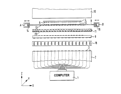
Figures l and 2 show in one rep~esentation two different
embodiments of the printed circuit board testing device
according to the invention, in which the individual elements
are separated from each other in the vertical direction, i.e.
in the direc-ion of the Z-axis of the coordinate system shown,
in order to show the relationships better. It should also be
noted that the elements represent a three-~; m~n -~ional objec L ~
whereby the representation is only in the X-Z plane, i.e. the
plane of the drawing, and the third dimension - the Y
coordinate perpendicular to the plane of the drawing - is nct
shown.
Reference numeral 2 denotes a printed circuit board tester,
which is usually connected to a computer l, with a regular
basic grid ~ o~ contact points to connect the non grid-
orientated test points or connecting points 6 of the test
specimen 4 with the aid of the adapter technique which will be
desc-ibed below. As is usual in the printed circuit board
industry, the connecting points 6 on the wiring plane 4
(printed circuit board, ceramic substrate, etc.) are arranged
in practically any way, i.e. they can for e~ample be arranged
to be partially grid-orientated and/or partially tightly
pac~ed locally, etc. on the printed circuit board 4 to be
tested, and freauently in fact with many hundreds or even
SUB~ ~ JTE SHEET
WO94/11743 2 1 ~ 8 I 0 6 PCT/EP93/01468
-- 7
thousands of test points/connection points 6 per printed
c rcuit board/ wiring plane 4. In order to connect these
irregularly-arranged connection points to the regularly-
arranged contacts of the basic grid 3 of the testing device 2,
a fle~ible adapter foil 8 is provided, which, in accordance
with the usual printed circuit board techniques, has to be
manufactured as an indi~idual printed circuit with contac.
areas or lands 12 and 13 on both sides of the adapter ~oil.
Here the lands 13 facing the testing device 2 are arranged
either e~actly according to the basic grid 3 of the testing
device, or in an intermediate grid which preferably is as
regular as and/or more densely packed than the basic grid 3,
on which a furthe- conversion with known suitable adapter
techniques (adapter plate 9, active basic grid 18) takes
place, whereas the contact areas 12 on the side of the adapter
-oil 8 facing the test specimen are dis.ributed according to
the arrangement of test points or connecting points 6 of the
test specimen 4. In this case each 'and 12 is connec~ed to a
corresponding land 13 on the other side or the adapter foil 8,
i.e. according to usual printed circuit board techniques, with
the aid of printed conductors 16, 17 on one of the t~o
surfaces of the adapter foil, and plated-through holes 19,
shown only in Fig. 5), i.e. conduc~ing areas in the adapter
~oil e2.ending in the direction of the Z-a~is, that is
per?endicular to the adapter foil 8, so that the test current
of the testing device can flow from one contact of the basic
gr-d 3 via the components shown in the drawings, to the
associated contact area 13 on the one side of the adapter foil
and on to the other contac_ area 12 on the otner side of the
adapter foil, and from there to the connecting point 6 of the
test specimen 4 to be tested.
with the aid of frame sections 14, 15 and 19~ at its edges,
the adapter foil 8 can be displaced or elastically elongated
/stretched in the direction ~f its plane by a mechanical
adjustment system A - not shown in detail - in order to adjust
the position of the lands 12 on the side assigned to the test
S~JB~ I I I ~JTE SHEET
21 - 8 - PCT/EP93/01468
specimen 4 as required in relation to the test specimen, whose
position is set by means of a suitable locating hole and an
associated conical pin. Since the test contacts 6 on the ~est
specimen and the corresponding mirror-image lands 12 on the
adapter foil 8 are e~traordinarily small and can therefore
give rise to possible contact faults between the adapter foil
and the test specimen due to manufac'uring length tolerances
between the tes~ specimen and the adapte~roil, the entire
adapter foil can be displaced or elastically stretched within
cer.ain limits in order to achieve the necessary satisfactory
contac- at all contact points. A tensile force can also be
selectively applied to various frame sections 14, 15. Only a
very small amount of displacement and/or stretch in the
adapter foil is usually necessary in order to achieve complete
contact with the printed circuit board to be tested, without
therefore the obviously larger and preferably regularly-
arranged contact areas 13 on the side of the adapter foil 8
faci~g away from the test specimen disengaging from the
associated conductors 20 or test probes 21 of the adapter
arrangement.
In the emboaiment of Figs. 1 and 3, the lands 13 of the
adaster foil 8 are electrically connected via the conductors
20 of a flat contlnuous pressure-transmitting par_ ll of
elastically-compressible, non-conducting elastomer material.
These conduc=ors 20 are then in turn in contact with an
adapter plate 9 which translates the preferably regular
arrangement of conductors 20 or contact areas 13 into the
basic grid of the testing devlce 2 as required, the adapter
plate ~ being connected via a so-called active basic grid 18
to the contacts 3 of the basic grid of the testing device. The
active basic grid is a conventional component which has spring
contacts corresponding to the basic grid of the testing device
2, and provides the necessa~ contact pressure between the
rigid contacts 3 of the testing device and the correspondinglY
arranged contact areas of the adapter plate 9.
SUB~ I 1 1~ JTE SHEET
WO94~11743 2 1 4 81 0 6 PCT/EP93/01468
g
In Fig. 2, a conventional test probe adapter 22 replaces the
conductors 20 in the pressure-transmitting part ll, the
adaDter plate 9 and if necessary the active basic grid 18,
inasmuch as it involves spring test probes. In this
embodiment, the elastically-compressible pressure-transmitting
part ll (e.g. made of rubber) has holes or channels
corresponding to the arrangement of adapter foil lands 13 and
the test probes pass through these holes or channels in the
pressure-transmitting par. ll and make contact with the lands
13. ~ere the entire area of the pressure-transmitting part ll
is pressed by the uppermost test probe guide plate of the
conventional test probe adapter 22 in the direction o, the
adapter foil 8, thus producing the necessary elastic pressure
.orce over the entire area of the adapter foil 8. In this case
the test probe adapter connects in the known manner the
contact areas 13 to the contacts 3 of the testing device and
in this way translates - where necessary - from a closely-
spaced grid in the adapter foil 8 to the basic grid of the
testing device. It is perfectly possible to use a so-called
~ull-grid test probe adapter, i.e. a test probe adapter in
which all grid points are occupied by a test pro~e, even ir
not all of them re connected to the test specimen via the
adapter foil, which gives the advantage that in spite of
di~ erent adapter foils and test specimens, the same test
probe adapter can be used. E~amples of conventional test probe
adapters are described and claimed in the applicant's
EP 26 824 Bl, EP 315 707 Bl or EP 215 146, but these are
alwavs represented as spec~al/individual adapters and not as
full-grid test probe adapters.
The pressure-transmitting part ll is preferably a rubber mat
of sandwich construction, whereby the part lying against the
adapter foil 8 is of compressi~le rubber and the part facing
the printed circuit ~oard testing device consists of a
~;m~n~ionally-stable epoxy resin, ~or example, so that the
pressure-transmitting part ll is by and large compressible on
one side in the vertical direction, i.e. in the direc_ion cf
SUBS ~ ITE SHEET
WO94/11743 PCT/EP93/01~8
2~ 48106 '~
-- 10 --
the Z-a~is, but is dimensionally-stable in the X-Y plane. Such
a pressure-transmitting part 11 of the embodim.ent of Figure 2
can be provided with holes/channels of 10 to 0.5 mm diameter
- and less, i~ such a way that a sandwich arrangement of epo~
resin plate/rubber mat/epoxy resin plate is~drilled in the
clamped state, after which the top epoxy rë~in plate, which is
merely required for the drilling operation, is removed and is
not thererore glued to the rubber mat like the bottom epoxy
resin plate.
In the embodiment in Figure 1, the pressure-transmitting par~
11 has conductors 20 arranged in the grid pattern of the
contacts 13 and these are incorporated in the rubber mat
and/or the sandwich construction of epog~ resin plate and
rubber mat glued to it. As a-result, these conductors 20
e~tend .rom the top face to the bottom face of this sandwich
construction and form lands or contact areas arranged in the
grid on the top and bottom faces. Here these conductors 20,
which are preferably wires of 0.2 to 0.4 mm diameter, for
e3ample, are arranged obliquely to the plane of this pressure-
transmitting par~. This produces a spring compliance in the
lands formed by them on the top and bottom faces in the
direction of the Z-axis, i.e. the inclination of these
conduc.ors or wires 20 in the pressure-transmitting element 11
provides an electrically-conducting component at specific grid
points in the vertical direction of the pressure-transmitting
element 11, which does not have the drawbacks of the
conventional vertica~ conducti~g plates, whlch have verv thin
and very closely-spaced, fine gold wires extending
perpendicularly to the plane of the plate, and whose spring
compliance is merely due to their bending stress.
The conventional test probe adapter 22 shown in Fig. 2 is one
such as is more precisely described in the above-mentioned
EP 315 707 Bl, for instance. But the other conventional test
probe adapters can be used. It is essential that the entire
area or the uppermost test probe guiae plate of the test probe
SUB~ I I I ~TE SHEET
WO94/11743 21~ 810 6 PCT/EP93/01468
adapter 22 in Fig. 2 makes contact with the lower side of the
pressure-transmitting element ll in Fig. 2 in.o~der to achieve
continuous, l~in~r support of the flexible foil 8 in this
way.
In a concrete, preferred embodiment of a printed circuit board
of the type described and discussed here, the adapter foil 8
consists of a polyimide material or (not quite so
advantageous) an epogy resin material, and the foils can have
a thickness of 0.025 mm or 0.050 mm. Since the test contacts 6
of the printed circuit board 4 to be tested can have a width
down to O.l mm, with a ce~tre-to-centre distance down to
O.1 mm and less, the cor-espondingly arranged and formed lands
12 on the adapter foil 8 have a width or a diameter of
aporo~imately 0.015 to 0.020 mm, whereby copper with
preferably a gold coating is used as the contact material. The
lands 13 on the opposite side of the adapter ~oil have
diameters down to about 0.6 mm, and the horizontal
displacement or elongation of the adapter foil 8 is typically
only 0.2 mm over an overall length of appro~imately 300 to
500 mm. As a result, any spontaneous deviations in the
position of the test contacts 6 or the lands 12 from the
reference position, which occur during the manufacture of the
printed circuit boards to be tested, or during the manufacture
of the adapter foil, can then be compensated very
satisfactorily.
The pressure-transmitting par~. ll in the embo~iment of Fig. 1
consists, in a preferred em~o~;ment, of a rubber mat of
appro~imately 2 to 5 mm thickness, which can for e~ample be
glued to a thi~ epozy resin plate in order to obtain
reasonable stability in the X-Y plane. The conductors 20 in
the form of wires are, for e~ample, arranged in a 1.27 mm grid
and have a typical thicXness of 0.2 to 0.4 mm. These wires can
be gold-plated or even gold.
SUB~ I I I ~TE SHEET