Note: Descriptions are shown in the official language in which they were submitted.
- ~ w~ s~toss~3 2 1 4 8 1 2 ~ PCl'lUS94109444
ANTENNA ARRANGEMENT FOR A
WII~ELESS CO~MUNICATION DEVICE
Field o~ the Invention ~ -
The present invention relates generally to antenna arrangements
and more particularly to an antenna arrangement for a wireless
communication device.
Backgrolmd of the Invention
Wireless communication devices in many forms are becoming
increasingly popular. The term "wireless communic~tion device" in this
~15 context encompasses cellular telephones, patio telephones, cordless l;
;; telephones in their many differell~ forms, personal commurlication
" devices, and the like. Wireless communication devices are characterized -
by being easily transportable by the user.
Typically, w~reless communication devices include an antenna ~-~
~ a~rangement for providing the wireless commur~cation. The antenna -~
arrangement may pronde, in cooperation with: circuitry of the wireless
communication device, transmit, receive or t}anscéiviIlg functions for the
wir~less commuI~ication device. Desirable antenna ~rrangements are
small, reliable and~manufactur~ble. Since the wireless communication
~device is indeed ~ansportable, desirable antenna arr~ngements are also
typically moveable between a stowed and an unstowed posi~on, for
exam~le,la retracted and an extended p~sition, respecti~7ely. I
Designers of antenna arrangements strive to op~nize the size,
r eliability and ~manufacturability of the antenna arrangement while
~ achieving desirable performance for the antenna arran8ement. Since
technology is driving the si~e of wireless cornmunication devices to be -~
smaller, the antenna arrangement for those smaller devices must also be
made smaller to preserve the anténna arrangement's stowable feature and
desirable performance. FIGs. 1-3 illustrate first, second and third antenna
~ :
~: :
~ .
wo 95/()8853 1 ?~ 5 pcTruss~ms
arrangements for a wireless communication device which seek to
op~mize both size and performance of the antenna arrangement in
accordance with the prior art.
FIG. 1 illustrates the first antenna arrangement 102 for a wireless
communication device 100 in accordance with the prior art. A detailed
description of the antenna arrangement 102 in FIG. 1 is given in U.S.
Patent 4,121,218. The antenna arrangement 102 of FI~. 1 generally
includes a helical antenna 104 and an extendible haif-wave antenna 106.
The helical antenna is coupled to circui~y 108 of t~e wireless
communication device 100. The extendib~e half-wave antenna 106 is
adapted to be capacitively coupled to the helical antenna 104 when in the
extended position and to be substantially decoupled therefrom when in a ~-
retracted position (shown in dotted lines). Ad~antages of the antenna
arrangement 102 include contactless coupling between the helical antenna -
104 and the extendible half-wave antenna 106 and the performance of the
antenn~ arran~ement as indicated by the height 112 where the current
maximum of the extendible half-wave antenna 106 occurs when the
extendi~le half-wave antenna 106 is extended. However, a disadvantage of
the antenna arrangement 102 is that its overall physical height 110 is too
long to meet present day needs of miniature wireless communication
devices.
FIG. 2 illustrates a second antenna arrangement 202 for a ~
communication device 200 in accordance with the prior art. A detailed --
descr~ption of ~he antenna arrangement 202 in FIG. 2 is given in U.S.
2s Patent 4,86~s,576. I~e antenna arrangement 202 includes a helical antenna204 coupled to circuitry 208 and an extendible half-wave hel;cal antenna
206. An advantage of the antenna arrangement 202 over the antenna ~-
arrangement 102 of FIG. 1 is that the height 210 is lower than the height
110 of ~e an~e~na arra~gement 102. However, a.disadvantage of the
antenna arrangement 202 is that the height 212 where the current
maximum of the extendible half-wave antenna 206 occurs when the
extendible half-wave antenna 206 is extended, is lower than the height 112
w~ere the current maximum occurs in FIG. 1. Therefore, ~e performance
of the antenna arrangement 202 was sacrificed for a shorter antenna.
3~ FIG. 3 illustrates the ~ird antenna arrangernent 302 for a wireless
cornmur~ication device 300 in accordance with the prior art. The antenna
~) wo gs/08853 21 ~ 812 S PCT/US94/()9~4~
arrangement 302 generally includes a ~irst straight portion 304 and a
second helical portion 306 which is electrically isolated from the first
straight portion 304. The straight por~on and the helical portion 306 each
have an electrical wavelength of 1/4 wavelength. The straight portion
304 includes a term~nal 310 for connec~on to a connector 312 when the
antenna arrangement is extended. Likewise, the helical portion 306
includes a terminal 314 for connection to the connector 312 when the
antenna arrangernent is retracted. Circuitry 308 is coupled to the antenna
arrangement 302 via a connector 312. An advantage of the antenna
arrangement 302 is that its height 316 is reduced even further than that ~-
represented in FIGS. 1 or 2. However, a disadvantage of the antenna
arrangement 302 is that the height where the current maximum occurs -~
when the antenna arrangement 302 is extended is much lower (shown
below the housing of the device) than the height of the current~ maximum
as shown in FIG5. 1 or 2. A further disadvantage is that metallic contacts
of the connector produces electrical noise which reduces reliability.
Therefore, there is a need for an antenna arrangement for a wireless
communication device having further reduced dimensions while ~-
, . .
achie~ring desirable performance as well as maintaimng acceptable
reliability and manufacturability. -
Brief Descnption of the Drawings
~.
FIG. 1 illustrates a first antenna arrangement for a wireless
communication device in accorclance with the prior art;
FIG. 2 illustrates a second anterma arrangement for a wireless
cornmunication device in accordance with the prior art;
~IG. 3 illustrates a third antenna arrangement for a wireless
;commlumcahon ~evice in accordance with the prior art,
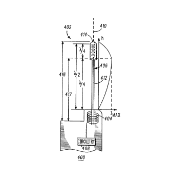
FIG. 4 illustrates an antenna arrangement for a wireless ~;
~; commurLica~on device, wherein a por'don of the antenna arrangement is
' ~ extended beyond the wireless commur~ication device, in accordance with
the present invention;
' FIG. 5 illustrates an antenna arrangement for a wireless
33 communication devlce, wherein a portion of the antenna arrangement is
:
- 3-
:
wo gs/08853 2 ~ 4 8 12 5 PCT~lJS94/0944~ ~
stowed within the commumcation device, in accordance with the present
invention; and
FIG. 6 illustrates a schema'dc diagram for the antenna arrangement
of FIGs. 5 and 6 in accordance with the present invention.
. .
Detailed Description of aP~ef~ dEmbodiment
FIG. 4 illustrates an antenna arrangernent ~2 for a wireless
communication device 400, wherein a moveable element 406 of the
antenna arrangement 4û2 is extended beyond the wireless communication
device 40û, in accordance with the present invention. The wireless -~-
communication device 400 generally includes the antenna arrangement
402 and c~rcuitry 408 coupled to the antenna arrangement 402. The
antenna arrangement 402 generally includes a first element 404 and a
second element 406.
. ~ ,,
The first element 4û4 is coupled to ~e circuitry 408 of the wireless
communication device. The second element 406 is movable between a
first position (shown in FIG. 4) and a second position (sho~n in FIG. 5)
relaffve to the first element 404. Ihe performance of the antenna
~o arrangement 4û2 is substan~ally less desirab}e when the second element
406 is between the first and the second position than the performance of
the antenna arrangement 402 when the second element 406 is at either the
first or the second position. The second element 406 is mechanically -
spaced apart from and substantially elec~ical}y coup}ed to the first element
404 in bo~ the first and the second positions.
Since the second element is mechanically spaced apart from and - -
substantia}ly electrically coupled to the first element in both the first and -
the second position, the antenna arrangement of the present invention
optimizes both! size andi p~rforrnance in such a way that was not achieved
in the prior art as shown in FIGs. 1-3. A detailed description of such -
optimization is given below. -~-
In accordance with a preferred embo~iment of the present
invention, t~e second element 406 is movable along a longitudinal axis
410 of the second element 406. ~xial movement of the second element
3~ 406 is advantageous for easily stowing the second element 406 within the
communication device 400. However, other antenna arrangements may
:~ ' -
~: :
l ~ - 4 -
~ wo 95l08853 2 1 4 8 1 2 5 PC~IUS94/()9444
be implemented to move in other axes such as rotational or lateral, while
obtaining the same advantages of the present invention.
In the preferred embodimeIlt of the present invention, the second
element 406 is substantially extended beyond the w~reless communicatior
device 400 in the first position (see FIG. 4) and is substan~ally stowed ~- -
within the wireless communication device 40û in the second position (see
FIG. 5~. AlternativeIy, the second element 406 may be stowed outside the
wireless commw~ication device 400. Further, the second element 406 may
itself be a telescoping element and remain within the scope of the present
0 invention.
In the preferred embodiment of the present invention, the second
element 406 comprises a first portion 412 having a straight form and a ;
second portion 414 having a helical form, wherein the first portion 412 is
electrically coupled to the second portion 414. In the preferred
embodiment, the coupling between the first portion 412 and the second
portion 414 is a direct connection made by forming ~e first portion and
th~ second portion 414 from a single piece of wire. How~ver, the fi~st
portion 412 and the second port;on 414 may alternatively be cons~ucted of
two separate wires and thereafter electrically and mechanically connected, ;
such as with solder or a weld joint.
The antenna arrangement 402 of the present invention as shown in
FIG. 4 is similar to the antenna arrangement 302 of the prior art as shown
in FIG. 3 in that the moveable portion of the antenna arrangement 402 of ~;
the present inven~ion includes both a straight form and a helical form.
The difference between the present invention and the prior art is that in
the present invention the first portion having a straight form 412 is
electrically coupled to the second portion 414 having a helical form;
whereas, in the pr~or art the portion 304 having a straight form is
elèc~Ically isolat~d from'the second portion 306 having a helical form.
The advantages of electrically coupling the first portion 406 having the
straight form and the second portion 414 having the helica} form in the
~ present invention will be described further below.
Alternatively, the first portion 412 having a straight form of the
second element 406 may instead have a helical form with a helical
3~ ~ diameter smaller than the helical diameter of the second portion 414
having a helical ~orm. A first portion 412 having a helical form provides
::
.
wo ss/osss3 214 ~12 5 pcTrt~s9~lo9~
the advantage of even further reducing the height of the second element
406. However, mechan~cal reliability of the second element 406 is
sacrificed because a helical coil has less memory against permanent
mechanical deformation than a straight form. ~
In the preferred embodiment of the present invention, the first
portion 412 having a straight form is coupled to the first element 404
when the second element 406 is moved to the ~irst position (see FIG. 4)
and the second portion 414 having a helical form is coupled to the first
element 404 when the second element 406 is moved to the second position ;~
0 (see FIG. 5). ~
In the preferred embodiment of the present invention, the antenna -
arrangement 402 operates over a frequency band. The ffrst portion 412 and
the second portion 414 toge~er comprise an effechve electrical length ~;
defined by an integer multiple of one half wavelength at at least one
frequerlcy in the fre~uency band. As shown in FIG. 4, the second element ~ ~
406 has an e~ectAcal length of one half wavelength, wherein the ~irst ~ -
portion 412 having the straight form has an electrical length of one~
quarter wavelength and the effective electrical length of the second
pornon 414 h~ving a heIical form is also one quarter wavelength.
In the preferred embodiment, the height 417 where the maximum
current occurs is at the junc'tion of the first portion 412 and the second
. . .
portion 414. ~Forming the second element 406 in this way provides a
reduced antenna height 416 while providing a maximum current height
417 ~ear the top of the second element 406. The present invention
2~ advantageously provides the height 417 where the maximum current
occurs in the present invention arL the same height 112 as shown in FIG. 1
of the pri~r art, while substantially reducing the height 416 of the ~-
extendible element 406 in the present invention as compared to the height
110 of the exten~dible element 106 in the prior art;~ When comparihg the
present invention as shown in FIG. 4 to the prior art in FIGs. 2 and 3, the
.
structure of the second element 406 of the present invention provides the
same or less height 416 whi1e~achieving a greater height 417 at the point
where the current maximum o~curs.
In the preferred embodiment of the present invention, ~e first
3~ element 404 has a helical element. The first element 404 generally
represents an impedance transformer for transforming the impedance of
:
- 6 -
'! wo 95/08853 2 1 ~ ~ 1 2 ~ PCT/llS9~/094~-1
the circuitry 408 to the driving point impedance of the second element 406
to produce an impedance rnatch. The first element 404 provides
connectorless intercoupling similar to that shown in FIGs. 1 and 2 of the
prior art but different from the connector arrangement shown in FIG. 3. A
contactless, connectorless arrangement of the present invention is an
improvement over the connector ~y~Lell~ of the prior art as shown in FIG. -
3 in that the problems of contaminated and wearable contacts are
eliminated.
ln the preferred embodiment of the present invention, the first
0 element 404 comprises an electrical length defined by an odd integer
multiple of one quarter waveleng~h a~ at least one frequency substantially
near the frequency band. In particular, the elec~rical length is one quarter
wa~elength.
FIG. 5 illustrates an antenna arrangement 402 for a wireless
cornmunication device 400, wherein a portion 406 of the antenna
arrangement 402 is stowed within the wireless communication device 400,
in accordance with the present invention.
In the preferred embodiment of the present invention, the first
element 404 is wound in a first direction (as indicated by arrows 405 on the
helix3 relative to a forming direction 501 and the helical form vf the
second por~on 414 of the second element 406 is wound in a second
direction (as indicated by arrows 415 on the helix), opposite to the first
direction, relative to the forming direction 501. The helical forms are
wound in opposite directions in order to reduce coupling between the first
2s element 404 and the second portion 414 of the second clement 406.
Reduced coupling is necessary to achieve a desirable impedance match
given the physical dimensions of the antenna arrangement 402 of the
present invention. However, other antenna arrangements may utilize
helic~l for~s w~und in the same direction given other dimensioAa
requirements and fall within the scope of the present invention.
f Coupling energy between the first element 404 and the first 412 or
second 414 portion of the second element 406 in this manner is known a~ -
mutual coupling. Mutual capacitive coupling is described in detail in V~S.
Patent No. 4,121,218, herein incorporated by reference. Mutual coupling
3~ includes both capacitive coupling and inductive coupling. When the
helical forms are wound in the same direc~on the capacitive coupling is
~: .
wo ss/088s3 21 4 8 i 2 5 PCT/US94/~g44 1 --~
added to the inductive coupling to produce a total mutual coupling greater
than either the capacitive coupling or the inductive coupling. When the
helical forms are wound in opposite directions, the inductive coupling is
subt~acted from the capacitive coupling to produce the total mutual
coupling that is less than the capacitive coupling and therefor less than the
total mutual coupling when the helical forms are~;~7ound in the same
direction.
Since the second portion 414 of the seco~l element 406 is
substantially electrically coupled to the first element 4Q4 in the second
position, both the second por'aon 414 and the first element 404 together
form the radiating portion of the antenna arrangement 402 when the
second element 406 is at the second position. An advantage of such a
structure is that the height 503 of the first element 404 is reduced relative - -
to the prior art shown in FIGs. 1 and 2 without sacrificing performance of
the antenna arrangement 402 when the ~econd element 406 is at the
second position. Reduced heigh~ 503 of the first element 40~ is important
- for ~he aesthehc appearance of small wireless communication devices.
To provide proper performance, the antenna provides an input
impedance which is similar in both the first position and the second - -
position. This is achieved through proper selection of the dimensions of
the straight portion 412 and the helix portion 414.
ln accordance with the ~refe~l~ed embodiment of the present
invention, the first portion 412 forms a first component of a transmission
line 505 and the second portion 404 forms a radiating element o~ the
2~ antenna arrangement 402 when the second element is at the second
position. A second component of the transmi~sion line 505 in~ludes a
conductive por~on 507 and a dielectric portion 509. The dielectric portion
5Q9 is disposed between the first component 412 of the transmission line
~505 and 'the cdnductive portion 507. In the preferred embodiment, the
transmission line 505 is formed as a coaxial trar ~mi~sion line; however, '
other transmission line structures such as strip line, microstrip and
balanced transmission line structures may also be implemeIlted in
.
accordance with the present invention. In the preferred embodiment, the
conduc~ve portion 507 is a metal tube; however, the conductive portion
3~ 507 may also comprise a conductive surface inside the housing of the
wireless eommun~ca~on device 400.
~ .
~) wo ss/osss3 214 812 5 PCTtUS9~/09441
The transm~ssion line 505 has an electrical length at least partiall~
relat~d to an electrical characteristic, for example perrnitivity, of the
dielectric portion 509 as well as the electrical length of the conductive
portion 507. These characteristics may be adjusted to achieve a desirable
impedance match for the antenna arrangement 402 according to
dimensional requirements.
In accordance with the preferred embodiment of the present
invention, the transmission line 505 comprises a reactive termina~on. In
the preferred embodi~ent, the reactive term~nation is an open circuit, '';
0 however a short circuit or lumped element may also be implemented in
accordance with the present invention. The impedance at the junction of : -
the straight portion 412 and the helix portion 414 in relation to the
conductive tube 507 is made to be low so that a current maximum occurs. .
Multiple configurations of reactive terminations and lengths of the
s~aight section 412 and tube 507 will achieve this condition. The final
configurations for 412, 507 and 509 are selected from the allowed
parameters in both the first and the second position.
FlG. 6 illustrates a schematic diagram for the antenna arrangement
402 of FIGs. 5 and 6 in accordance with the present invention. The
schematic representation of the first element 404 and the schematic
representation of the second element 406 each contain a representation of
inductance, capac~tance and resistance in ~ose elements as is well known
in the art. A capacitor 601 represents the capacitive coupling con~ibution
to the total mutual coupling. The bi-d~rectional arrow, represented by
reference numeral 603 between each elemen~, represents the inductive
coupling contribution of the total mutual coupling of the antenna
arrangement. Dots 605 and 607 together represent the phase of the
magnetic coupling between the first element 404 and the second element
406. Capad~ve !couplingl occurs between the unconnected ends of the!~
helixes 404 and 414 in the first position and between the open end of the ;
helix 404 and the open ~nd of the straight portion 412 in the second
position. It is maximized by the high voltages which exist on these
locahons during operation. Inductive coupling occurs between the
connected ends of the helixes 404 and 414 in the second position. The ~;
- 3~ inductive coupling is maximized by the high current existing at these
locations during operation.
-
- 9 -
, -
WO gS/138853 214 812 S PCT/US94/Og44~
The present inven~on is primanly intended to be used for antenna ;
arrangements operating in the range of 150 - 900 MHz, and in the preferred
embodiment, 900 MHz. The following description provides a detailed
descrip~ion, by example, of t~e antenna arrangemént 402 in accordance
;, with the present invention. The preferred e~bodiment has a helix 404
with a diameter of 7.0 mm and a length of 9.0 mm with 4 turns. The helix
414 has a length of 33.3 mm and a diametèr of 4 6 mm with 10.75 turns.
The straight portion has a length of 64 mm. The dielectric in the tube is
Teflon with a dielectric constant of 2.1.
~ ''''''
',~
,
:
:
-
, ,
- ;-
~: :
,
.
~ .~
: ~ : . ..
~ , - 1 0 -