Note: Descriptions are shown in the official language in which they were submitted.
2148187
SYSTEM FOR CONTROLLING THE EFFECTS
OF NOISE IN TELEVISION RECEIVERS
FIELD OF THE INVENTION
0 The present invention relates in general to
television receiver circuitry. More particularly, it
relates to circuits and methods for controlling the
effects of various types of noise signals that may be
experienced during analog television reception.
BACKGROUND OF THE INVENTION
3 Television receivers are vulnerable to noise
signals from various sources. The interference usually
results from electromagnetic radiation which interferes
with the broadcast RF signal. Typical sources of such
interference are automotive ignition systems and
household motors such as washing machines, dryers and
refrigerators. Similar types of interference may also
be caused in a broadcast RF signal by high definition
television systems and digitized 525 line systems. The
interfering signals often appear as bright or dark
spots on the television screen.
The patent literature describes numerous
approaches to reducing or eliminating the problems
caused by interference in broadcast television and/or
video signals. The general approach to the problem has
been to design circuits that combat the effects of
interfering signals, and then place these circuits in
the signal path of the incoming television/video
- 1 -
214x187
- 2 -
signal. Unfortunately, few circuit designs deal
effectively with more than one type of interference.
Accordingly, if it is desired to combat f our types of
interference, the television receiver will typically
have four interference compensation circuits placed in
its incoming signal path. Each of the four circuits
process the incoming signal regardless of whether
interference is present, and regardless of whether the
interference is the type that the particular circuit is
designed to respond to. Also, such schemes may
actually cause interference because a given circuit
could react unpredictably when exposed to a type of
interference that it was not designed to combat, or
when trying to correct problems that have already been
acted on by another circuit.
Because television pictures are forn~ed by
scanning an image and partitioning that image into a
plurality of horizontal lines, the signal information
from image line to image line is highly redundant for a
significant percentage of images. The horizontal lines
are sequentially transmitted to the television's
receiver circuitry where they are reconstructed, line
by line, into the original image and shown on the
television screen.'
U.S. Patent. No. 2,996,576, issued to Do_ lbv,
discloses a system which takes advantage of the line to
line signal redundancy inherent in scanning and
partitioning images, and minimizes the effect of
television signal disturbances in video
recording/reproducing systems such as video recorders
and video disk systems. Video signals are typically
recorded as a frequency modulation (FM) of a carrier.
The Dolby system responds to disturbing signals that
have sufficient amplitude to cause loss of the FM
carrier. Thus, video signal loss may be detected by
detecting the loss of the FM carrier. This is commonly
- 2 -
2148187
- 3 -
referred to as "envelope detection." Upon detection of
a video signal loss, the signal for the preceding image
line, which is delayed by one image line period, is
substituted for the lost signal to minimize picture
disturbance.
The relatively large number of defects in
video recording media makes it imperative to include
signal compensation systems in video
recording/reproducing apparatus. U.S. Patent
No. 5,032,915, issued to Ichimura, discloses such a
noise detection and dropout sensing and compensation
circuit for use in video recorders.
By contrast, it was, for a period of time,
too costly to include such interference correction
systems in consumer television receivers. however,
with the incorporation of charge transfer device delay
lines in television receivers to perform comb filtering
of the luminance signal, it has become practical in
i consumer televisions to consider correcting
interference signals such as, for example, impulse
noise. The interference correction can be performed by
video signal substitution as in video
recording/reproducing systems. f~owever, the detection
of noise or defects in broadcast television signals
presents different problems than those encountered in
video recording/reproducing systems.
One such difference occurs where the
interference or noise creating the picture disturbance
does not have sufficient amplitude, as would an
impulse-type noise, to eliminate tire broadcast signal
carrier. In those cases, one cannot rely upon envelope
detection of the broadcast signal carrier to determine
when defects are present in the signal. In addition,
television signals are broadcast as an amplitude
modulated carrier so that amplitude changes are
generally not indicative of the presence of noise or_
- 3 -
. ~ 2148187
- 4 -
signal defects. In other words, because the dynamic
amplitude range of the baseband video signal is very
large, noise can have amplitudes ranging from barely
perceptible to large enough to overload the receiver
circuit.
U.S. Patent No. 4,353,093, issued to Durbin,
recognized that impulse noise, i.e., a noise signal
that may supersede the video signal on all or a part of
an image line, typically has a broad energy spectrum
and causes interference across many television
channels. Therefore, energy from the impulse is likely
to be included in the sound component of a particular
television signal even though the sound component is
broadcast on a carrier separate from the video signal
component of the particular television signal. Because
the sound component is a high frequency modulated wave
form in the baseband TV signal amplitude detection of such
a signal
can be used for effectively detecting the presence of relatively
small values of narrow duraLion/wider bandwidth noise.
In the Durbin patent, a phase-locked loop
(PLL) synchronous detector arrangement is responsive to
a bandpass filtered version of the modulated sound
carrier for detecting amplitude variations of the sound
carrier. Compensation circuitry, including a delay
line, coupled to the output of the synchronous detector
substitutes a prior image line for the present image
line in response to the level of the detected amplitude
variations. In addition to this PLL synchronous
detector arrangement for detecting impulse noise,
conventional intercarrier detection circuitry is
required for detecting the audio and video information
from the composite television signal.
U.S. Patent No. 4,514,763, issued to Rindal,
takes the same basic approach as the Durbin patent to
eliminating impulse noise. The Rindal patent, however,
uses a PLL for detecting the audio information and
- 4 -
X148187
- 5 -
providing a defect control signal for reducing impulse
noise. One drawback of using audio high frequencies
(which are not in the video channel) is that the sound
channel could be affected when the video is not, or
vice versa. Thus, the reliability of such systems is
compromised.
Thus, currently available television signal
noise reduction systems do not provide the user with
sufficient control over how and when the individual
noise reduction circuits are used. Accordingly, the
available systems do not counteract the potentially
unpredictable reaction of a noise reduction circuit
when it receives a type of noise or other signals that
it was not designed to process. Also, the individual
circuits available for combating interfering signals
such as impulse noise, for example, do not provide
sufficient reliability.
. SUNJMARY OF THE INVENTION
Thus, it is an object of the present
invention to provide a circuit and method for
organizing and controlling the individual interference
compensation circuits that comprise a television noise
reduction control system.
It is another object of the present invention
to provide a television noise reduction control system
which allows the user to control how and when
individual interference compensation circuits in the
system are used.
It is another object of the present invention
to provide a television noise reduction control system
in which a particular interference compensation circuit
in the system is activated only when needed.
It is another object of the present invention
to eliminate the potentially unpredictable reaction of
a television interference compensation circuit when it
- S -
214818
-
receives a type of noise or other signals that it was
not designed to process.
. It is another object of the present invention
to provide more reliable individual television
interference compensation circuits for use alone or in
a television noise reduction control system.
These and other objects are realized in
accordance with the present invention by providing a
circuit and method for controlling the effects of noise
signals received by a television receiver. The circuit
includes an on-screen disturbance control menu system.
Each on-screen menu option enables an individual
circuit designed to reduce the effects of a particular
types of noise in the composite video picture signal,
including compensation circuitry for reducing the
effects of impulse noise signals, longer-duration noise
signals, and CW noise signals. The interference
compensation circuits are arranged in a cascade manner,
a' and may operate alone or in combination.
The on-screen disturbance control menu system
of the present invention is controlled by a
microcomputer/processor (MPU). The on-screen menu
system is totally under user control, allowing the user
to ameliorate the effects of impulse noise
disturbances, longer duration disturbances and/or CW
disturbances without requiring the user to understand
the nature of these disturbances. The user simply
chooses the method that works the best. Alternatively,
the MPU may be programmed to automatically scan through
the compensation circuit options, and the user can stop
the scan once it reaches a circuit that solves the
problem. Also, the MPU may be programmed to
automatically scan through the compensation circuit
options, and then automatically choose the compensation
circuit that reacts to and solves the problem. Also,
the MPU could be programmed to automatically enable the
- 6 -
2148187
appropriate compensation circuit when a detection
circuit detects a particular type of interference.
Another aspect of the present invention is a
circuit for processing a composite video signal and a
high frequency luminance signal. The high frequency
luminance signal is produced by a comb filter that
separates the chrominance and luminance signals. The
processing circuitry detects the composite video signal
and the high frequency luminance signal, and enables
compensation circuitry for reducing the effects of
impulse noise in the composite video signal depending
on an assessment of both signals. The detection
circuitry includes a comparator for sensing when the
amplitude of the composite video signal exceeds a first
predetermined value, a second comparator for sensing
when the amplitude of the composite video signal is
less than a second predetermined value, and a third
comparator for sensing when the high frequency
luminance signal exceeds a third predetermined value.
The output of the detection circuitry is used to
produce a control signal to enable a tracking and hold
circuit, which holds the video signal level at the
level of the video signal received just prior to
activation of the tracking and hold circuit.
The above-described circuit uses high
frequency video together with the composite video
signal in order to flag the presence of an impulse.
This improved method of detecting the impulse is not
just level-dependent, but also uses detection of high
frequency energy. If both the level dependent and high
frequency energy detection circuits indicate the need,
the tracking and hold circuitry will hold the picture
signal at the level that occurred just previous to the
disturbance to minimize picture distortion.
Accordingly, the present invention achieves
several advantages. In particular, the circuit and
2148187
_8_
method of the present invention provides apparatus and
method for organizing and controlling the individual
circuits that comprise a television noise reduction
control system. The invention further provides a
television noise reduction control system which allows
the user to control how and when individual noise
reduction circuits 3.n the system are used. The present
invention also reduces the potentially unpredictable
reactions of a noise reduction circuit when it receives
a type of noise or other signals that it was not
designed to process. This is accomplished by allowing
the user to activate an individual noise reduction
circuit in the system only when it is needed. Finally,
the inventions provide reliable individual television
noise reduction circuits which can be used alone or in
a television noise reduction control system.
BRIEF DESCRIPTION OF THE DRAWINGS
'' FIG. 1 is a block diagram of a television
noise reduction control system embodying the present
invention;
FIG. 2 is a block diagram of a television
receiver circuitry embodying another preferred
embodiment of the present invention;
FIG. 3 illustrates a traditional mathematical
representation of a system impulse response in the time
and frequency domains;
FIG. 4 illustrates the bandpass and baseband
selectivity of a typical television receiver;
FIG. 5 illustrates an impulse signal that
exceeds the boundaries of a valid signal range;
FIG. 6 illustrates the typical configuration
of a tracking and ho7_d circuit suitable for use in
connection with the present invention;
FIG. 7 illustrates one example of a notch
filter made from a bandpass filter;
- 8 -
2148187
- 9 -
FIG. 8 illustrates a voltage variable notch
filter for tracking a CW or carrier input signal;
FIG. 9 illustrates an example of a voltage
variable notch filter circuit; and
FIG. 10 illustrates an alternative approach
to designing a circuit to eliminate CW disturbances by
using a bandpass filter whose center frequency is
proportional to the clock signal that is being
developed from a tracking filter.
DETAILED DESCRIPTION OF THE
PRESENTLY PREFERRED EMBODIMENTS
Prior to the present invention, the general
approach to compensating for picture distortion caused
by interference signals in broadcast television and/or
video signals has been to permanently place the desired
interference compensation circuits in the signal path
of the incoming television/video signal. While there
are some circuits which allow a user to deal with one
type of noise, such as gaussian noise, few circuit
designs deal effectively with more than one type of
interference. Accordingly, a television receiver that
is designed to combat four types of interference will
typically need to have four interference compensation
. 25 circuits permanently placed in the incoming signal
path. Each of the four circuits processes the incoming
signal regardless of whether_ interference is present,
and regardless of whether the interference present is
the type that the particular circuit is designed to
respond to. Also, such schemes may ac~ually cause
picture distortion because a given circuit could react
unpredictably when exposed to a type of interf-_erence
that it was not designed to combat, or when trying to
correct problems that have already been acted on by
another circuit.
g _
2148187
- 10 -
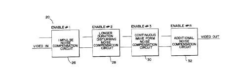
FIG. 1 is a block diagram of a television
noise reduction control system 20 which embodies the
present invention and solves the problems described
above. The illustrated embodiment is a circuit and
method of selectively enabling one or more desired
interference compensation circuits via an MPU
controller 24, shown in FIG. 2. The MPU 24 may be the
same MPU that controls the tuning and other control
functions of a conventional consumer television
receiver.
The MPU 24 is programmed to enable or disable
a variety of interference compensation circuits as
instructed by the user. The user provides instructions
to the MPU 24 through an on-screen menu, allowing the
user to enable or disable a series of compensation
circuits by pushing the designated buttons on the
television receiver or a remote control. FIG. 1
illustrates three specific types of compensation
circuits--an impulse noise compensation circuit 26, a
longer duration noise compensation circuit 28, and a CW
noise compensation circuit 30. FIG. 1 also illustrates
that any number of additional noise compensation
circuits 32 could be added to the system 20. When a
compensation circuit is enab7_ed by the user, it
receives the incoming television/video signal and acts
on the particular type of interference that the
compensation circuit was designed to combat. When a
compensation circuit is disabled by the user, the
compensation circuit passes the television/video signal
without significant modification.
'the on-screen control menu offers options
which correspond to the compensation circuits
illustrated in FIG. 1. For example, setting A on the
on-screen menu could correspond to the impulse noise
compensation circuit 26, setting B to the longer-
duration noise compensation circuit 28, and setting C
- 10 -
,.. , ~, _.
2148187
- 11 -
to the CW noise compensation circuit 30. The
compensation circuits are arranged in a cascade manner,
and may be enabled by the MPU 24 to operate alone or in
combination.
An important feature of the present invention
is that the user is not required to understand and
recognize the type of interference being experienced in
order to use the system 20. The circuits are easily
enabled and disabled by the user through the on-screen
menu and the MPU 24, allowing the user to simply cycle
through the circuit options and choose the appropriate
option. Alternatively, the MPU 24 may be programmed to
automatically scan through the compensation circuit
options, allowing the user to stop the scan once it
reaches a circuit that solves the problem. Also, the
MPU 24 may be programmed to both automatically scan and
choose the appropriate compensation circuit option to
solve an interference problem. Also, the MPU 24 could
' be programmed to automatically enable the appropriate
compensation circuit when a detection circuit, such as
the longer duration disturbance signal detection
circuit 73 or the CW detection circuit 77 shown in FIG.
2, detects a particular type of interference.
The system 20 illustrated in FIG. 1 may be
used with any type or number of compensation circuits.
However, the preferred system 20 includes compensation
circuits for combating at least impulse noise, longer-
duration noise, and Cw noise. FIG. 2 illustrates a
bloc)c diagram of television receiver circuitry 36 that
uses the preferred system 20 of compensation circuits.
The circuit 26 is specifically designed to
reduce the effects of impulse noise in a composite
video signal. Signals are norma7.ly identified by their
properties in the time and frequency domain. An ideal
impulse signal is infinitesimally narrow in the time
domain, and has an infinitely large amplitude. The
- 17. -
z14~8i~7
- 12 -
corresponding frequency domain impulse signal has a
constant energy density for all frequencies.
It has become common practice to refer to a
signal as an impulse when its time domain
representation is much narrower than the bandwidth of
the system in question. In other words, the spectrum
density of the impulse is relatively flat across the
bandwidth of the .system, and the frequency spectrum of
the impulse extends well beyond the system bandwidth.
Accordingly, the system will only accept a portion of
the energy which will be shaped by the system
selectivity. The time domain portion of the accepted
signal is called the system impulse response, and it is
wider than the theoretical impulse with a finite
amplitude. The corresponding frequency domain portion
of the accepted signal traces out the selectivity of
the filters in the system and rolls off to zero at very
high frequencies. FIG. 3 illustrates the time domain
and frequency domain portions of the typical
communications system at baseband. Hence, the time
domain response shown in FIG. 3, referred to as the
system impulse response, is representative of the
frequency selectivity in communication systems with a
finite bandwidth. The spectral shaping of the
television signal is illustrated in FIG. 4.
Impulse noise will show up on a television
screen in the baseband signal as a small bright or dark
dot, depending on the phase of the impulse response in
the RF and IF sections of the television receiver
circuitry as compared to the carrier of the desired
signal. Impulse noise typi.cally~comes i.n groups that
produce annoying white and/or black dots throughout the
picture.
In the circuitry illustrated in FIG. 2, many
of the circuit elements, including the antenna 40,
tuner 42, IF amplifier 49, video detector 46, video
- ZG
X148187
- 13 -
processing black level clamp and amplifier circuit 58,
and comb filter 62, are substantially conventional
circuits found in a conventional television receiver.
When a baseband video signal is applied to a comb
filter 62, shown with 1-H delay, the comb filter
separates the chrominance (C) and luminance (Y)
signals. The comb filter 62 can be implemented by any
one of several variations of the basic comb filter 62
circuit shown. For example, some comb filters use a 2-
H delay implementation. Another alternative embodiment
of the comb filter employs a charged transferred device
technology and includes a charged coupled device (CCD)
register 1-H delay line integral with CCD circuits to
accomplish the requisite transversal filter function to
comb the video signal for separation of the interlaced
luminance and chrominance signals. The CCD delay line
is actually a plurality of serially connected storage
elements from which sampled data is successfully
translated from one element to the next element at a
predetermined rate. The signal may be non-
destructively tapped from any one or more of these
storage sites in order to realize a particular signal
delay. For a detailed description of a CCD comb filter
circuit the reader is directed to U.S. Patent No.
4,158,209, herein incorporated by reference.
The automatic gain control (AGC) (not shown)
and black level clamp circuits 58 of the television
receiver circuitry provide a substantially predictable
range for the amplitude of the desired video signal.
The impulse noise compensation circuit 26 uses this
range to implement a convenient method of sensing and
ameliorating an impulse. This is realized by placing
comparison circuitry in the television receiver circuit
36 that senses when the amplitude of the video is
either too large or too small, and retaining the
- 13 -
2148187
- 14 -
previous level of video until the impulse has passed.
The effect on the video is illustrated in FIG. 5.
Turning now to the details of the circuit
shown in FIG. 2, a television broadcast signal is
received by an antenna 40 and applied to a tuning
circuit 42. The tuner 42 translates the video signal
of a particular channel to the intermediate carrier
frequency (IF) of 45.75 Mhz. The 45.75 Mhz carrier is
basically an amplitude modulated broadcast signal
containing the composite video information. The IF
signal is amplified and filtered in an IF circuit 44
then applied to a video detector 46 which thereafter
translates the IF video signal to a composite baseband
signal. The baseband video signal is applied through a
node 48 to a video processing black level clamp and
amplifier circuit 58, including an autogain control
circuit (AGC) (not shown) that is responsive to the
video signal from the video detector 46, and that
generates a gain control signal in accordance with the
w ~ 20 amplitude of the received video signal during the
horizontal blanking. The video processing black level
clamp and amplifier circuit 58 establishes a do level
for the black portion of the video signal and dictates
maximum and minimum signal levels. Horizontal
synchronization pulses are shown indicating the maximum
allowable level in Fig. 5.
The baseband video signal is then applied via
a node 60 to a comb filter 62, with 1-1-I delay, which
separates the chromi_nance (C) and lump_nance (Y)
signals. The comb filter 62 can be implemented by any
one of several variations of the basic comb filter 62
circuit shown. For_ example, some comb filters use a 2-
H delay implementation. Another alternative embodiment
of the comb filter employs a charged transferred device
technology and includes a charged coupled device (CCD)
register 1-li delay line, where the CCD delay line is
_ 14 _
- ~~~8187
- 15 -
actually a plurality of serially connected storage
elements. The signal may be non-destructively tapped
from any one or more of these storage sites in order to
realize a particular signal delay.
S In the comb filter arrangement 62 shown in
FIG. 2, an intermediate signal is produced that
contains only the high frequency luminance signal, with
the delayed signal available at node 70. The comb
filter 62 included a 1-Ii delay circuit 66 and a
summation circuit 68. Additional signal processing may
be provided between the node 60 and the surrunation
circuit 68. Whether such additional signal processing
is provided or not determines whether the combing is
done throughout the entire composite video signal or
just the high frequency video signal. In the
embodiment shown, the signal at node 70 is ultimately
combination of the delayed and undelayed signal
components.
Because electrical noise signals,
particularly impulse noise, in the composite video
signal will produce large high frequency output in the
baseband video signal, the luminance signal output at
node 70 is applied to a high pass filter 74. The
signal is then subsequently applied to a first
comparator 76 to deternvine if the high frequency output
is greater than a predetermined value. The
high pass filter 74 is used if the comb filter 62 does
not have enough selectivity to eliminate the sound
carrier. The output from the first comparator '76 is
applied to a first input teL~oinal of a first AND gate
78. The second input terminal of the first AND gate 7:
is received from the MPU 24, discussed in detail above,
which is activated upon user selection. Thus, the hig:
frequency luminance signal is used to reduce impulse
noise in the broadcast picture signal when the user is
experiencing picture problems.
- 1 5 -
2148187
- 16 -
As previously noted, an impulse usually
produces a large high frequency output in the baseband
section of the composite video signal. Similarly, the
chrominance signal, handled by the chroma circuits 54,
may also produce large signals on some scenes in the
high frequency region of the baseband video. This,
though, is not a problem because most new televisions
have comb filters... such as the comb filter 62 shown,
that separate the chrominance and luminance signals.
Reliable detection of-_ impulse noise signals by way of
the luminance signal is thereby possible.
The amplitude variations in the composite
video signal correspond to light and dark areas of the
picture as determined by the video processing black
level clamp and amplifier circuit 58. After being
combed free of the chrominance signal by the comb
filter 62, the signal is also applied through node 70
to a second comparator 84 and a third comparator 86.
The second comparator 84 determines whether the
amplitude of the detected video derived from the
composite video signal is less than a first
predetermined value, and the third comparator 86
determines whether the amplitude of the detected video
derived from the composite video signal is greater. than
a second predetermined value. Both the first and
second predetermined values are based on the video
processing black level clamp and amplifier circuit 58,
which determines the minimum and maximum amplitude
values of the composite video signal.
The logic signals from the second comparator
84 and the third comparator 86 are applied to the OR
gate 88. The signal from OR gate 88 is in turn applied
to a first ter-~ninal of a second 11ND gate 80, while the
second terminal of the second AND gate 80 receives
input from the MPIJ 24. The output from the second AND
gate 80 is input to a third J1ND gate 82., along with the
- 16 -
zl4sls7
- 17 -
output from the first AND gate 78. This ensures that
the tracking and hold circuitry 72, i.e. the
compensation circuitry, will only be activated if the
composite video signal falls outside of the
predetermined minimum or maximum amplitude levels, the
high frequency lun;inance signal is greater than a
predetermined range, and the user enables the
circuitry. An alternative embodiment would eliminate
the user control and allow the tracking and hold
circuit 72 to switch automatically upon detection of an
impulse.
There are many known ways of implementing a
suitable tracking and hold circuit. One example is to
use a series transmission gate that feeds a shunt
capacitor to ground, loaded only by a high impedance
amplifier. The circuit shown in FIG. 6 is one example
of such a tracking and hold circuit to be inserted in
the normal video processing path of the television.
E This type of circuit passes the video unchanged until
the hold control is activated. When the hold is
activated, the level of the output signal from the
tracking and hold circuit 72 remains at the last signal
level before the lool_d was activated. Because a true
impulse would be of short duration, the circuit would
not only inhibit the impulse from passing, it would
cause very little, probably imperceptible, distortion
of the signal.
In contrast, using the high frequency
luminance signal to detect a longer duration signal ma~-
not be effective. Unlike an impulse, the frequency
spectrum of a longer duration disturbance typically
will not extend beyond the system bandwidth. Thus,
there would be no way to detect the longer duration
disturbance using the high frequency luminance signal
because the disturbance will not produce a large high
frequency output in the baseband video signal. Longer
- 17 -
w 214818'
- le -
duration disturbances are defined here as those
disturbances having a duration of greater than or equal
to 2 QCs. It will be understood by those in the art,
however, that an exact value for the signal duration is
dependent upon circuit design and may be less than 2
E.c s .
Furthermore, because of the longer duration
of the disturbance it becomes impractical to substitute
the signal level of the previous signal immediately
before the disturbance, as is done for an impulse noise
disturbance. To do so would cause the circuitry to
hold the signal output for a significant portion of the
horizontal line creating undesirable effects.
Therefore, the longer duration disturbance detection
circuit 73 looks for a composite video signal that is
outside of the normal video signal voltage range and,
in response thereto, repeats the correct portion of the
previous line.
Accordingly, another important feature of the
compensation circuit shown in FIG. 2 is its ability to
detect a disturbance signal that has a longer duration,
and therefore a narrower bandwidth than impulse noise.
A longer duration disturbance signal detection circuit
73 and a longer duration noise compensation circuit 28,
responsive to the detection circuit 73 and an enable
signal 2 from the MPU monitor are shown in FIG. 2.
Because the comb filter 62 will either use 1-H or 2-1:
delay, a version of the previous line is available by
switching to the appropriate node on the comb fii.ter
and tapping the appropriate storage element, not shok~n,
when the longer duration detection circuit 73 indicate
that a longer duration disturbance signal is present.
'The tapped storage element output 67 is shown as an
input to the longer duration noise compensation circuit
28 in FIG. ?..
- la -
2148187
- 19 -
In the embodiment shown, the comb filter 62
is serially connected in the video signal circuit
between the video detector 46 and further processing
circuitry connected at the second and third
comparatvrs, 84 and 86. This allows the delayed signal
output from the 1-H delay line 66 to be temporarily
substituted for the real time signal or current video
applied at input node 60 when signal defects, i.e.
longer duration noise, have been determined to be
present in the real time signal. Thus, the signal
previously delayed by 1 horizontal image line is
recycled in the comb filter register, and can be
applied in the event of further electrical noise.
As with longer duration signals, it is also
impractical to substitute the signal level of the
previous signal when confronting a carrier signal that
is continuous in nature, i.e. a CW signal.
Substituting the previous signal or repeating the
correct portion of~the previous line would likely
create undesirable effects when the disturbance is a CW
or carrier signal. Accordingly, another embodiment of
the present invention would address CW disturbing
signals. This type of disturbance can be handled by a
tracking filter that looks for a CW disturbance signal
, and adjusts a notch filter to the appropriate frequency
to attenuate the unwanted disturbance. FIG. 7 provides
one example of how to make a notch filter from a
bandpass filter. The goal is to make a notch filter
that tracks a CW input signal and rejects it from the
output signal. FIG. 8 is yet another approach that
uses a frequency discriminator_ or phase detector to
control a voltage variable notch filter to
automatically tune it to the CW frequency. FIG. 9 is
an example of a suitable notch filter circuit that uses
an inductor (L) and varactor (C) in parallel with ar
output impedance (R) . The filter is controlled usir_.g
a
- 19 -
cr .
2148187
- 20 -
frequency discriminator to control the varactor C.
FIG. 10 shows another approach for designing the
circuit to eliminate CW disturbances by using a
bandpass comnrutating filter whose center frequency is
proportional to the clock signal that is being
developed from a tracking filter, shown in FIG. 10 as a
phase-locked loop (PLL) circuit. The filtering
circuits in FIGS. 7-10 can be individually substituted
for the CW noise compensation circuit 30 shown in FIG.
2, connected such that the filtering circuit used will
be in cascade with the other individual interference
compensation circuits. The CW noise compensation
circuit 30 used will be responsive to a CW detection
circuit 77, which may be either integral with the
compensation circuit as in the notch filter of FIG. 7
or which may be a separate circuit, and an enable
signal 3 from the MPU as shown in FIG. 2.
Thus, it can be seen from the above detailed
description that the present invention achieves several
advantages. In particular, the circuit and method of
the present invention provides apparatus and method for
organizing and controlling the individual circuits that
comprise a television nc~i.se reduction control system.
The invention further provides a television noise
reduction control system which allows the user to
control how and when individual noise reduction
circuits in the system are used. The present invention
also reduces or eliminates the potentially
unpredictable reactions of a noise reduction circuit
when it receives a type of noise or other signals that
it was not designed to process. This is accomplished
by allowing the user. to activate an individual noise
reduction circuit in the system only when it is needed.
This is also accomplished by providing a circuit
capable of effectively detecting more than one type of
noise signal. Finally, the invention described herein
- 20 -
2148187
- 21 -
provides reliable individual television noise reduction
'circuits which can be used alone or in a television
noise reduction control system.
It is therefore intended that the foregoing
detailed description be regarded as illustrative rather
than limiting, and that it be understood that it is the
following claims, including all equivalents, which are
intended to define the scope of the invention.
t
- 21 -