Note: Descriptions are shown in the official language in which they were submitted.
214831(3
-- 1 --
TITLE OF THE INVENTION
Method and device for the optical determination of a
physical quantity
BACKGROUND OF THE INVENTION
Field of the Invention
The invention proceeds from a method and a device
for the optical determination of a physical quantity
according to the preamble of patent claims 1 and 6.
Discussion of Backqround
With the preambles of patent claims 1 and 6, the
invention refers to a prior art such as is disclosed in US-
A-4,904,931. There, 2 mutually parallel light beams are sent
through a 1st polarizer, thereafter through an electrooptic
crystal, through one ~/8-plate and 45 delay plate in each
case with +45 or -45 phase shift, and thereafter through a
2nd polarizer common to both light beams. The output signals
are detected separately by means of photodiodes, converted
into electric signals and evaluated. A crystal of potassium
hydrogen phosphate such as is used in Pockels cells is used
as the electrooptic crystal. This crystal has a 4-fold
rotation of symmetry parallel to the direction of the light
propagation; in a plane perpendicular to this main
direction, it has 2 principal electrooptic axes which are
oriented orthogonally relative to one another and along
which light propagates at different speeds when an electric
voltage is applied to the crystal parallel to the direction
of the light propagation. The difference between the
different rates of propagation is proportional to the
electric voltage, with the result that the electric voltage
can be determined from the difference in the propagation
time. The two light-emitting photodiodes used as light
sources are controlled to a constant and equal peak value as
a function of the two output signals, phase-shifted by 90,
of the receiving diodes. In the case of high voltages, the
voltage-induced phase shift of the light in the electrooptic
crystal can traverse a plurality of periods, with the result
that when evaluating the measured light intensity I of only
one light beam the relationship between the output signal
21~8310
-- 2
and the voltage to be measured would be ambiguous. It holds
for I that:
I = Io (1 + sin r)/2, (1)
it being the case that Io signifies, neglecting losses in
the crystal, in the polarizers etc., the light intensity
occurring at the 1st polarizer, and r signifies the optical
phase shift generated by the induced birefringence, which is
proportional to the applied electric field. For a sinusoidal
alternating voltage, r (t) = rO sin (~ t) where
~ = angular frequency and t = time. It is not possible,
inter alia, without further measures uniquely to determine
the direction of the voltage, increasing or decreasing, when
the voltage peaks coincide in time with an extreme value of
the function sin r (t). This problem is solved in
US-A-4,904,931 by equipping the sensor with a 2nd optical
channel. A phase difference of 90 is set between the two
channels with the aid of 2 45 delay plates.
Channel 1: I1(t) = Io (1 + sin (r(t) - 45))/2,
Channel 2: I2(t) = Io (1 + sin (r(t) + 45))/2. (2)
These signals, phase-shifted by 90, can be
processed by means of an appropriate electronic evaluating
system in such a way that a temporal image of the AC voltage
applied to the crystal is produced again as output signal.
The additional 2nd channel has the effect of
doubling the number of most of the optical components: light
source, fiber-optic cable, collimators, polarizers - and
this substantially increases the sensor costs. The
frequently non-negligible birefringence of the crystal as a
consequence of frozen mechanical stresses and defects is
normally different for the two channels. As a consequence
thereof, the actual phase difference between the two
channels deviates from 90 and is, moreover, dependent on
temperature. The optical system for the two channels has a
comparatively large space requirement and renders a
correspondingly large crystal cross section necessary.
However, a large crystal cross section has an unfavorable
effect on the electric strength of the overall arrangement
and increases the crystal costs.
_ 3 _ 214831~
SUMMARY OF THE INVENTION
Accordingly, one object of the invention as
defined in patent claims 1 and 6 is to provide a method and
a device for the optical determination of a physical
quantity of the type mentioned at the beginning in such a
way that the two phase-shifted signals for forming the
physical quantity can be derived from a common optical
channel.
Advantageous embodiments of the invention are
defined in the dependent patent claims.
One advantage of the invention consists in that
the intrinsic birefringence of the crystal no longer has any
influence on the phase difference between the two signals.
Furthermore, fewer optical components are required. All that
remains necessary is an optical light source. Because of the
smaller space requirement, the crystal cross section can be
substantially reduced.
BRIEF DESCRIPTION OF THE DRAWINGS
A more complete appreciation of the invention and
many of the attendant advantages thereof will be readily
obtained as the same becomes better understood by reference
to the following detailed description when considered in
connection with the accompanying drawings, wherein:
Figures la and lb show sensor configurations with a combined
transmitting and receiving path,
Figures 2a and 2b show angular orientations of components of
the sensor configurations in accordance with
Figures la and lb, respectively,
Figure 3 shows error curves of a 90 phase shift as a
function of the relative phase delay between an s-
polarization and a p-polarization on a beam
splitter of the sensor configurations in
accordance with Figures la and lb,
Figure 4 shows the contrast of the electrooptic modulation
in the channel with a ~/4-plate as a function of
the relative phase delay between an s-polarization
and a p-polarization on a beam splitter,
21~831~
Figure 5 shows relative light powers for the sensor
configurations in accordance with Figures la and
lb,
Figures 6a and 6b show sensor configurations with separate
transmitting and receiving paths,
Figure 7 shows a beam path in an electrooptic crystal in
the case of the use of a mirror instead of a prism
in the sensor configurations in accordance with
Figures 6a and 6b,
Figure 8 shows relative light powers for the sensor
configurations in accordance with Figures 6a and
6b for a splitter ratio of a beam splitter of 1:1,
Figure 9 shows a signal diagram of 2 electrooptic signals
as a function of time, in order to explain the
temperature compensation and
Figures 10 and 11 show sensors for a dynamic optical
pressure measurement or force measurement.
DESCRIPTION OF THE PREFERRED EMBODIMENTS
Referring now to the drawings, wherein like
reference numerals designate identical or corresponding
parts throughout the several views, in Figures la and lb 2
variants of a sensor set-up with combined transmitting and
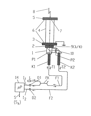
receiving paths are shown. In the sensor set-up in
accordance with Figure la, the light emitted from a light
source (L), for example a laser diode, firstly traverses a
fiber-optic beam splitter or fiber coupler (FK) and then a
fiber cable, preferably a fiber-optic cable (F1), through
which it is transmitted to the sensor head. The light is
collimated there by a 1st collimator (K1) and thereafter
linearly polarized by a downstream 1st polarizer (P1). It
then traverses sequentially a beam splitter (1), 1st and 2nd
glass plates (2, 3) and an electrooptic crystal (4) which is
sealed at the end by an electrically conductive, optically
reflecting, aluminized 3rd glass plate (5). (6) denotes
layer electrodes, the layer electrode on the 2nd glass plate
(3) being an electrically grounded transparent indium tin
oxide layer. (7) denotes a mirror. In the case of the 3rd
glass plate (5), the layer electrode (6) serves
simultaneously as a mirror (7); it consists of a gilded
21~8310
chromium layer which surrounds the 3rd glass plate (5). The
light beam is retroreflected into itself at the 3rd glass
plate (5), with the result that it once again traverses the
electrooptic crystal (4). It is decomposed in the beam
splitter (1) into 2 component beams (T1, T2). A 1st
transmitted component beam (T1) runs via the 1st polarizer
(P1), which now acts as an analyzer, through the 1st
collimator (K1) and the fiber-optic cable (F1) to the fiber
coupler (FK). From there, a fraction of the light determined
by the coupling ratio passes to an optoelectric detector or
to a 1st light detector (D1), which on the output side
supplies an electric signal (I1), proportional to the
received light intensity, to an electronic evaluating system
or a computer or microprocessor (14) at which a measurement
result signal (S) can be tapped at the output side.
A 2nd component beam (T2) reflected at the beam
splitter (1) firstly traverses a phase-delay plate,
preferably a ~/4-delay plate (9), thereafter a 2nd polarizer
(P2), a deflecting prism or 90 prism (10) and a 2nd
collimator (K2) which launches the component beam (T2) into
a 2nd fiber-optic cable (F2). Through this fiber-optic cable
(F2), the component beam (T2) finally passes to a 2nd light
detector (D2) which supplies on the output side an electric
signal (I2), proportional to the received light intensity,
to the microprocessor (14).
The 3 glass plates (2, 3, 5) are not essential to
the principle of the mode of operation of the sensor. In
practice, they serve as holding elements and substrates for
the vapor-deposited layer electrodes (6), to which an
electric voltage or high voltage (8) which is to be detected
is applied. The 1st glass plate (2) serves only as an
intermediate element. In order to keep thermally induced
stresses as small as possible, the glass of the 3 glass
plates (2, 3, 5) should have a similar thermal expansion
coefficient as the electrooptic crystal (4).
In Figure lb, input and output channels are
interchanged by contrast with Figure la.
Figure 2a specifies the angular orientation of the
optical components for the sensor configuration in
214831~
-- 6
accordance with Figure la. The polarization direction of the
1st polarizer (P1) is parallel to one of the two mutually
orthogonal edges (u, v) of the base surface of the beam
splitter (1), whose 3rd edge (w) is orthogonal to the other
two edges. The polarization is therefore parallel or
perpendicular to the optical plane of incidence which is
relevant to the beam splitting (p- polarization or s-
polarization in the polarization directions (x) and (y),
respectively, that is to say polarizations parallel and
perpendicular to the respective optical plane of incidence).
This linear polarization is then maintained during
transmission through the beam splitter (1). Another
orientation of the 1st polarizer (P1) would entail that
there would be a transition of the light into an elliptical
polarization state, since s-fractions and p-fractions
generally experience different phase shifts upon
transmission through the beam splitter (1). 2
electrooptically distinctive 1st and 2nd axes (H1, H2) of
the electrooptic crystal (4) are perpendicular to the beam
direction and also perpendicular to a 3rd distinctive
optical axis (H3) of the electrooptic crystal (4) in the
beam direction. The 1st and 2nd electrooptically distinctive
axes (H1, H2) form a 45 angle with the polarization
direction of the incident light. The end faces of the
electrooptic crystal (4) are likewise perpendicular to the
beam direction. The principal axis of the ~/4-delay plate
(g) is perpendicular to the direction of the light beam
reflected at the beam splitter (1), and forms an angle of
+45 or -45 with the directions of the edges (v, w) of the
beam splitter (1); it is thus simultaneously parallel to the
projection of one of the electrooptic axes of the
electrooptic crystal (4). The polarization direction of the
2nd polarizer (P2) is at 45 to the main axis of the
~/4-delay plate (9). The edges (u, v, w) of the 90 prism
(10) are parallel to the corresponding edges (u, v, w) of
the beam splitter (1).
Figure 2b shows the orientation of the light
components for the sensor set-up in accordance with
Figure lb.
- 2148~1~
Amplitude effects and phase effects:
Effects are considered below which have a
disturbing effect on the relative phase r and a modulation
contrast K1 and K2, respectively, of the electrooptic
signals I1, I2. The conclusions which result therefrom for
the selection, arrangement and angular orientation of the
components are explained.
The most important disturbing effects are:
- The beam splitter (1) introduces different phase shifts
for p-polarizations and s-polarizations, both in
reflection and in transmission.
- Reflectivity and transmission are generally different for
s-polarizations and p-polarizations.
- The 90 prism (10) likewise introduces a phase difference
between s-polarizations and ppolarizations.
Added further to this there may be disturbing
effects caused by an inaccurate ~/4-delay plate (9) and/or
an inaccurate angular adjustment of the components.
The signals I1 and I2 in the two channels can be
represented as:
I1(t) = Io [A1 + B1 cos (r - 1)]/2 and (3)
I2(t) = Io [A2 + B2 cos (r + ~/2 - 2)]/2 , (4)
it being the case that equation (3) holds for the channel
without, and equation (4) holds for the channel with the
~/4-delay plate (9). In this case, A1, B1 and A2, B2
respectively designate coefficients for determining the
modulation contrast K1 and K2, respectively, where
K1 = B1/A1 and K2 = B2/A2, r denotes the electrooptic phase
shift, and 1 and2 denote additional phase terms which lead
to a deviation from the 90 phase shift.
It holds in the ideal case that: A1 = B1 = A2 = B2 =
1 and 1 = 2 =
1st effect of the beam splitter:
In the channel without the ~/4-delay plate (9), the
abovenamed disturbing effects have no effect on the contrast
and the 90 phase shift, if the orientations shown in
Figures 2a and 2b are selected, that is to say it then holds
that A1 = B1 = 1 and 1 = O, and consequently: I1 = Io [1
+ cos r]/2.
- 214831~
-- 8
It holds for the channel with the ~/4-delay plate
(9) and the special case ~1 ~ ~ as = ap that:
A2 = 1, B2 = cos ~1~ 2 = , and thus that
I2 = Io [1 + cos ~1 cos (r + ~/2]/2, (5)
it being the case that as and ap signify the amplitudes of
luminous intensity for s-polarization and ppolarization
after reflection at the beam splitter (1) or after the 2nd
transmission through the beam splitter (1), and ~1 signifies
the phase shift, introduced by the beam splitter (1),
between s-polarization and p-polarization, which is normally
different for reflection and transmission.
The modulation contrast K2 is reduced by a factor of
cos ~1- The 90 phase shift re~;n~ unaffected (2 = )-
The result for the channel with the ~/4-delay plate
(9) and the general case~l ~ 0, as ~ ap is:
A2 = (aS2 + ap2)/2, (6)
B2 = [aS2 ap2 cos2 ~1 + (aS2 - ap2)2/4]0 5 and (7)
2 = arc tan (aS2 - ap2)/(i 2 as ap cos ~1) (8)
The _-sign relates to the orientation of the
~/4-delay plate (9), that is to say to the quick axis under
+45O with respect to the polarization direction (x). In this
case, both the modulation contrast K2 and the 90 phase
shift are affected in principle by the beam splitter (1).
Figure 3 shows the absolute value l2¦ of the error
of the 90 phase shift as a function of the relative phase
delay ~1 of the beam splitter (1) for amplitude ratios
aS/ap = 0.5 or 0.9 or 1Ø It is seen that the relative
phase delay ~1 has no effect on the 90 phase shift (20) if
the amplitudes as, ap for the s-polarization and p-
polarization are equal (line of short dashes). By contrast,
an error is always present for unequal amplitudes, compare
the line of long dashes and the continuous line.
Figure 4 shows the modulation contrast K2 = B2/A2 as
a function of the relative phase delay ~1 for the 3
amplitude ratios aS/ap = 0.5 or 0.9 or 1.0 specified in
connection with Figure 3. The modulation contrast K2 is
impaired only insubstantially almost independently of the
amplitude ratio aS/ap for relative phase delay~1 at the beam
splitter (1) of less than 10.
9 2148310
The following values were measured for a
commercially available cuboid beam splitter (1) with a
metal/dielectric hybrid splitter layer:
Transmission: ~1 = 1, aS/ap = 0.954,
Reflection: ~1 = 6, aS/ap = 1.049.
The spread of the values for different specimens of
this splitter type was slight.
Consequently, the modulation contrast K2 in the
channel with the ~4-delay plate (9) is reduced by the
factors 0.986 (given the ~/4-delay plate (9) in the
transmission path) or by 0.981 (given the ~/4-delay plate
(9) in the reflection branch). The 90 phase shift is
disturbed by the angles ~2 = 2.70 and 2 = 2.71,
respectively. The disturbing effects are therefore
negligibly small.
For beam splitters (1) with an exclusively
dielectric splitter layer, the amplitude ratio aS/ap differs
extremely strongly from 1 and has a correspondingly large
effect on the modulation contrast K2 and the 90 phase
shift, see Figures 3 and 4.
It is preferable to select a type of beam splitter
for which the amplitude ratioaS/ap lies as close as possible
to 1 and the phase delay ~1 lies as close as possible to 0.
If the relative phase delay ~1 differs strongly for
transmission and reflection, the channel with the ~/4-delay
plate (9) is preferably placed into the branch with the
smaller value of the relative phase delay ~1
2. Additional effect of phase error of the ~4-delay
plate (9):
It can occur in practice that in addition to the
disturbing effects just mentioned, owing to the ~4-delay
plate (9) the phase delay deviates from the 90 phase shift
by a phase displacement angle ~3. It then holds for the
coefficients A2, B2 and the 90 error ~2 for the case in
which the 1st polarizer (P2) (analyzer) is aligned parallel
to the polarization direction (y) (s-polarization in
accordance with Figures 2a and 2b) that:
A2 = (aS2 + ap2)/2 - (aS2 - ap2) sin~3/2, (9)
B2 = {aS2 ap2- cos2 ~1 cos 2~3 +
2148~1~
-- 10
[(aS2 _ ap2)-(aS2 + ap2) sin ~3]2/4}o.5 and(10)
~2 = arc tan [(aS2 - ap2) -(aS2 + ap2) sin ~3]/
(+ 2 as ap cos ~1 cos ~3). (11)
If the 1st polarizer (P2) is parallel to the
polarization direction (x), the signs of B2 and ~2 change in
equation (4), that is to say it holds that
2(t) = Io [A2 - B2 cos (r + ~/2 + ~2)]/2. (12)
Consequently, the 2nd sign changes in equation (9),
the 3rd sign in equation (10), and the 2nd sign in equation
10 (11).
Where ~1 = 1 and aS/ap = 0.954, the result for a
phase displacement angle ~3 = 1.8 is a deviation from the
90 phase shift by
~2 = 0-90 for the 2nd polarizer (P2) ¦¦ x or
~2 = 4-49 for the 2nd polarizer (P2) ¦¦ y, respectively.
It may be seen that given these relatively small
disturbing effects, the phase displacement angle ~3 of the
~/4-delay plate (9) is either added to or subtracted from
the 90 error of 2.7 calculated above for ~3 = 0,
depending on the polarization position. The 90 error can
thus be compensated to 0 by a specific selection of ~3.
A rotation of the 1st polarizer (P1) from x to y or
from y to x has no effect on the 90 phase shift or the
modulation contrast.
Disturbing effects which are produced by an
inaccurate azimuthal orientation of the components are not
considered here. In practice, the angular adjustment can be
undertaken so accurately that these disturbing effects play
no role.
3. Effect of the 90 prism (10):
In the case of total reflection, a phase shift of
36.9 for a refractive index of the prism of 1.5 is produced
in the 90 prism (10) between s-polarization and
p-polarization.
If the 90 prism (10) in accordance with Figure lb
is located in the receiving channel without the ~/4-delay
plate (9), this phase shift has no effect on the sensor
signals for the angular orientations specified in Figure 2b.
If the 90 prism (10) in accordance with Figures la and 2a
21~31~
- 11
.
is located in the beam path with the ~/4-delay plate (9),
the ~/4-delay plate (9) and the 2nd polarizer (P2) must be
located upstream of the 90 prism (10), that is to say
between the 90 prism (10) and beam splitter (1). An
arrangement between the 90 prism (10) and the collimator
(K2) would entail the modulation contrast in this channel
reducing by a factor of approximately 0.8.
Figure S shows the relative optical power balance
for the ideal, lossless case and a splitter ratio of 1:1
both at the fiber coupler (FK) and at the beam splitter (1).
The light power launched at the light source (L) into the
fiber-optic cable (F1) is assumed to be 100~. 50% thereof is
left over downstream of the fiber coupler (FK). Since the
light arrives unpolarized at the 1st polarizer (P1), the
light power is halved a further time by the 1st polarizer
(P1) to 25~ of the original light power. After the 2-fold
traversal of the beam splitter (1), the light intensities
are reduced to 6.25~. This is the maximum light power,
corresponding to the maxima of the electrooptic modulation
given by I1(t) and I2(t), which passes into the receiving
channels through the analyzers (P1, P2). In one channel,
this light power is halved a further time by the fiber
coupler (FK), with the result that, finally, at the maximum
of the modulation 3.125~ or 6.25~ of the original light
power is still incident at the light detectors (D1, D2).
If a beam splitter (1) with a ratio of transmission
to reflection of 2:1 is used both for s-polarization and for
p-polarization, the result is that the maximum light powers
incident at the two light detectors (D1, D2) are equal. They
then amount respectively to 5.55~ of the original power,
compare the values specified in brackets.
Figures 6a and 6b show 2 further sensor variants, in
which the transmitting and receiving paths are separate.
Here, as well, each of the sensors requires only one light
source (L). The two 90 phase shifts are, in turn, derived
from a common optical beam path in the electrooptic crystal
(4), with the result that the birefringence of the
electrooptic crystal (4) does not affect the 90 phase
shift. The optical system for generating the 90 phase shift
2148310
- 12 -
is the same as in the case of Figures 1 and 2. Like the 3rd
glass plate (5), the 2nd glass plate (3) has here a layer
electrode (6) transparent to optical signals. The deflection
of the input light beam is performed not by a mirror (7),
but by a 90 prism (11) on the 3rd glass plate (5).
Advantages of these two sensor variants are:
- In the sensor variants in accordance with Figures la and
lb, it is possible chiefly at the 1st light detector (D1)
for a signal background to occur as a consequence of
undesired reflections from the optical system. The reason
for such reflections is steps in refractive index at the
interfaces, in particular in fiber plugs. In the case of
the sensor configurations in accordance with Figures 6a
and 6b, such reflections do not pass to the detectors, or
do so only in a very attenuated form, and are therefore
not particularly disturbing. The quality of the fiber
plugs can be lower.
- The fiber coupler (FK) is eliminated.
- The light power at the light detectors (D1, D2) is higher.
The following disadvantages oppose the advantages:
- An additional fiber-optic connection is required between
the transceiver side and the sensor head.
- A 3rd collimator (K3) and a 3rd polarizer (P3) are
required.
- The transverse dimensions of the optical system are
larger. The necessary minimum cross section of the
electrooptic crystal (4) is therefore likewise larger.
The same holds with reference to amplitude effects
and phase effects as in the case of the sensor
configurations in accordance with Figures la and lb. In
addition, the relative phase shifts in the case of the
2-fold reflection in the 90 prism (11) at the upper surface
of the 3rd glass plate (5) by an angle ~2 between the
s-polarization and p-polarization in each case are to be
considered, the value being ~2 = 36.9 for a refractive
index of 1.5 for the 90 prism (11). In order for these
phase shifts not to have an effect on the relative phase of
the 90 phase shift or the modulation contrast, the edges of
the base surface of the prism should be aligned parallel to
21~8~1~
- 13 -
the electrooptically distinctive axes (H1, H2) of the
electrooptic crystal (4). The two signals of the 90 phase
shifts are then displaced jointly by the same phase angles
2 ~2~ their relative phase remaining unchanged, however.
The signals for the light intensity I1 and I2 are then
given, by modifying equations (3) and (4), by:
I1(t) = Io [A1 + Bl cos (r ~ 2 ~2]/2 and (13)
I2(t) = Io [A2 + B2 cos (r+~/2 -2) - 21~2]/2~ (14)
it being the case that equation (13) holds for the channel
without, and equation tl4) for the channel with the
~/4-delay plate (9).
As is set forth in more detail in the above-named
US-A-4,904,931, the optical phase shift r proportional to
the acting field or to the high voltage (8) can be
determined from these two equations (13, 14). The voltage
amplitude or the measurement result signal (S) being sought
is then determined by calibration as a function of the
optical phase shift r.
The sensor response is not impaired by the zero-
point shift. If it is desired, it can be compensated foragain in the two channels by means respectively of an
additional delay plate with a delay of 2 ~2.
If the 90 prism (11) were to be aligned with the
edges at 45 to the electrooptically distinctive axes
(H1, H2) of the electrooptic crystal (4), the relative phase
delays of the 90 prism (11) would entail additional
disturbing effects.
In order to avoid the additional 90 prism (11), it
would be possible to make the input light beam extend
slightly obliquely relative to the 3rd electrooptically
distinctive axis (H3) of the electrooptic crystal (4) and
then to cause it to be reflected again at a mirror surface
(7) of the 3rd glass plate (5), in accordance with the beam
paths (12) illustrated in Figure 7. (13) denotes an optical
system composed of beam splitter (1), ~/4-delay plate (9),
polarizers (P1, P2, P3), collimators (K1, K2, K3) and 90
- prism (10).
The optical power balance is the same for both
sensor configurations, and is represented in Figure 8 for
21~8~10
- 14 -
the ideal, lossless case. 25~ of the original optical power
arises respectively at the two light detectors (D1, D2) at
the maxima of the optoelectric modulation.
The light source (L) should preferably have a short
coherence length, so that, for example, no interference
effects occur in the event of multiple reflections within
the sensor optical system. Owing to increased noise, these
could have a disturbing effect on the measured light
intensities I1 and I2. It is preferable to use a light-
emitting semiconductor diode (LED) or a multimode laser
diode.
The fiber-optic connections are multimode fiber
cables (Fl, F2). When a laser diode is used as the light
source (L), the fiber-optic cable (F1) for the transmitting
path is to be selected to be at least so long (normally a
few 10 m) that the light arriving at the sensor head is
adequately depolarized and satisfactorily incoherent, in
order to suppress signal fluctuations and noise as a
consequence of polarization fluctuations and interference
effects. In the case of separate transmitting and receiving
paths in accordance with Figures 6a and 6b, a monomode fiber
(F3) maintaining polarization is also suitable for the
transmitting path when a multimode laser diode is selected
as the light source (L). With a light-emitting semiconductor
diode, the optical power launched into the monomode fiber
would be too low. The fiber axes must then be aligned at the
sensor head in such a way that the polarization direction
lies parallel to the transmission direction of the input
polarizer (P3).
In the case of combined transmitting and receiving
paths in accordance with Figures la and lb, it is rather the
case that a monomode fiber is unsuitable, since for
relaunching the light into the fiber the requirements placed
on the mechanical stability of the sensor set-up would be
rendered drastically more stringent because of the small
diameter of the fiber core.
Crystal classes and crystal orientations which are
suitable for a line integration of the electric field and
2148~10
- 15 -
which are not birefringent without an applied electric
voltage are specified in the following Table 1.
Table 1:
s
Crystal axis Directions of
Classparallel to the the principal Materials
light propagation electrooptic axes
(H3)
43m (Td) 4-fold axis [110] and [110] Bi4(SiO4)3 (BSO)
[001] Bi4(GeO4)3 (BGO)
ZnS, ZnSe, CuCl
42m(D2d) 4-fold axis [110] and [110] Potassium dihydrogen [001] phosphate
KH2P04 (KDP)
23(T)2-fold axis [110] and [110] Sodium chlorate
[001] NaC103
Here, the crystal classes are denoted by their international
and, in brackets, also by their Shoenflies notation.
The two crystal classes specified in Table 2 are
already birefringent without an electric field. The
principal axes of the intrinsic birefringence coincide with
the principal electrooptic axes, with the result that the
intrinsic birefringence is added to the field-induced
birefringence simply as a constant, unchanging system
deviation.
- 16 - 214831~
Table 2:
Crystal axis Directions of
Class parallel to the the principal Materials
light propagation electrooptic axes
(H3)
_ ¦¦ and 1
6m2 (D3h) 2-fold axis 3-fold axis LiNaC03
2mm (C2v) 2-fold axis [100] and [010] MgBaF4
[001]
There are in addition other crystal classes, which would
basically also be suitable for integration, but in which the
axes of the intrinsic and of the field-induced birefringence
have different directions. These crystal classes will
therefore not be considered in more detail.
It is important that light enters the electrooptic
crystal (4) with a polarization which differs from 0 and
90, preferably in the range of 40-50, in particular below
45 relative to an electrooptically distinctive axis (Hl).
After a 2-fold traversal of the electrooptic crystal (4)
(there and back), the light is decomposed at the beam
splitter (1) into 2 component beams (Tl, T2). Located in the
1st component beam (Tl) is the 1st polarizer (Pl) which acts
as an analyzer for this channel. The 2nd component beam (T2)
runs via the ~/4-delay plate (9), which produces the 90
phase shift between the two channels, and then likewise via
an analyzer (P2). The light beam reflected at the beam
splitter (1) is additionally directed via the 90 prism
(10), resulting in parallel beam directions for the two
channels. This enables a compact design. The properties,
orientation and arrangement of the optical components are
selected such that for s-polarization and p-polarization in
the case of transmission and reflection at interfaces (beam
splitter (1), 90 prism (10)) the different phase shifts do
not substantially affect the phase difference between the
two channels and the modulation contrast.
Temperature compensation: -
- 17 - 21~8~1~
The detected electrooptic signals or light
intensities I1 and I2 are usually temperature-dependent. In
the case of Bi4(GeO4)3 (BGO), for example, the temperature
coefficient of the decisive electrooptic coefficient is
approximately 2.4 10 4 K 1, that is to say given a
temperature increase by 100 K, the signal increases by 2.4~
for a constant applied voltage. An additional temperature
measurement is therefore required for an accurate voltage
measurement. In order to avoid a separate temperature
sensor, use is made of a ~/4-delay plate (9), the delay of
which is dependent on temperature to a suitable extent. The
temperature of the ~/4-delay plate (9) and its immediate
environment can then be determined by measuring the phase
difference (~) of the two electrooptic signals (I1, I2).
The voltage or measurement result signal (S) can then be
appropriately corrected.
For a ~/4-delay plate (9) of 0th order made from
quartz, the delay varies for a wavelength of 633 mm by
approximately 0.5 when the temperature changes by 50 K. A
greater temperature dependence can be achieved by using a
~/4-delay plate (9) of higher order, since the temperature-
induced phase change grows in proportion to the order
number. For a ~/4-delay plate (9) having, for example, 2.25
orders, that is to say having a relative delay of 2.25
wavelengths, the delay varies by approximately 4.5 when the
temperature changes by 50 K.
The determination of the phase difference (~)
between the two electrooptic signals (Il, I2) is explained
with the aid of Figure 9, in which these electrooptic
signals (Il, I2) are represented as a function of time (t).
The phase difference (~) between the two electrooptic
signals (Il, I2) corresponds to the delay introduced by the
~/4-delay plate (9). Said delay depends on temperature. The
phase difference (~) can be determined directly from
measurement of the instants tO, tl and t2 of the passages of
I2 and Il through ImaX/2 in accordance with:
= 180 (tO - tl)/(t2 - tl). (15)
The deviation of the phase difference (~) from 90 is
therefore: ~ - 90.
- 18 - 2148~1~
The ~/4-delay plate (9) is to be designed such that
is 90 at room temperature (293 K), and therefore
= o. ~' is then dependent as follows on absolute
temperature T:
~'(T) = ~ (T - 293), (16)
r being the temperature coefficient of the ~/4-delay plate
(9). ~ = O.OgO K-l for a ~/4-delay plate (9) (17)
having 2.25 orders.
The temperature T of the sensor head can then be
determined in kelvins in accordance with:
T = ~'(T)/~ + 293. (18)
The temperature T which is now known can be used to
correct the signal (S) obtained by the microprocessor (14)
from the electrooptic signals (I1 I2) with respect to
temperature T in accordance with:
Sk = S ~(T), (19)
it being the case that ~(T) is given as
~(T) = 1 + (T - 293). (20)
iS the temperature coefficient of the electrooptic phase
shift. iS approximately 2.4 104 K~1 for Bi4(GeO4)3
(BGO).
The sensor is to be calibrated so as to produce the
desired signal (S) for T = 293 K with ~(293 K) = 1. For the
case in which the sensor is used for force measurement (see
further below), use is to be made in equation (20) of the
temperature coefficient of the mechanically induced
birefringence.
In the case of crystals of classes 6m2 and 2mm,
which have an intrinsic birefringence, the temperature
dependence of this birefringence can be used for temperature
measurement. A change in the birefringence leads to an
additional, slow phase shift in the two electrooptic signals
(I1, I2). This phase shift is equally large for both
electrooptic signals (I1, I2). In addition, there is the
temperature-dependent change in their relative phase on the
basis of the temperature dependence of the ~/4-delay plate
(9), which is, however, negligibly small by comparison with
the absolute shift.
- 19 2148310
The slow phase shift, which depends on temperature,
can be determined in increments of 90 from the overall
number of zero-crossings occurring for the two electrooptic
signals (I1, I2). If the zero-crossings are counted with a
positive sign in the case of a positive phase shift, and
those relating to a negative phase shift are counted with a
negative sign, the total number of the accumulated zero-
crossings which are caused by the applied alternating
voltage (8) is 0 after each full period of the alternating
voltage (8). All the additionally occurring zero-crossings
are to be ascribed to temperature changes or DC voltage
components. The number of the zero-crossings owing to DC
voltages is, however, negligibly small by comparison with
temperature-induced zero-crossings.
The phase shift owing to the intrinsic birefringence
is given in the case of a 2-fold passage of the light
through the electrooptic crystal (4) as:
~r=4 ~ L an/~ t21)
where L = crystal length, ~ = wavelength of the light, and
~n = difference between the refractive indices in the case
of birefringence.
In the case of a temperature change ~T, the phase
changes by
~r(~T) = ~r I r~n . ~T. (22)
r~n = ~n/(~n ~T) is the temperature coefficient of the
birefringence.
~ r (~T) is yielded from the number N(~T) of the
additional zero-crossings in increments of ~/2 or 90 in
accordance with:
~r(T) = N(~T) ~/2. (23)
The temperature dependence is therefore:
~T = [N(~T) ~]/(2 ~r r~n) (24)
Only temperature changes can be measured in the case
of this method. The initial temperature Ta must be input
anew for each commissioning of the sensor. It then holds
that:
T = Ta + ~T- (25)
Example:
- 20 - 2148~10
For birefringence with ~n = 0.01, a temperature
coefficient of birefringence f ~n = 10-4 K-1, a crystal
length L = 10 cm, a wavelength ~ = 780 nm and a 2-fold
passage of light through the electrooptic crystal (4), the
result is:
- a total phase shift ~r = 1 . 6 104 rad and, (26)
- a phase shift, in the case of a temperature change by AT,
of:
~r = 1 . 61 ~T. (27)
The result for ~T = 1 K is ~r = 1 . 61 rad or 92.
The sensor can basically also be used for a dynamic
optical measurement of pressure or force. A possible
configuration is represented in Figure 10. A force (15) acts
here parallel to a light propagation direction (X1). Given a
suitable choice of the crystal class and crystal
orientation, the electrooptic crystal (4) is birefringent
for light which propagates along the light propagation
direction (X1). In the case of a cubic crystal (4) of
classes 23 (T) or m3 (Th), one light propagation direction
(X3) is to coincide with one of the 3 cube axes. The 3
principal refractive indices for the polarization directions
parallel to the cube axes then change in accordance with:
~n1 = - no3 ~11 ~/2,
~n2 = - nO3 ~13 ~/2,
~n3 = - no3 ~12 ~/2,
nO signifying the refractive index without an applied force
(15), ~ signifying the applied force (15) per face, and ~ij
signifying the photoelastic coefficients. ~12 = ~13~ and
thus ~n2 = ~n3 for an electrooptic crystal (4) which belongs
to one of the 3 other cubic classes 43m, 432, m3m (Td, O,
n). These classes are therefore not suitable for measuring
pressure in the configuration in accordance with Figure 10.
The birefringence is given by:
~n = ~n2 - ~n3 = -no3 (~13 ~ ~12) ~/2
for classes 23 and m3.
The polarization direction of the incident light
preferably forms a 45 angle with the X2- and X3-axes. The
resulting phase difference, which is accumulated by the two
orthogonal polarization components parallel to X2 and X3 in
- 21 - 21~31~
the case of 2-fold passage of the electrooptic crystal (4)
of length (L), is given by equation (26).
Example:
The difference ~13 ~ ~12 is usually of the order of
S 10-12 m2/N. The result with nO = 2, L = 0.1 m, ~ = 106 N/m2
and ~ = 780 nm is ~r = 6.44 rad or 369.
It would also be possible to use noncubic crystal
classes for the measurement of force.
It would also be possible, in accordance with Figure
11, to exert the force (15) transversely onto a glass rod
(16), represented in cross section, instead of
longitudinally onto an electrooptic crystal (4). The
polarization (P) of the incident light would have to lie
here preferably at 45 relative to the direction of the
force (15). (H1) and (H2) designate principal axes of the
induced birefringence.
Obviously, numerous modifications and variations of
the present invention are possible in light of the above
teachings. It is therefore to be understood that within the
scope of the appended claims, the invention may be practiced
otherwise than as specifically described herein.