Note: Descriptions are shown in the official language in which they were submitted.
CA 02148450 2000-10-13
-1-
ELECTROSTATIC SPRAY DEVICE WITH PHOTOELECTRIC SWITCHING MEANS
This invention relates to electronic switching means for use in
applications involving high voltages of at least 1 kV and more
usually at least 5 kV ranging up to 50 kV.
Although not limited thereto, the invention has particular
application to devices for effecting electrostatic spraying of
materials, especially liquids. Typical devices of the type that the
present invention is concerned with are disclosed in EP-A-120633,
EP-A-441501, EP-A-468735 and EP-A-468736.
According to one aspect of the present invention there is
provided electronic switching means comprising a series of radiation
sensitive semiconductor junctions collectively having a mazimum do
reverse voltage of at least 1 kV (preferably at least 5 kV and often
at least 10 kV), terminal means for the application of high voltage
to the junctions such that the junctions permit current flow in one
direction only when forwardly biased by an spplied voltage, and
selectively operable, radiation producing means associated with said
junctions for selectively irradiating the same so as to produce
current flow in the reverse direction when the junctions are reverse
biased by as applied voltage, said junctions and the radiation
producing means being supported in fazed predetermined relation
within a mass of encapsulating materiel transmissive to the radiation
emitted from the radiation producing mesas.
Preferably said junctions collectively have a mazimum do reverse
voltage of at least 5 kV and more preferably at least 10 kV.
It is to be understood that, when said series of junctions are
reverse biased sad not ezposed to radiation from said radiation
producing means, there may nevertheless be a small current floss as in
the case of a conventional diode (dark current) but the reverse
current flow is neglible compared with that produced when the
junctions are forwardly biased with a voltage of the same amplitude
but opposite polarity. In contrast, when the junctions are reverse
biased and subjected to irradiation, the current flow is
substantially greater than that occurring in the absence of such
irradiation.
The encapsulating mass may be such as to provide reflective
surfaces in the vicinity of the junctions so that radiation which is
PCT/GB93102403
WO 94/13063
;q(~ f" ;~
-2-
not directly incident on the junctions is reflected thereby
increasing the efficiency with which the junctions is irradiated.
Such reflective surfaces may be constituted by a specific layer or
layers of material reflective to radiation at the~wavelength or
wavelengths emitted by the radiation producing means; or reflectivity ,
may be obtained as a result of changes in refractive index within the
mass of encapsulating material.
It is widely known that silicon diodes having a pn junction are
photosensitive and that, when reverse biased and exposed to near
infrared radiation, such diodes are rendered conductive and permit
current flow substantially in excess of the dark current. This is the
principle underlying photodiode operation. In contrast with
conventional photodiodes which have an architecture or layout
consistent with making effective use of incident light, the switching
15 means according to said one aspect of the invention is_ designed to
operate at voltages substantially in excess of those at which
conventional photadiodes are intended to operate. Thus, conventional
photodiodes are designed with marimum do reverse voltages ranging up
to 600 volts (see "Optoelectronics", D.A.T.A. Digest 1992 (Edition
20 25) published by D.A.T.A. Business Publishing of Englewood, Colorado,
USA - "Photodiodes", Page 613) whereas the switching means of this
aspect of the invention is intended for use in applications involving
high voltages of at least 1 kV, and more usually at least 5 kV
ranging up to for example 50 kV.
25 In a preferred embodiment of the invention, said series of
semiconductor junctions constitute a high voltage semiconductor
diode, preferably a high voltage silicon diode having a series of
stacked pn junctions.
The radiation producing means conveniently comprises a
30 light-emitting diode. As used herein, references to "light" are to be
understood to encompass electromagnetic wavelengths lying outside the
visible part of the spectrum as well as wavelengths within the '
visible spectrum. For instance, a suitable form of ligr.t-emitting
diode produces an output in the near infrared ead the high voltage
35 diode forming said series of junctions may be sensitive to such
radiation.
~~'~'~ WO 94/13063 _ ~ ~ ~ ~ '~ ~ ~ I'CT/GB93/02403
-3-
Although the components forming the switching means of the
present invention may be fabricated in the form of a large scale
integrated circuit, the invention includes within its ambit
fabrication of the switching means from discrete components.
Accordingly, a second aspect of the present invention provides a
method of fabricating electronic switching means as defined
hereinabove, in which a high voltage semieonductor diode and a solid
state light-emitting source are assembled in predetermined relation
such that the series of junctions of the diode are exposed to light
emitted by said source, and encapsulating the so related diode and
source in an encapsulant material Which is transmissive to the light
emitted by the source.
The predetermined relation will usually involve positioning of
the source in close proximity with the diode junctions in such a way
that a substantial part of the light emitted by the source will be
incident on the diode junctions.
This aspect of the invention may be implemented using
commercially available discrete components. Commercially available
high voltage diodes have an architecture or layout, ie. a series of
stacked pn junctions (typically in excess of ten such junctions and
often twenty or more) appropriate for manage~ent of high potential
and are fabricated without regard to light-induced effects using
encapsulant materials which are not particularly suited to permitting
exposure of the junctions to external radiation; indeed, this is
generally considered highly undesirable.
Thus, in accordance with this aspect of the invention, the diode
may comprise a conventional commercially available high voltage diode
encapsulated in an electrically insulating material, in which case
the diode selected may be one having an encapsulating materiel which
already has substantial transmissivity with respect to the wavelength
of the light emitted by the source or alternatively the source may be
selected so as to be compatible with the diode encapsulating material
in terms of transmissivity of the latter with respect to the
" wavelength of light emitted by the source.
Where the commercially available diode is one having an
encapsulating material which is opaque or has relatively low
transmissivity with respect to the light emitted by the source, the
f
WO 94/13063 ~ ~ ~ ~ ~ ~ ~ PCTlGB93102d03
-4-
method of the invention comprises modifying the. diode encapsulating
material to impart, or enhance, effective light coLpling between the
source and the series of junctions of the diode. ,
Such modification may involve at least partial removal of the
diode encapsulating material or some form of treatanent to enhance the
light transmissivity of the encapsulating material. Fos instance, one
form of high voltage diode in widespread use is encapsulated in a
glass material, the transmissivity of which can be modified by heat
treatment.
According to a further aspect of the invention there is provided
a high voltage generating circuitry producing an output voltage of at
_ least 1 kV, more usually at least 5 kV, at output terminal means
thereof, said circuitry incorporating an electronic switching means
as defined hereinabove operatively associated with the output
I5 terminal means.
This aspect of the invention has particular application to high
voltage genezating circuitry adapted to be powered by a low voltage
source such as a battery supply.
In one embodiment thereof, the circuitry is arranged to produce
a unipolar high voltage output and the electronic switching means is
coupled to the output terminal means in such s way that said series
of junctions are reverse biased by said unipolar output voltage.
In another embodiment thereof, the circuitry is operable to
produce an alternating high voltage output, said switching means
being coupled in the circuitry in such a way as to rectify said
alternating output voltage to produce at the output terminal means 8
high voltage of one polarity, the arrangement being such that s8id
series of junctions is reverse biased by the opposite going polarity
cycles of the alternating' output v4ltage.
In a further embodiment, the circuitry is operable to produce an
alternating high voltage output and a pair of said switching means is
associated with the output terminal means, each switching means being .
arranged such that one switching means is reverse biased and the
other forward biased by the positively going cycle of the alternating
voltage and vice versa by the negatively going cycle, means being
provided for controlling operation of the radiation producing means
of each switching means to render each switching means conductive in
y.~,..
'''.'~~' WO 94113053
PCTlGB93I~?.403
_5_
the reverse biased condition thereof. The switching means in such an
embodiment may be in series or in parallel with each other.
In yet another embodiment, the circuitry comprises a pair of
output terminal means at each of which a unipolar.output is produced,
the output at one terminal means being of opposite polarity to that
produced at the other terminal means, and a pair of said switching
means associated with said output terminal means and connecting each
output terminal mesas to a common terminal means but being reverse
biased by the respective unipolar output, means being provided for
controlling the radiation producing sources of the switching means in
such a way that the switching means are alternately rendered
conductive whereby a bipolar output is produced at said common
terminal means.
Although the present invention in its broader aspects is not
limited thereto, electronic switching meanslhigh voltage generating
circuitry as defined above is particularly applicable 'to relatively
low current cansumption devices in which the maximum reverse current
conducted by the series of junctions is preferably no greater than
10 ~.A, and more preferably no greater than 2 ~i.A.
According to another aspect of the present invention there is
provided an electrostatic spraying device ccl~hprising a housing,
nozzle means, means for supplying to the nozzle.means a material to
be sprayed from the nozzle and high voltage generating circuitry for
directly or indirectly applying to the material high potential
~5 whereby the sprayed material is electrostatically charged, said
circuitry including electronic switching means as defined hereinabove
associated with the high voltage output of the circuitry and arranged
to control current and/or voltage stitching operations of the device.
The electronic switching means of the invention is particularly
suitable for electrostatic spraying~devices of this type especially
where current consumption is iow (typically no greater than 10 ~.A,
and more usually no greater than 2 ~.A) and where factors such as
compactness and cheapness are at a premium. Conventional photodiodes
are totally unsuitable since they ar.e only capable of use at low
voltages and are in any event conventionally only considered in
applications involving signal handling as opposed to current handling
applications. Most commercially available high voltage switches are
WO 94113063 ~ ~ ~ g ~ ~ ~ PCT/GB93/02403
_6_
geared towards high current applications (eg switchgear) and are
mechanical.in nature, bulky, expensive and totally unsuited for
spraying devices of the type just referred to. Reed relays are widely
available for low current switching applications but are relatively , '
expensive being electromechanical in nature with high input
requirements and short lifetimes and have upper limiting voltages of
the order of I2 kV. Any mechanically based switching device is
subject to size constraints due to the need for separation of
components at elevated voltages.
In one embodiment of the spraying device, the switching means is
operable to provide a current discharge path in response to
de-energisation of the high voltage generating circuitry. In this
instance, the switching means may be reverse biased by the high,
voltage during spraying operation of the device, and the arrangement
~y be such that, in response to de-energisation of the circuitry,
the radiation producing means is operated to irradiate. the switching
means and thereby render the latter conducting so as to provide a
path for discharge of current from any capacitively stored electrical
charge at the high voltage output side of the circuitry. The
capacitive component may be constituted by capacitance associated
with the high voltage circuitry and/or capacitance associated with
the load to which the output voltage of the circuitry, eg. a metal
can containing liquid, such as paint, to be sprayed.
The switching means, when used in this manner, obviates the need
for a resistive element at the output side of the circuitry for the
purpose of discharging any capacitively stored charge which, if not
discharged at the time of de-energisation of the high voltage
circuitry, gives rise to a risk of electric shock being experienced
by the user. The use ofsuch a resistive element constitutes a
current drain during spraying and the high voltage circuitry must
therefore be designed to take such current drain into account, with
the consequence that the circuitry necessarily has to produce a
current output in excess of that strictly required for spraying
purposes.
In the interests of compactness and cheapness, it is desirable
to avoid current drain of this nature. This is particularly the case
for hand held or readily portable self-contained spraying devices of
rsly.
-.A :r w 2 ~. ~ ~' '-' '~' ~ .
~'~ WO 94/13063 a ~~ =~ PCTIGB93I02,403
_7_
the type intended to be powered by a low voltage battery supply, for
example hand held devices for spraying. of personal care and hygiene
compositions such as fragrar_ces, deodorants and the like, or hand
held devices for spraying of paint compositions, or portable free
standing devices for spraying room freshener and aromatic
compositions. Where a low voltage battery supply is employed,
unnecessary power consumption should obviously be eliminated as far
as possible in order to prolong battery life. Also, for reasons of
economy, the output requirements of the high voltage circuitry design
will desirably be minimised to permit the use of inexpensive circuit
designs. The switching means of the invention is particularly
suitable where the above constraints apply because the current drain
is limited to the dark current component (which is negligible in
practice) and, when the high voltage circuitry is disabled, the
switching means may be rendered conductive in the reverse bias
direction to effect discharge of stored charge.
In this embodiment of the invention, the switching means may be
rendered conductive automatically in response to operation of a
user-actuable switch for de-energising the high voltage circuitry and
discontinuing spraying. Thus, the device conveniently includes
user-actuable means for selectively energisi'~g and de-energising the
high voltage circuitry and control means for.triggering emission of
radiation by the radiation producing means to render the switching
means corxductive in response to operation of the user-actuable means
to effect de-energisation of the high voltage circuitry.
Conveniently the switching means may, when arranged to afford a
path for discharge of capacitively stored charge, be coupled into the
high voltage circuitry in such a way as to provide rectification. For
instance, in this event; the high voltage circuitry may include a
step-up transformer with one side of the secondary thereof tapped to
provide an alternating high voltage output and the other side of the
secondary connected to a low potential such as earth, and the
switching means may be connected in series with the secondary to
rectify the alternating voltage and thereby produce a unipolar high
voltage output which may be subjected to capacitive smoothing to
remove or at least substantially attenuate high voltage peaks. In
such an arrangement, when the circuitry is de-energised, charge
,: a
WO 94/13063 ~ PCTlG~93/02403 '''
21~~~~~~~ _~_
stored by the capacitive smoothing component is discharged to said
low potential (eg earth) by rendering the switching means conductive
in the reverse bias direction and the switching means may be placed -
in this condition automatically in response to de~gnergisation of the
high voltage circuitry.
According to yet aaother aspect of the present invention there
is provided an electrostatic spraying device comprising a housing,
nozzle means, means for supplying to the nozzle means material to be
sprayed, high voltage generating circuitry having an output terminal
via which high voltage is applied to said material to effect
electrostatic spraying thereof, an annular element encircling the
nozzle means and on which a high voltage of the same polarity as that
applied to said material is established during spraying to modify the
field intensity in the immediate vicinity of the nozzle outlet. and
means operable upon cessation of spraying to discharge electrical
charge stored by capacitive elements of the device during spraying. .
This aspect of the invention has particular application to the
spraying of liquids which have relatively high viscosity and low
resistivity, may contain suspended solids, eg paint formulations, and
tend to be difficult to spray satisfactorily at flow rates up to at
least 4 ccl~.n using previously developed technology. Typically, the
liquid to be sprayed has a viscosity of at least 0.5 Poise, eg 0.5 to
10 Poise and a resistivity between 5 x 10⁵ and 5 x 10~ ohm. cm.
Said discharge means preferably comprises a switching means as
referred to hereinbefore and the voltage generating circuitry is
operable to produce an output voltage of at least 25 kV. Voltages of
this magnitude are necessary when the liquid to be sprayed is
relatively viscous andlor where there is a requirement for a wide
range of flow.rates; such voltages are, normally considered to be in
excess of those that can be employed without giving rise to spurious
spraying effects believed to be attributable at least in part to
corona discharge effects. Also, operation with voltages of this
magnitude lead to capacitive storage of large amounts of electrical
charge giving rise to the possibility of the user receiving an
unpleasant shock in certain circumstances. The combination of
features forming this last mentioned aspect of the invention allows
large voltages t~ be used whilst securing satisfactory spraying of
E:.
__ ~,O ~~/13063 ~ ~ ~ ~ ~ ~CTIG~93/aZ403
-g_
relatively viscous, law resistivity liquids such as paint
formulations and affording the user protection against discharge of
capacitively stored charge.
Usually an electrostatic spraying device as referred to in any
of said aspects of the invention will be powered by a low voltage
source, such as a battery pack, connected to the input side of the
high voltage generating circuitry and the device will often be in the
form of a portable self-contained unit which may be adapted to be
held in the hand.
It will be understood that the electrostatie spraying devices
disclosed herein are suitable for the spraying of a wide variety of
materials, eg. personal care or hygiene compositions, aromatic
compositions suitable as air fresheners, paint formulations,
insecticides, bactericides and medical preparations. The invention
accordingly includes Within its ambit electrostatic spraying devices
as disclosed herein when fitted with a cartridge containing any one
of these materials.
Various other features and aspects of the invention will become
apparent from the appended claims and the following description, by
way of example only, of various embodiments ~f the invention
illustrated in the accompanying drawings.
In the accompanying drawings:
Figure 1 is a schematic view showing one embodiment of a light
sensitive high voltage electronic switching means in accordance with
the invention;
Figure 2 is a diagrammatic view of an electrostatic spraying device
incorporating high voltage generating circuitry embodying an
electronic switching mews of tie form ahawn in Figure 1;
Figure 3 is a diagrammatic view of a modified form of the embodiment
shown in Figure 2;
Figure 4 is a diagrammatic view of circuitry for generating a bipolar
high voltage output for use in for example an electrostatic spraying
device requiring a bipolar output for shack suppression and/or
a
permitting the spraying of targets which ordinarily are difficult to
spray, eg. targets of electrically insulating material;
PCTIGB93/024t13 ~'~"',
WO 94/13063
_ 2~~~~~~ -10-
Figure 5 is a schematic view of circuitry for providing a high
voltage output and selectively routing the output to a number of
autput devices;
Figure 6 is a schematic view of one form of spray gun to which the
arrangement of Figure 2 or 3 may be applied.
Referring to Figure 1. a switching element in accordance with
the invention comprises an eztra high tension diode 10 which may
typically be constituted by a Philips EST diode, Part No. gY713
(available from RS Components Limited, Part No. RS 262-781). This
diode is a silicon diode comprising a series of stacked pn junctions
encapsulated in a mass of encapsulating material P1 (herein called
the primary encapsulant) and designed for use in high voltage
applications, the maximum do reverse voltage of the diode being
24 kV. A light source in the form of a light-emitting diode (LED) 12
also encapsulated in a mass of encapsulating material P2 (primary
encapsulant, but not necessarily the same material as the material
P1) is mounted in close prozi.mity with the EHT diode 10 so that the
light emitted by the LED 12 when energised is incident on the EHT
diode lo. Typically the LED 12 is constituted by a high powered
infrared emitting LED such as that available from RS Components
Limited, Part No. RS635-296. Both the EHT diode 10 and the LED 12 are
encapsulated as supplied. Where the switching element.of the present
invention is fabricated from discrete components as in the case of
Figure 1, selection of an EHT diode with an encapsulant having at
least some degree of transmissivity With respect to the wavelength of
light produced by the LED is advantageous. Thus, we have found the
above combination of components advantageous since the Philips BY713
EHT diode as supplied has a glass encapsulant which is transmissive
with respect to the wavelength o,f IR produced by a RS635~296 LED.
During fabrication, the EFiT diode 10 and LED 12 are assembled in
optically aligned relationship to ensure that the IR emitted by the
LED 12 is fully effective in irradiating the pn junctions of the
diode 10, taking into account the fact that the architecture of the
diode 10 is aimed at high voltage management rather than light ,
collection (as in the case of a photadiode). The EHT diode 10 and LED
12, once suitably aligned, are then encapsulated in a mass 14 of
material (secondary encapsulant S) having appropriate transmissivity
'v°'' WO 94113063 ~ ~ ~ ~ PCTlGB93/02403 ;
-11-
with respect to the wavelength of emission of the LED. The
encapsulating mass 14 is moulded around the diode 10 and LED 12 in
such a way as to avoid the development n~ air gaps at the respective
interfaces and which would tend to act as reflective boundaries. This
can be readily achieved by adopting a moulding technique which
ensures that any shrinkage that occurs during curing of the
encapsulating material takes place at the outer peripheral surface of
the mass 14 rather than at the interfaces with the diode 10 and LED
12. To avoid deleterious boundary effects, the encapsulating material
forming the mass 14 is selected so as to provide at least reasonable
refractive index matching with the encapsulating materials of the
diode ZO and LED 12. In the ease of the specified components (the
BY713 diode and RS63S-29b LED), suitable encapsulating materials are
the light curing resin LUXTRAR LCR 000 (LD7CTRAR is a RTM of Imperial
Chemical Industries Group of companies) and the W curing resin
RS505-202 available from RS Components. The secondary encapsulant S
additionally serves to provide a high degree of electrical insulation
between the diode 12 at low voltage and the HT diode 10 at high
voltage.
As indicated above, it is important that the moulding procedure
for encapsulating the diodes 10 and 12 in thaesecondary encapsulant S
is conducted in such a way as to ensure that the radiation emitted by
diode 12 is used efficiently. In particular, care must be taken
prevent the formation of interlayer voidages between the primary and
secondary encapsulants. Such voidages tend to arise as a result of
internal stresses set up as the secondary encapsulant shrinks on
curing. This can be achieved by applying a release agent to the mould
to prevent the secondary encapsulant adhering to the sides of the
mould so that he curing~secondary encapsulant preferentially adheres
30' to the primary encapsulant during shrinking rather than to the mould
surfaces. Alternatively, instead of using a release agent, the mould
may be lined with a flexible film liner to prevent the secondary
encapsulant adhering to the mould~surfaces.
As mentioned previously, the architecture of conventional high
voltage diodes is not geared to making effective use of incident
light; indeed many high voltage diodes are encapsulated in material
which is effective to shield the pn junctions from light exposure. In
~, .
WO 94113063 PCTIGB93/02403 "=
_12_
contrast, the present invention seeks to exploit the known affect
that light has on pn junctions and, where the switching element of
the invention is fabricated using a commercially available discrete
high voltage diode, rather than shielding the diode from light
exposure, it is desirable to ma~ci,mise light exposure given that the
architecture is not optimised for light collection. Thus, where
enhancement of the light exposure is needed, in addition to locating
the LED 12 in close proximity with, and in an optimal orientation
relative to, the EHT diode 10, provision is made of a reflecting
surface or surfaces to re-direct light which is not directly incident
on the EHT diode.
In the illustrated embodiment, this is implemented by means of a
layer or coating of material 16 which encompasses the EHT diode 10
and LED 12 and serves to reflect light towards the sites on the EHT
diode at which light exposure is required. ht least past of the
layerlcoating 16 is conveniently of approacimately spherical contour.
The leyer/coating 16 may for instance be composed of MgG.
The assembly of EHT diode 10, LED 12 and encapsulating mass 14
is enclosed in a mass of potting compound 18 (tertiary encapsulant)
which has good electrical insulating properties and encloses the
A
assembly in such a way as to leave the leads 20 of EHT diode 10 arid
electrodes 22 of LED 12 exposed for connection to external circuitry
while shielding the diode 10 ~rom ambient light. If the tertiary
encapsulant is appropriately selected, it is possible to dispense
with the separate reflecting layer 16; for example, the tertiary
encapsulant 18 may be a white reflective material, such as that
available from RS Components, Part No. RS552-5fi8.
The shape and dimensions of the assembly are selected in such a
way that suitable electrical insulation is provided between the low .
3G voltage at which the diode 12 operates and the much higher voltage at
which the ET diode 10 operates. Where for instance only a secondary
encapsulant is used (with or without the reflecting layer 16), the
_ shape and dimensioning of the secondary encapsulant is selected so
that the distances between the high and low voltage leads 20, 22 as
measured across the exposed surface of the secondary encapsulant is
at least 3 mm for each kV applied to the HT diode 10. If however the
assembly is encapsulated Within a potting compound (for instance
~n~, ~~~~~~.5=~i
PCT/GB93102403
~''r"~ WO 9413063
-13- " ~ .
along with other components collectively forming an electrical
circuit with the assembly comprising diodes 10 and 12), the. external
surface of the secondary encapsulant is not exposed to air and the
shaping and ditaensioning in this case is such as to allow a distance
between leads 20, 22, measured across the ezternal~surface of the
secondary encapsulant, of at least 1 mm for each kV to be applied to
the diode 10.
In the case of a RS635-296 LED, the threshold voltage of about
1.3 V has to be exceeded to produce the light necessary to render the
high voltage diode conducting in the reverse direction. The LED
typically only requires 1 mA to open the switch but it is preferred,
especially when used for the production of a bipolar output as
described hereinafter with reference to Figure a, that the initial
peak current to the LED should be up to about 300 mA to afford
maximum current carrying capability, followed by a current supply of
5-30 mA (preferably 5-10 mA) to maintain sufficient HT output current
flow for a typical application such as electrostatic spraying as
described hereinafter.
One application of a high voltage, low current switching
element, such as that described above with reference to Figure 1, is
illustrated in Figure 2 which shows schemati~lly the layout of the
voltage producing circuitry employed in an electrostatic spraying
device which may, where the context admits, take any of the forms
disclosed in EP-A-120633, EP-A-441501, EP-A-468735 and EP-A-468736.
As shown in Figure 2, a high voltage generator 30 powered by a low
voltage circuit 32 comprising battery pack 34 and user-actuable
switch 36 With a connection to earth. The connection to earth is
conveniently made through the user by providing for example a metal
1
contact on the'device which'theuser automatically makes contact with
in holding a handgrip portion of the device. Oae example of such a
connection is shown in EP-A-120633.
The handgrip portion may be equipped with a trigger which, when
actuated by the user, serves to operate the switch 36 and apply
pressure to a reservoir 40 containing liquid for supply to a nozzle
42 from which the liquid is electrostatically sprayed in use.
f,xamples of suitable mechanisms for pressurising a reservoir such as
a sachet are disclosed ir. EP-A-482814 to which reference should be
WO 94113063 1'CTIGB93I02403 ~~~'~"~ .
-14- .
made for further details. The high, output voltage (shown as positive
in the illustrated embodiment) of the generator 30 is applied to an
output terminal 44 which is connected, in use, in some suitable
fashion (various possibilities are disclosed in the previously
S mentioned published European Patent Applications) so that the liquid
emerging at the outlet of the nozzle 42 is charged. In Figure 3, the
terminal 44 is shown connected to an electrode disposed in the liquid
feed path thraugh the nozzle 42; in an alternative arrangement, the
terminal 44 may for instance be electrically connected to the liquid
lp at a location upstream of the nozzle outlet, eg the electrical
connection may be made via a contact penetrating the wall of the
reservoir 40 if made of insulating material or via the reservoir wall
if made of conductive material. The high voltage generator 30 is
preferably of the type employing an oscillator connected to the do
15 iow voltage circuit 32 and serving to produce an alternating
substantially square wave output which is fed to a step-up
transformer from the secondary winding of which the high output
voltage tin the form of a pulse train typically having a frequency of
the order of 20 Hz) is tapped and fed to the output terminal 44 via a
20 rectifier and capacitance circuit so as to provide a unipolar high
voltage typically of the order of 10 to 30 kV as measured by
connecting the high voltage output of the generator to a Hrandenburg
139D high voltage meter having an internal resistance of 30 Gigohm.
The capacitance provides smoothing of the pulse train and serves to
eliminate very high voltage peaks in tire secondary output which may
approach up to about 100 kV.
The mechanism by which the spray is formed may be one in which
the electrostatic field developed between the emerging liquid and a
low potential (eg presented by a,specific target, by the surroundings .
30 or by a low potential electrode mounted on the device in the vicinity
of the nozzle) is effective to draw the liquid into one or more
i
ligaments which then break up to produce a spray of electrically
charged droplets. In this event, the feed from the reservoir 4o to
the outlet of the nozzle 42 may be of a passive nature, eg under
35 gravity or capillary feed using for~example a wicking structure such
as those disclosed in EP-A-120633 or EP-A-486198 or PCT Patent
Application No. GB92101712. Alternatively the mechanism may be one in
i
r
r~~~r; ),r
~~~"''l WO 94113063 ~ ~,, ~ a ~s ~ ~ PCTI~B93102A.03
-15-
which the liquid is fed under sufficient pressure to effect discharge
a
thereof as a weak jet, the electrostatic field being effective to. ,
cause the jet to neck to a diameter substantially smaller than the
orifice from which the jet issues, thereby forming a ligament which
t
S breaks to produce a spray of charged droplets. Devices of this latter '
type are disclosed in Ep-A-501725 and are particularly suited to
spraying of liquids having relatively low resistivities.
zn normal use o~ the device, operation of the trigger by the
user actuates the switch 36 to energise the generator 30 thereby
charging the liquid at or in the vicinity of the nozzle 42. As
discussed above, the feed of liquid to the nozzle outlet may be of a
passive or forced nature; in the latter case, the pressure exerted by
' the user on the trigger may be translated into compression of a
container (such as sachet) to force feed the liquid to the nozzle.
Upon cessation of spraying, eg as a result of releasing the trigger
and opening switch 36, even though the generator 30 is de-energised,
there may be residual charge stored in the system, for example charge
stored by capacitance associated with the load (eg any metal
components such as a metal container forming the reservoir for the
liquid or any metal components on the high voltage side of the
generator 30). Unless appropriate expedients ire employed, this
stored charge poses a potential risk of electric shock for the
operator; for instance if the operator, immediately on cessation of
spraying, attempts to gain access to the container for the purposes
of replacing the same.
In heavy duty spraying devices of the type used for industrial
purposes and powered by an ac power source separate from the spraying
device, a commonly used solution is to couple the high voltage output
of the generator to earth through a bleed resistor so that when
spraying is discontinued, the residual charge is rapidly discharged
to earth via the bleed resistor. To secure rapid discharge, the value
of the bleed resistor is relatively low. Thus, the power supply to
the device is arranged to supply sufficient power to compensate for
the continual current drain imposed by the low value bleed resistor.
For industrial equipment powered by a separate ac source, this does
not pose a particular problem. However, in the case of a compact and
inexpensive spraying device intended for spraying consumer products
3 )~~
WO 94/130b3 PCT/GB93/03A03
-16-
~~~v~~ v'
(eg perfumes, personal hygiene compositians, room fragrances, paints
and such like) where the power source is in the form of a do battery
supply housed within the device, it is not commercially viable to use
a bleed resistor which will would otherwise bleed a significant
amount of current during spraying.
As shown in Figure 2, to provide a discharge.path for residual .
capacitively stored charge at the time of de-energisation of the
generator 30, a switching element 46 as described with reference to
Figure 1 is coupled between the positive high voltage output terminal
44 and earth with the EHT diode 48 reverse biased. During normal
spraying operation, the LED 50 is inactive and the diode 48 is
effectively non-conducting except for a neglible flow of dark
current. When generator 30 is de-energised, the LED 50 is activated
temporarily thereby rendering the EHT diode conducting in the reverse
direction to provide a path to earth for the residual stored charge.
Activation of the LED 50 is effected automatically in response
to release of the trigger by the user. Trigger release is accompanied
by movement of the switch 36 from pole S2 to pole 54 thereby coupling
resistive divider R1, R2 to the input of the input side of the
generator 30. As a result, internal capacitance depicted by reference
numeral 56 at the input side of the generator 30 is discharged to
q
earth via the divider Rl, R2. This current flow develops a control
voltage at the base of transistor switch 58 which is switched to an
"on" state to couple the LED 50 to the battery power supply 34 via
current limiting resistor 60. Tn this way, the LED is activated to
render the EHT diode 48 conductive to dissipate the residual charge.
The control current derived from the internal capacitance 56 is
effective for only a limited time interval governed by the time
constant of the resistiveJcapacitive network formed by the components ,
5~6, R1, R2. Once the control current decays, the transistor switch 58
reverts to an "off" condition and LED 50 ie de-activated. Tn
practice, the circuit will be designed to ensure sufficient (usually
complete) and rapid discharge ~f the residual crarge at the output
side of the generator 30 to obviate any risk of electric shock to the
operator.
In Figure 2, only one switching element 46 is shown; however in
some cases, especially when the high voltage output of the generator
i
WO 94113063 ~ :~ :~ ~ '~ ~ '~ PCT/GB93102M13
-17-
is particularly large, eg 30 kV or more, there may be two switching
elements 46 (or even more, although two will suffice for most
purposes) arranged with the EHT diodes 48 thereof in series between
the output terminal 44 and earth. In this event, the circuit will be
modified appropriately to energise both LED's 50.
In Figure 2, the EHT diode 48 is arranged in reverse-biased
relation to the high voltage output applied to the terminal 48. In an
alternative arrangement, it can be arranged to provide a dual
function, namely discharge of the residual charge when spraying is
discontinued and rectification of the output produced at the
secondary of the step-up transformer of the generator 30. Referring
to Figure 3, as this embodiment is generally similar to that of
Figure 2 the low voltage circuit 32 is shown in the form of a block
but it will be understood that it is in the same form as in Figure 2:
also in Figure 3 like components are depicted by the same reference
numerals as in Figure 2. The manner of operation of the embodiment of
Figure 3 is generally the same as that of Figure 2~ezcept in the
respects described below. The EFiT diode 48 in this case is coupled in
forward-biased condition between the secondary winding S o~ the
step-up transformer and the output terminal 44. Capacitor 62 (which
may be a discrete circuit component or may b~ a capacitance presented
by the load) serves to eliminate high voltage peaks and provide
smoothing as described in relation to Figure 2. In operation of the
generator 30, the secondary output is rectified by the EFIT diode 48
to provide a unipolar output to the terminal 44. When spraying is
discontinued and the generator 30 de-energised, the LED 50 is
temporarily activated in the manner described in relation to Figure 2
to render the EHT diode 48 conductive in the reverse bias direction
thereby providing, via the secondary S, a discharge path to earth for
residual charge stored by capacitor~62 and capacitance associated
with the load.
Figure 4 illustrates an embodiment employing the switching
elements according to the invention for the purpose of producing a
bipolar output at the output terminal of the device. A device
producing a bipolar output may be used for shock suppression as
disclosed in EP-A-468736 or for effecting spraying of targets which
are normally difficult tc spray electrostatically (eg. targets
CA 02148450 2000-10-13
-18-
composed of electrically insulating material), as disclosed in
EP-A-468735.
The arrangement of Figure 4 may be
embodied in various forms of spraying device of the type referred to
above in relation to Figure 2,.eg devices using either passive or
forced feed of liquid to the spraying nozzle.
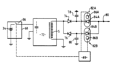
In Figure 4, the high voltage generator 72 is connected at its
low voltage input to s do battery supply 34 and a user-actuated
switch 36 forming part of a low voltage circuit G8. The high voltage
side of the secondary winding S of the step-up transformer
incorporated in the high voltage generator 72 produces a high voltage
in the form of an alternating pulse train (typically having a
frequency of the order of 20 Hz) which is coupled to a pair of
conventional high voltage diodes 74, 76 arranged in parallel but
biased oppositely. The alternating EMF' induced in the secondary
winding S is therefore rectified, diode 74 passing the positive going
cycles of the voltage and diode 76 passing the negative going cycles.
Capacitors 78, 80 are associated one with each diode 74, 76 to
eliminate voltage peaks and provide smoothing of the pulses.
Switching elements 82A, B control coupling of the generator voltage
to the output terminal 80 which in tuna is coupled to the nozzle in
any suitable fashion to apply high voltage to the liquid emerging a't
the nozzle outlet. Each switching element 82A, B comprises a high
voltage diode 84A, B and associated LED 86A, B and is arranged to
function in the manner previously described with reference to Figures
1 to 3.
Each diode 84A, B is connected in series and in back~to-back
relation with a respective one of the conventional diodes 74, 76.
Activation of the LED's 86A. B is controlled by control circuit 88 is
such a way that the diodes 84A, B are alternately and cyclically
rendered conductive in the reverse bias direction, control circuit 88
being activated in response to closure of user-actuated switch 36 (eg
_actuated in response to squeezing of a trigger associated with a hand
grip portion of the device). Control circuit 86 'is designed so that
diodes 84A, B are rendered conductive alternately with a frequency
appropriate to the effect to be achieved by means of the bipolar
output, eg shock suppression or spraying of insulating targets as
~~"''"~ WO 94!13063 2, ~ ~ ~ '~ ~ ~ PCT/GB93102443
-19_ 1
disclosed in EP-A-468736 and 468735. Thus, for example, the control
circuit 88 slay be aperable to control conduction of the diodes 84A
and 84B in such a way as to produce a bipolar output at terminal 80
of generally square wave form with a frequency of the order of up to
Hz, typically 1 to 2 Ftz.
It will be understood that the circuits shown diagramatically in
Figures 2 to 4 and the liquid supply will, in practice, be embodied
in a common housing so that the device is self-contained and
portable.
10 Referring now to Figure 5, in this embodiment high voltage
generator 100 teas its input side connected to low voltage do supply
circuit 101 and its output is intended to be coupled selectively to
one or more of a number of devices requiring a high output voltage.
Thus, in Figure 5 the generator 100 produces at the output terminal
102 thereof a unipolar voltage for application to three output
devices A, B and C which are connected to the output terminal 102 via
switching elements 104A, B and C each of which comprises a high
voltage diade 106A, B, C and LED's 108A, B, C and is arranged to
operate in the manner described hereinabove. The diodes 106A, B, C
are configured in reverse biased relation to the output voltage
generated by generator 100. The switching deices are controlled by
control circuit 110 which may be programmed or selectively operable
to supply current to any one or more of the LED's in order to render
the associated diode conducting in the reverse direction thereby
permitting the application of the voltage output of the generator to
the respective output device(s). In this way, the output devices A, B
and C can be operated in a pre-programmed sequence or any desired
manner. For instance, the control circuit 110 may be associated With
a number of user-operable 'switches or other means whereby the user
may select which of the output devices (such as electrostatic
spraying nozzles as described. herein) is to be operated. In response
to selection of a particular device by the user, the control circuit
110 may then activate the appropriate LED to permit supply of the
high voltage output from the generator to that device.
Referring now to Figure 6, the spray gun illustrated is intended
for hand-held use and is suitable for use in spraying relatively
viscous, low resistivity liquid formulations such as paints, at flow
WO 94/13063 PCT/GB93/02403
_ -20 s
rates of up to at least 4 cclmin. A typical formulation to be sprayed
has a viscosity of the order of 1 Poise and a resistivity of the
order of 5 x 10⁶ ohm.cm. The spray gun comprises a body member 202 ,
and a hand grip 204. The body member 202 is in the form of a tube of
insulating plastics material, eg a highly insulating material such as
polypropylene. At the end remote from the hand grip 204, the body . ,
member is provided with a collar 206 which is also composed of a
highly insulating materiel such as polypropylene and which is
screwthreadedly or other~rise releasably engaged with the body member
202 for quick release and access to the liquid container. The collar ."
206 secures a component 208 in position at the end of the body member
_ 202, the component 208 comprising a base 210 and an integral annular
shroud 212 which projects forwardly of the gun.
The base 210 has a central aperture through which a nozzle 214
projects, the rear end of the nozzle 214 being formed with flange 215
which seats against the rear face of the base 210. The~nozzle 214 is.
composed of a highly insulating material, such as a polyacetal (eg
"Delrin"), typically with a bulk resistivity of the order of
1015 ohm.cm: The body member 202 receives a replaceable cartridge 216
for delivering liquid to be sprayed to the nozzle 214. As the gun is .
required to deliver liquid at a flow rate of ep to at least 4 cc/min,
a positive feed of liquid to the nozzle 214 is needed and in this ,
embodiment of the invention is effected by the use a cartridge in the
form of a so-called barrier pack comprising a metal container 218
pressurised by a liquefied propellant, eg fluorocarbon 134A, and the
liquid to be sprayed is enclosed within a flexible metal foil sack
220 which separates the liquid from the propellant. The interior of
the sack 220 communicates with an axial passage 222 within the nozzle
vie 'a valve 224v which operates'ia a' similar manasr to the valve of a
conventional aerosol-type can in that displacement of the valve in
the rearward direction relative to the container 218 opens the valve
224 to permit positive liquid flow into the passage 222 (by virtue of
the pressurisation produced by the propellant). The passage 222
terminates at its forward erd in a reduced diameter bore forming the
cutlet of the nozzle. The forward extremity of the nozzle 214
terminates close to or at a plane containing the forward extremity of
the shroud 212.
~''T::n.
tr'e WO 94113063 ~ ~ ~~ ~ PC~'IGB93102403
2~.~~
_21'
Reaswardly of the cartridge 216, the body member 202
accommodates a high voltage generator 226 which is mounted in a
tubular carrier 228. The carrier 228 is mounted for limited sliding
movement serially of the body member 202. A tension spring 230 biases
the carrier 228 rearwardly. The high voltage generator 226 is of the
type which produces a pulsed autput and then rectifies and smooths it
to provide a high voltage DC output. A suitable form of generator 226
of this type is described in European Patent Application No. 163390,
The generator has a high voltage output pole 232 connected by lead
233 to a contact 234 secured to the carrier and arranged far
engagement with the rear end of the metal container 218. A second
output pole 235 of the generator is arranged to be connected to earth
via lead 236, resistor 238 and a conductive contact strip 240 secured
to the exterior surface of the hand grip 204 so that, when the gun is
held by the user, a path to earth is provided through the user. The
generator is powered by a low voltage DC supply comprising battery
pack 242 accommodated within the handgrip 204 and forming part of a
low voltage circuit including lead 236 coupled to earth tvia the
resistor 238 and the user) and a lead 244 connecting the battery pack
242 to the input side of the generator 226 vii a microswitch 246.
The val~re 224 is opened, in use, by relative movement between
the cartridge 216 and the body member 202, the nozzle 214 remaining
fixed relative to the body member. Movement to operate the valve 224
is applied to the cartridge 216 by movement of the generator/carrier
assembly, the latter being moved by operation of a trigger 248
associated with the handgrip 204 and which, when squeezed, pivots
lever 250 about its pivotal connection 252 thereby pivoting a further
lever 254 which is pivoted at 256 and is coupled to lever 250 by link
258. The lever 254 bears against the rear end of the carrier 228 so
that pivoting of the lever 254 is effective to displace the carrier
and hence the cartridge 216 forwardly thereby opening the valve 224.
Upon release of the trigger 248, the various components are restored
to their starting posit=ons as shown in Figure 6 by suitable biassing
means including spring 230. Squeezing of the trigger 248 is also
accompanied by movement of a linkage 260 which is coupled to the .
microswitch 246 so that trigger operation is accompanied by
~:,,
WO 94113063 PCT/G~93/0?,~03 ,'~"
214g4~
-22-
microswitch operation to supply low voltage power to the generator
226.
The high voltage produced by the generator, typically in ezcess
of 25 kV for a device designed to spray relatively viscous, low
resistivity liquids st flow rates of up to at least 4 cc/min (eg up
to 6 cc/m3n or even more), is coupled to the outlet of the nozzle 214
via contact 234, the metal container 218 and the liquid within the
passage 222 to provide an electric field between the nozzle tip and
the surroundings at earth potential. This electric field is
established with the aim of drawing the liquid emerging at the nozzle
outlet into a ligament which will break up into a divergent spray of
relatively uniformly-sized, electrically charged droplets suitable
for deposition as a uniform film. Because of the relatively viscaus
nature of the formulation to be sprayed (eg of the order of 1 Poise),
the diameter of the outlet has to be made relatively large (typically
at least 600 microns) in order to achieve flow rates up to at least
4 cc/min. Also, with relatively viscous materials, to achieve
satisfactory ligsrment formation (especially single, axially directed
ligament formation) at flow rates of this order, it is necessary to
operate at higher voltages than are necessary for lower viscosity
liquids since ligament Formation from viscous materials requires
increased electric field intensity.
For this reason, the generator 226 employed in the spray gun of
Figure 6 has an output voltage of 25 kV or greater as measured by
connecting the high voltage output of the generator to a Brandenburg
139I~ high voltage meter having an internal resistance of 30 Gigohm.
However, the use of voltages of this order would normally lead to
spurious spraying probably as s result of corona discharge effects
since the field intensity in the immediate vicinity of the nozzle
outlet may ezceed the breakdown potential of air. Such spurious
spraying may for instance result in highly polydisperse droplets in
the form of a mist of very fine droplets splitting off from the '
ligament and poorly divergent, paraxial streams of coarse droplets.
Satisfactory ligament formation and break np in the presence of
voltages of 25 kV or greater is achieved in the gun of Figure 6 by
provision of the component 208 and in particular the annular shroud
portion 212. The component 208' is composed of a semi-insulating
'- ~ WO 94/13063 ~ PCT/G~93/024I13 v
_2,3_
material (typically with a bulk resistivity up to 1011 -
1012 ohm.cm), eg ~Hytrel~ grade 4778 available from DuPont
Corporation, and is arranged with a rearwardly projecting annular
portion 262 thereof in contact with the metal container 218 so that
the voltage applied via the contact 234 is established at the forward
extremity of the shroud 212 and is of the same polarity as, and of
substantially the same magnitude as, the voltage produced st the
outlet of the nozzle 214. The annular portion 262 is trapped between
the forward end of the body member 202 and a flange 264 on collar 206
so that component 208 is fixed relative to the body member 202.
Operation of the trigger 248 leads to displacement of the container
218 relative to the component 208 but electrical continuity is
maintained by sliding contact between the leading end of the
container 218 and the inner periphery of the annular portion 262.
It will be understood that contact between the high voltage
generator and the shroud may be effected in ways other~than the
sliding contact arrangement shown; for instance the contact may be
made through a spring contact. Usually the contact arrangement will
be such as to ensure that a voltage substantially corresponding to
that established at the nozzle tip is developed on the shroud in
advance of, or substantially simultaneously, With the commencement of
spraying so that the shroud is immediately effective on commencement
of spraying.
By appropriate loeation of the forward extremity of the shroud
relative to the tip of the nozzle, the field intensity in the
immediate vicinity of the nozzle tip can be attenuated sufficiently
to produce formation of a single ligament which breaks up into
relatively uniform-sized droplets. The optimum position of the shroud
extremity can be readily~es'tabliahed by trial and error, ie by means
of a prototype version of the gun having an axially adjustable
shroud. In this way, the shroud can be adjusted forwardly from a
retracted position while observing the nature of the spray.
Initially, with the shroud retracted, the spurious spraying effects
referred to above are observed and as the shroud is moved forwardly a
position is reached where the spray quality improves markedly and
relatively uniform-sized droplets are obtained. Adjustment beyond
this point does not affect the quality of spraying initially but
WO 9~t/13063 ~ PC'TlGB93ID2403 ~F
-24-
tends to have a focusing effect. In practice,, where the voltage
established on the shroud extremity is of substantially the same
magnitude as that on the nozzle tip, we have found that the optimum
position tends be one in which the. tip of the nozzle more or less
coincides with a plane containing the forward extremity of the '
shroud; in a typical arrangement, using a shroud having an internal
diameter of 15 mm and an external diameter of 20 aan, the nozzle tip '
projects about 1 mm beyond this plane. Usually the arrangement will
be such that the angle between imaginary lines extending between the
forward extremity of the nozzle and diametrically opposite forward
extremities of the shroud is in the range 140 to 195°, more
preferably 150 to 180° (angles less than 180° corresponding to
the
nozzle forward extremity being forward of the shroud and angles
greater than 180° corresponding to the shroud being forward of the
nozzle forward extremity).
The marked difference in the nature of ligament break up can be
demonstrated by operating two nozzles under identical conditions with
the same liquid, one nozzle being operated without a shroud and the
other with a shroud located at an optimum position. A typical break
up regime in the case where no shroud is present involves the
production of a mist of very fine droplets a short distance ~rom the
nozzle outlet followed by break up of the central core of the
ligament into streams of poorly divergent coarse droplets. The spray
produced in this instanee is wholly unsuitable for the production of
a uniform film of the liquid (eg paint) on a surface to be sprayed.
In contrast, with a shroud located in an optimum position and
operating at substantially the same voltage as that prevailing at the
nozzle tip, the. ligament.was observed to travel a substantial
distance from the outlet of the nozzle before breaking up into
i
divergent streams of droplets having a narrow size distribution. The
production of a spray with droplets having a volume median diameter
of less than 100 microns was readily achievable when the nozzle was
t
operated with the shroud in an optimum position.
The presence of the metal container 218, coupled with the ,
relatively high voltage applied at the tip of the nozzle (ie usually
greater than 25 kV), can lead to a large build up of capacitively
stored charge during spraying with the possibility of the user
F
~.=:"~ WO 94113063 ~ !~ ~ ~ PCT/G893/02403
r.
_25-
experiencing an unpleasant electric shock if the user attempts to
access the interior of the device on cessation of spraying, eg for
the purpose of replacing the cartridge. This possibility is obviated
by the incorporation of means for discharging the capacitively stored
charge in response to cessation of spraying, such means conveniently
being arranged in the manner described in the embodiment of Figure 2
or 3.
The spray gun of Figure 6 is particularly suitable for spraying
liquids having viscosities between 0.5 and 10 Poise (especially 1 to
8 poise) and resistivities between 5 x 10⁵ and 5 x 10~ ohm. cm
(especially between 2 x10⁶ and 1 x 10~ ohm. cm) at spraying/flow
rates of up to at least 4 cc/min and more preferably up to 6 cc/min.
The diameter of the nozzle outlet and the voltage output of the
voltage generator 226 are selected according to the viscosity and
resistivity of the liquid to be sprayed. Typically the, nozzle outlet
will have a diameter of at least 600 microns in order to avoid
blockage by any particles suspended in the relatively viscous liquid
(eg. as in the case of a paint formulation) and to achieve the
desired spraying/flow rates without requiring undue application of
force to the trigger. The DC output voltage of the generator 226 will
A
typically be between 25 and 40 kV, more usually between 28 and 35 kV,
as measured by a Brandenburg 139D high voltage meter having an
internal resistance of 30 Gigohm. Although it is simpler to connect
the shroud 212 directly to the output of the generator 226 so that
the voltage established on the shroud is of substantially the same
magnitude as that prevailing at the tip of the nozzle, we do not
exclude the possibility of the shroud voltage being significantly
different from that of the nozzle tip; in this event, the difference
in voltages can be compensated for by appropriate positioning of the
shroud relative to the nozzle tip so as to secure the desired
divergent spray of droplets having a narrow size distribution. a
It will be understood that the spraying device described with ;
reference to Figure 6 may be additionally or alternatively modified
by incorporating electronic switching for other purposes described
herein, eg modification in accordance with the embodiment of Figure
4.
S
L