Note: Descriptions are shown in the official language in which they were submitted.
wo g "10630 2 ~ 6 !I PCrtAU93/00572 js-~ ~
!.` ;` ~ .
DATA FORMAl~ER I ;
TECHNICAL FIELD ~ -
' . ~
This invention relates to the general field of digital computing and more ` ~;
particularly to a method and apparatus for addressing a memory space in an
ordered manner to input and extract data structures. The invention may `
operate as part of a scalable array processing system.
BACKGROUND ART
The data formatter can be used as a member of a set of formatters which
provide data and instructions to a dataflow processor. An example of a
dataflow processor can be a systolic array of processing elements. The t -
subsystem formed by the controllers and the systolic array implements a high
performance tensor or matrix processing engine.
The formatter has two prima~ modes of operation. In the first mode it
generates addresses to read scalar operands from a memory space,
15 constructs a parallel set of operands comprising {instructiont data} 2-tuples,
and outputs the set in bit-serial form to an appropriate interface in
synchronism with other members of the set of formatters. In the second rnode, ;;
the formatter accepts, in synchronism with a nurnber of other data formatters,
all or part of a parallel data structure which is presented in bit-skewed bit~
20 serial form from an appropriate interface. When the formatter has stored in
internal buffers sufficient of tha parallcl data structure, it generates addresses :
to vvrite the stored data structure word sequentially into a memory space. ~ -
.:,
The parallel data structure can be considered as "wavefronts" which are ei~her
entered into the parallel interface or read f~om the interface. Wavefronts
25 consist of sets of ~instruction?data} 2-tuples which are bit-skewed between
adjacent processing elements.
DISCLOSURE OF THE INVENTI~N
It is an objsct of this invention to provide a data formatter adapted to providedata and instructions to a dataflow processor or at least to offer the pubiic a
30 useful alternative.
.:
21~18`161 F'E(~EIV~t~J '1 6~J~ 4' ~
2 ~`:
Therefore, according to one form of this invention, although this need not be
the only or indeed the broadest form, there is proposed a data formatter ' -
comprising:
a Bus Control means adapted to facilitate communication within the data
formatter and between the data formatter and externai memory means; ~ ~
an Address Generation means adapted to generate memory addresses for . ~ ~:
data fetch or storage; and , -
a Shift Register means adapted to provide local data storage and ~
communication with a dataflow processor. -
' :
In preference the data formatter is adapted to access at least one .:
predetermined region of the external memory means.
In preference the data formatter further includes an Instruction Fet~h means -
adapted to fetch and execute commands which determine the operation of the .
data formatter.
,.,~
In preference the. address generation means comprises a parallel datapath, a ~ -
local memory means adapted to store microprograms and a sequencer
means adapted to sequence the microprograms to generate addresses. :~.
.,,~,...
In preference the parallel datapath possesses an internal memory means
which stores parameters used by the microprograms.
20 In preference the shift register means comprises a number of serial-to-
parallel/parallel to-serial registers adapted to provide local storage of
wavefronts and communication with a dataflow processor. -~
In preference the data formatter is adapted to dete~t the presence of an IEEE ~;
infinity and effects an output dependant on such detection status. . ~i
,' ,
25 In one form the data formatter executes a linear sequence of commands.
In preference the address genera~ion rneans generates mem~ry addresses
fMm which data is read to load the registers of the shift register unit. ,:
Alternatively the address generation means generates memory addresses to
which data is written from the registers of the shif~ regis~er unit. '~
30 In a further form the invention can be said to reside in a method of formatting
~T~D S~T
~:PEAIAU
WO 94/10630 21 ~ I PCI'/AU93/00572 ~ .
,,`. ;; 3 ~ ::
data for provision to a dataflow p`rocessor including the steps of: j
(a) configuration wherein internal registers of the data formatter are initialised . - -
and loaded with informatior~ including instructions to be concatenated with ~
data during a wavefront execution phase; ;
5 (b) wavefront execution wherein addresses are generated, data is fet~hed
from the ~enerated addresses and instructions and data are concatenated to ¦
form ~instruction,data} 2-tuples which are output to the dataflow processor; `., ~.
and `
(c) termination wherein data formatting is terminated. I -
.
In preference steps (a) and (b) may be repeated an arbitrary number of times. ,-
ln preference the instructions are 5-bit opcod~s.
in preference the configuration phase can be performed under the control of a
bus control means by the fetching of commands from an external memory `:-
means or alternatively by explicit loading of parameters by a host processor.
BRIEF DESCRIPTION OF THE DRAWINGS
For a better understanding of this invention preferred embodiments will now
be described with reference to the attached dra~ings in which: ~-
FIG 1 is a schematic diagram of a data formatter;
FIG. 2 is a schematic diagram of a two-dimensional difference
engine; ~.
FIG. 3 is a C-code listing of an implementation of the algorithm
described in equation (1) for normal matrix storage and access;
FIG. 4 is a schematic diagram of the address generation for ~.
normal matrix accesses; ,. ~ -
FIG. 5 is a C-code listing of an implementation of the algorithm for
normal storaga and lower triangular rnatrix access;
FIG. 6 is a schematic diagram of the address generation for lower
triangular matrix accesses; ~;
W O 94/10630 2 1 ~1 Q~ ~l fi ~ 4 PCr/AU93/00572
FIG. 7 is a C-code listing of an implementation of the algorithm for
normal storage and upper triangular matrix access; ',
FIG. 8 is a schematic diagram of the addr sss generation for ~ -
upper triangular matrix accesses;
)--. .
FIG. 9 is a C-Code !isting of an implementation of the algorithm
for normal storage and strictly-upper triangular matrix access;
.
FIG. 10 is a schematic diagram of the address generation for
strictly upper triangular matrix accesses;
FIG. 11 is a summar~Ss of the interface signals between the formatter
1 n and both the host memory and the parallel data inter~ace;
. ,
FIG. 12 is a schematic diagram of a first embodiment of the
implementation of a data formatter in a system; and
,
FIG. 13 is a schematic diagram of a second embodiment of the
implementation of a data formatter in a system. `
8EST MODE FOR CARRYING OUT THE INVENTION ~-
.- ,. .
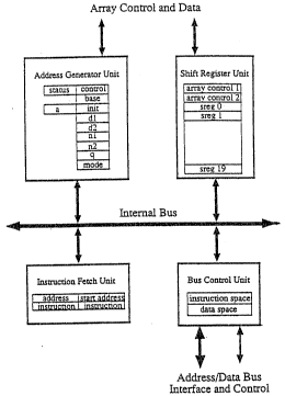
Referring row to the drawings in detail it can be seen from Fl(~i. t that in one - -~
embodiment the data formatter is comprised of four modules: the Bus Control
Unit; the Address Generatioris Unit; the Instruction Fetch Unit; and the Shi~t
Register Unit.
20 The bus control unit (BClij provides the control for the internal bus by which
functional units communicate betw~en themselves or with the external world. ~5
Requests for bus access are ordered in priority and serviced by the bus ~ :
control unit interface. External communications are also controlled by the bus ;~:~
controller. The external address and data bus and their associated pro~ocols .;
25 are interfaced to the internal bus in the bus control unit. External bus request
and bus ~r~nt are part o~ the interface, as is the multiplexing of address and ~ .
data. The internal registers within the various units are made availabie to the
externat bus by thé control unit so that they may be addressed as memory , ;:
mapped registers. A number o~ memory spaces are supported by the bus .
30 control unit. This allows the use ~ partitioned rnemory to enhance system
,~,...
WO 94/10630 21 !~ i PCI'/AU93/00~72
. 5 ~ -
speed. An example is a partitioned cache (described later) in which different ¦ :
matrix operands are stored in different partitions to improve the efficiency of
the cache. ¦
The Address Generation Unit (AGU) consists of a parallel datapath, ~
5 microprograrn ROM (Read Only Memory) and a microprogramed sequencer.
The address for either source or destination data are computed by the AGU i .
and passed to the bus control unit to be used in data reads and writes. A
number of microprograms are held in tl~e microprogram ROM which enable
thne AGU to perform a range of different addressing modes. `
The Shift Register Unit (SRU) contains ?0 serial-to-parallel/parallel-to-serial ~ ;
registers. These shift registers constitute the local storage for structured data
which is input either from the sequential memory accesses of the address
generator unit when reading structured operands from memory, or from the
parallel bit-serial inputs prior to writing a result back to memory. ~-
The formatter is controlled by the host either directly or indirectly. In the direct ~ :
control case, the host writes configuration data directly into the registers of the
formatter, and then initiates the device by writing to a control register.
Determination of the completion of a formatter sequence is done by polling a
status register.
Indirect control of the formatter is effected by a program resident in an
accessible memory space which is fetched and executed by an instruction
fetch unit in the formattèr. The initiation of program execution is carried out by
writing the address of a program into th~ Program Address register. Fetched .
commands load internal registers which are used to specify the parameters of
the data structures to be fetched from or stored to a specified memory space. I -
The command set for the formatter is given in table 1, where the following
conventions are used ~
. . :~.
< dest > The name of a valid destination register.
~ data > A 32-bit immediate word.
30 ~ short data ~ A signed (2's complement) 23-bit immediate data word. ~ ~ -
~ mode ~ The name of an AGU program mode. ~ ~
`:
WO 94/1Q630 PCI`/AU93/00572 ~s ;i;
Label I Code I Descri tion ¦ S ntax 1,
_ _ _c -P - - Y ~ .
HALT 000 tlalt and interrupt HALT ( ) __
LOAD 001 Load immediate data LOAD (<dest>,cdata~) t
. _._ _ _ _ ~ _~ J :-, :`.
LOADQ 010 Load quick immediate data LOADQ (<dest>,<short qata>) ~ ~ ~
_ . _ ~ , . . ~
WAVE 01 1 Execute AGU ~roqram WAVE (<mode>)
. _ ___ ~ . ~ ~.
NOP 111 No o~eration NOP ~ ) ;
_. ~ , _ . ,:',.
TABLE 1
As a matrix example, parameters which specify the data structure include the
length of a data vector, the starting address in memory, the number of rows
and columns of the matrix and the linear spacing between matrix elements.
5 Additional commands are used to initiate the transfer of parallel data in
wavefronts, and to interrupt a host processor. No conditional or branch
statements are present in the command set, and the formatter executes a
linear sequence of commands until a halt command is executed. Branching
commands can be incorporated into the command set if desired. This
10 command causes the formatter to activate an interrupt signal and go into a
wait state until a new program start address is written to the Program Address
register. The typical program consists of the following sequence of phases:
configuration; wavefront execution; termination. ;;~
~ '"''`.''`,".
In the configuration phase the internal registers of the formatters are
15 initialised, together with the loading of the instructions which are to be
concatenated with the data during the output of a wavefront. `
,-:
In the wavefront execution phase data is fetched and stored in the internai ;
shift registers, instructions are appended and the {instruction,data} 2-tuples
are output serially as wavefronts after the set of formatters has synchronised. ; ,
The address generator unit is used either to generate memory addresses from
which wavefront data is read to load the shift registers, or to generate memory
addresses to which wavefront data in the shift registers is written. Two 5-bit
opcodes are stored in the forrnatter for appending to the data during output.
Tho first is output with the first data wavefront and the secon~ is output during
all subsequent wave~ronts of a given data stru~ture. ;`
~ .,
In the termination phase command fetching is terminated by a HALT
command, and an interrupt signal is asserted.
,~,
~ ` ~'Cr/AU93/00572
WO 94/1~630
r ~` ~
Additional configuration and wavefront execution phases may occur before a t` `
termination command is executed. The length of a formatter program is ¦ -limited only by the address space. I ; `
Table 2 is a read/write register map of the formatter. Fi~teen registers are used
for configuration and control information, and twenty r~gisters are used in the ,~
shift register unit for the parallel loading and storing of structure data.
: `
The instruction fetch unit uses registers O and 1 as a program counter and a
command holding register respectively. The program start address is initially
written to register 0 and subsequent reads return the address of the next
1 O command to be fetched.
¦ 51 ¦ Data register 1
_ _
33 ~
~32 ~ .
. _. . ,: ::
_AGU mode _ _
14 Modulo -
_ _ . : ~
13 Wavefront count ~
. _. . . .
12 Element count ~
_ _ _ _ _ ` .:
1 t Wavefront spacing
~ .-
1 O Element spacing - ~ ~
~ , ,. :~ :
9 Initial offseVElement address :
_ ~ :-
8 Base Address ~ ;
7 Arrav control 2 : -~
~ .
6 ~ .
4 Status/Control
, ~
3 _~Data Space _ `.-.:
2 _Instructio~ace
1 _ _ Instruction _
O _ ~dress
TABLE 2
WO94/10630 21 ~ 5 PCI'/AU93/00572 ~ ~
}
Registers 2 and 3 contain 8-bit AND and OR masks for the command space
and 8-bit AND and OR masks for the data space. They are used by the Bus :
Control Unit to calculate and output an 8-bit descriptor for both data and
command addresses.
~ .
Register 5 is a 3-bit status and control register providing information regarding
the following:
Infinity Detected: an infinity has been detected in a value which has been
entered into a shift register. Setting this register bit clears the Infinity Detected
bit. -.
Interrupt: the formatter is asserting an interrupt. Setting this register bit ciears ~`
the interrupt.
AGU Busy: the address generator is executing a program. Setting this ~ -
register bit starts the AGU if the parameters have been written into the AGU.
Registers 6 and 7 are two array control registers used to define the way in
which the formatter communicates with the parallel interface. The first register ;
specifies information concerning the properties of the first wavefront
transmitted to the interface. In particuiar these elements are:
inter-wavefront gap: a variable wait perind between wavefronts.
element iength: the number of bits in each 2-tuple passed to the interface. `
wavefront type: a 2-bit field which identifies the type of wavefront.
negate: a flag which causes the sign bit of all operands processed to be
reversed, so negating the operand. -
opcode: a 5-bit field which is output as one element of the operand 2-tuples
transmitted to the interface.
The set of opcode~ and their functions are set out below: ;
Instruction Bit No. Function
ADD 4 Floating point add
LDR 3Convert result to IEEE format and load O/P register
HAD 2Enable resuit unloading only if diagonal flag sat ~ `
SDE 1Set DIAGONAL flag if accumulator contents are non-zero : -
CLR O Clear accumulator priorto computation
The second contro! r gistsr contains an identical set of parameters to the first,
with the exception of the negate flag which is specified by the first register.
'
WO 94/10630 21~ PCI`/AU93/00572
''``"``; 9 ~':'.'''
The parameters held in this second control register are used to specify the
properties of all wavefronts subsequent to the first.
The address generator unit (AGU) consists of a general purpose arithmetic
datapath and two 20-bit increment/decrement datapaths. Control of the
datapaths is effected by programs resident in a microcode ROM internal to the 1~ -
AGU. Microprograms for a number of different matrix addressing algorithms t~
are present in the ROM. These programs are initiated either by a Wave
command, or the setting of the AGU bit of the status and control register.
The AGU utilizes registers 8 to 15 of the registers lis~ed in Table 2. The eight destina~ion registers are loaded either by host writes to the memo~y-mapped
registers, or by the LOAD or LOADQ commands. The only readable register is
9, which contains the current address generated by the AGU. -
The address generated by the AGU is dependent upon the set of parameters
{Argurnent type, Storage mode, Access mode}. Taking these parameters in
order:
Argument ~ype: The argument type can be one of three; C)perand, Result and
Hadamard Result. Operand programs are used to access operand matrices to
be output to the parallel interface. Result programs are used for storing the
data structures input from the parallel interface when the structures are
generated from a conventional matrix multiplication. Hadamard Result
programs are used when the structure input from the parallel interface has ~:
been generated with an elsment-wise operation. They cause additional : -
synchronisa~ion protocols to be observed betweerl all data formatters in a
system. ~ `
Storage mode: The storage mode of matrix operands have been defined as
one of the set {Normal, Triangular, No storage }. For matrix operands stored
normaliy, every element in the matrix is written into a memory location,
whereas for triangular operands the zero elements are not writ~en ~o ~he
memo.~, so allowing packed storage techniques to be used. ~,
The access mode of a matrix structure can be arl ~lement of the set {Normalt -
Upper triangle, Strictly upper triangle, Lower triangle, no access}. Access ~or
each is described as follows:
0 94/10630 2 ~ 3 ~16 i~ 10 pc~/Aus3/oos72
r;
.~ .
Normal: Addresses are generated for all elements, and all elements are
accessed in host memory.
Upper triangle: Only elements on the diagonal and in the upper triangle are
accessed in host memory. Other elements are defined to be zero, and~so are
5 neither read nor written.
'' '~
Strictly upper triangle: Only elements above the diagona! are access~d in
host memory. Other elements are defined to be zero, and so are neither read - ;-
nor written.
~ . .
Lower triangle: As for the Upper mode, only elements on the diagonal and in
10 the lower triangle are accessed in host memory. Other elements are defined
to be zero, and so are neither read nor written. .
No access: No elements are written to host memory.
A general approach to matrix addressing is to use a second order difference
engine, implemented with a modulo arithmetic capability. The following
expression is irnplemented in hardware: '`
"
a = base_address + ~init + n1d1 ~ n2d2) mod q (1)
'.',.'
This maps an element of an arbitrary matrix ~XI, stored at address a in a linearaddress space starting at base_address, onto the ~n1, n2) element of a two- .
dimensional address space. The parameters of the right hand side of this ~;
expression are loaded into the registers of the datapath in the address '- -
generator. ~-
To address sequentially a!l elements of the matrix, n~ and n2 are indexed
through their respective ranges (the dimension of the matrix). This is carried
out using the difference engine principle shown in FIG. 2. For the first row of
~he matrix, addresses are formed by n1 - 1 accumulations of the first differeneevalue d1, where each opsration is carried out modulo q. The address of the ~ `
~irst element of the second row is computed by accumutating the second
difference d2 modulo q, and the remaining addresses of the matrix elements
are computed by repeating this procedure. Prirne-radix mappings can be
implem-nted directlywith this ~echnique.
.
,
WO 94~1û630 21 ~1 ~ q s, ;~ PCI/AU93/00572
To enable thQ addressing of non-rectangular data structures, the dimensions ~ -
{nj} are variable. By linearly decreasing one of the two dimenslons in a matrix ,.
it is possible to generate addresses for a triangular region of the matrix. The
symbol <.> in FiG. 2 represents evaluation modulo q.
' .~'.
By non-linearly non monotonically changing one or more dimensions of a n-
dimensional matrix one can generate non-rectangular addresses for data
structures.
FIG. 3 is a C-code listing modelling the normal storage, normal access matrix
address generation algorithm derived from equation ~1), and FIG. 4 is a
schematic representation of the method of generation of the addresses.
An example of the execution of th0 algorithm can be shown for a simple 3 x 4
matrix stored in normal order. The address sequence generated using the
arguments {0,0,1t1,4,3,12} is
~0 1 2 3
4 5 6 7 ~
~8 9 ~L0 11 .:.
Note that the access () function models the accessing of data in memory. If the
matrix was of type Operand, the access (a, sreg~ call would fetch the contents
of memory at address a and write the data into the shift register number sreg.
If the matrix was of type Result, the contents of shift register number sreg ;-~
would be written into rnemory location a. -~
FIG. 5 is a C-code listing modelling the normal storage, lower access matrix
address generation aigorithm derived from equation t1), and FIG. 6 is a ! ~
schematic repr~sentation of the method of generation of the addresses. -~-
An example of the execution of the algorithm can be shown for a simple 4 x 4
matrix stored in normal order. The address sequence generated using the
arguments {0,0,1,4,1,4,16} is ~;
O
4 5
8 9 10
2 13 14 lS
:
W0 94/10630 21'~ 3 ~ 12 PC~/AU93/00~7Z
s, ,. ~ :
FIG. 7 is a C-code listing modelling the normal storage, upper access matrix 3address generation algorithm derived from equation (1), and FIG. 8 is a
schernatic representation of the method of generation of the addresses. -~
An example of the execution of the algorithm can be shown for a simple 4 x 4
5 matrix stored in normal order. The address sequence generated using the
arguments {0,0,1,5,4,4,16} is s
0 1 2 3 ,~
5 6 7 . .
10 11 . .
. . ~
.,",'
FIG. 9 is a C-code listing modelling the normal storage, strictly-upper access
rnatrix address generation algorithm derived from equation (1), and FIG. 10 is
10 a schematic representation of the method of generation of the addresses.
An example of the execution of the algorithm can be shown for a simple 4 x 4 --
matrix stored in normal order. The address sequence generated using the
arguments ~0,1,1,5,3,3,16} is
1 2 3~ ;
llJ ~
~`
-;...
The formatter comrnunicates with the host system memory via a multiplexed
address/data bus and assoeiated bus control signals The bus is 32-bits wide.
Multiple formatters can be connected to a common system bus with the use of ~ -
an asynchronous bus-requcsVbus-grant protocol. One such interface is
shown in FIG. t 1.
FIG. 12 shows a system diagram in which form~ers are used to input two
parallel data structur~s into a systolic processor array from a global system A
bus, and also to accept the output of the array and write the output back onto
the system bus.
. ,~
In a second embodirnent shown in FIG. 13 the invention has been `~
25 impiemented in a systern hosted by a Sun SPARCstation. The matrix
processor is interfaced to the Sun SPARCstation ~ia the SBus. This
WO 94/10630 2 1 ~ 8 ~ fi ~-1 PCI'/AU93/00572
r I 1 3
arrangement is convenient since it aliows the SCAP hardware to operate
using virtual addressing, with virhlal to physical translation being performed
by the SBus controller in the SPARCstation. The host processor and the
matrix processor therefore share the same data space, so both can interact ¦'
with the matrix data directly. This approach does however have its own ! ::
disadvantages, the most critical being the fact that the data transfer rate across
the SBus tends to be quite low (only 1.5 to 3.85 Mwords per second) due to ':
the overheads of address translation.
To compensate for this low data rate, the matrix processor also includes a
cache memory subsystem. The cache supports burst mode data transfers
across the SBus on cache misses and can also be used to hold frequently
used operand matrices (such as coefficient matrices in transform applications) :
and to store temporary or intermediate results.
A novel cache partitioning scheme has been implPmented. The technique
allows the cache to be dynamically divided into a number of regions that are
guaranteed not to interact thereby ensuring that fetches for one matrix - -~
operand do not interfere with fetches for the other. The data controllers
determine how the cache is partitioned on a per-operand/result basis (it is
also possible to assign a cache partition to the command streams) by issuing
an 8-bit space address along with each address generated. Each bit of the
space address can be set or cleared, or can take on the value of one of the
generated address bits. In our system implementation, three bits of this space
address are used to control non-cached accesses, temporary matrix accesses ~
and temporary matrix initialization. Four bits are used to partition the cache ~ ~-
into up-to 16 independent regions. Use of the temporary matrix control bits of
the space address altows temporary result matrices to be stored entirely within
the cache without being written out to the host. in fact, such matrices are ,-;
entirely invisible to the host processor. The maximum data throughput Ti~
obtainable using the cache is 12.5 Mwords/second.
.
The data formatter chip was designed using a generic 1.2 micron double layer ~;
metal CMOS process rule-set and were retargetted for fabrication using
Hewlett Packard's 1.0 micron HP34 process using a gate shrink. The ~.
processing element chip is described as part of a second embodiment in a co- i
pending app~ication number PL~697 entitled SYSTOLIC DIMENSIONLESS i
ARRAY. ' ; ~.
WO 94/10630 , PCI/AU93/00572
3 ~ 14
The data formatter chip was designed using a mixture of full custom and
standard cell design styles. Data formatter chips are used to fetch operands
from matrix data structures held in the host memory system, and to store
results back into the host memory and/or cache.
The data formatter chips implernent matrix addressing~ They access the t "~
elements of the matrix using information frorn a matrix descriptor that specifies
the base address of the matrix, element spacing and row/column spacing, etc. .
The same chip can be used as either an operand data formatter or a result
data formatter. A number of addressing modes have been implemented to ~ n
support conventional matrix multiplication, element-wise operations and ~.
certain triangular access modes. Constant and circulant matrices can be
stored and accessed efficiently. Both real and complex matrices are ~:
supported. Matrix transposition, negation, and subrnatrix evaluation can be
performed by the data controllers, as can more complex mappings or
permutations of the matrix elements (e.g., prime factor mappings).
" :'`
The data formatters fetch one operand for each processing element along the
two edges X and Y of the array, and then transmit the data to the array as a `~ -
block known as an operand wavefront. The operand wavefront also includes -
an instruction opcode that is transmitted to the array along with the data. The ~; ~
opcode specifies to the processing elements what type of computation is to be ~1 `
performed (e.g. multiply/accumulate, element-wise addition, clear
accumulator, etc). Bit-serial communication to the processing element array is
used, with a one clock cycle pipeline delay between each processing element
in each dimension of the array. This approach approximates broadcast
operation, but caters for arbitrary expansion.
Result wavefronts are rea~ back from the processing element array using a
similartirning scheme.
Data formatter chips have the ability to fetch and execute their own command ;
streams. This minimi7es host int~rvention and thereby improves sy~tem
pe~formance. Data formatter programs describe the matrices involved in the i-
computation and specify the methods by which the matrix data is to be
accessed as well as the operation(s) to be computed by the array. A data ~`
formatter program can be as simple as a single matrix multipiication or as
complex as an entire application. When all data formatters have finished
executing their programs, an interrupt is issued to the host processor to signal ':
~. .
WC) 94/10630 21 4 ~ PCr/AU93/00572 ~ ~ `
.. , . l`"
thatthe results are available.
Each data formatter chip can provide data to or receive data from up to 20
processing elements along the edges of the array. Therefore, a system
containing up to 400 processing elements (20 PE chips) can be contr~lled
with just 3 data formatter chips: one for each of the X and Y operand data I ~ `
streams, and one for the result data stream R. I
Data formatter chips can be cascaded to support arb`itrarily large processing
element arrays. A system containing up to 1600 processing elements (80 PE
chips) requires 6 data formatters, while a 3600 PE array (180 chips) requires 9 ` -
data formatter chips. Table 3 shows the statistics associated with one
embodiment of the data formatter chip.
Number of Transistors 130 000
Die Size (Pad to Pad) _ 6.21mm x 7.83mm _
Transistor Density _ _700 T/sq mm ;~
Power Dissipation_ ~ .0 Watts _ _ `~;
Package _ 1 20PGA __
Maximum Internal Instruction 25 MHz
Frequency _ _ _
Address Generation Rate _ 6.25 Mwords/sec _ _
TABLE 3
The performance attained by the apparatus of the second embodiment for a , ~ `~
15 range of applications is shown in Table 4.
i~ '
. "'
.
. .
.. .
WO 94/10630 PCl/AU93/00572
,.. S `.~ ~ ~ 1 6
_ ~ ~ ' ,''
, .~ _ _ :'
3450 point 1 D Fourier transform 20 msec 130 MFLOPS :
usina 2D factorization ~ ~ -
~ _ _ _ ~1, `,
2D Fourier Transform of 380380 1385 msec 66 MFLOPS , I ;
point image ~
4000tap FIR Filter 35 msec per 1000 210 MFLOPS , .
data samples
_ _ . , ~
1Oth order Matrix polynomial 136 msec 114 MFLOPS
evaluation of 60 x 60 complex .~ ~:
matrix . i :-
QR factorization of ~9 x 60 M trix_ 561 msec 87 MFLOPS ;
TABLE 4 .;`.;
'~`
' ~
:, ,
` ~
'~
:
..... .. .... ~.. ... , ~, . . ... .. .