Note: Descriptions are shown in the official language in which they were submitted.
CA 02148533 2004-05-31
DIGITAL SIGNAL RECORDING APPARATUS WITH FANS FOR DETECTING_
AN ID SIGNAL AND CONTROLLING THE NU1~ER OF SIGNAL SAMPLES
~3ACKGROUND OF THE INVENTION
Field of the Invention
The present invention relates to a digital
signal recording apparatus for recording for example an
audio PCM signal to a magnetic recording medium through
a rotating magnetic head.
Description of the 3elated Art
When an audio PCM signal is recorded as a
sound signal by a digital signal recording apparatus,
if the ratio of the sampling frequency fs~~and the
internal inter7.eave reference signal frequency is not an
integer, an image signal and audio PCM signal are
synchronized so that they are properly recorded and
reproduced. It is assumed that the audio PCM signal. is
interleaved in a frame and the sampling frequency fs is
48 kHz. In this case, the frame frequency is 29.97 Hz.
Thus the ratio of these signals is represented as
follows.
48000 /29.97 = 1601.6 (11
Consequently, the ratio ~of these signals is not an
integer.
As an integer that is closest to the
quotient, it is assumed that 1602 is designated the
standard number of samples of data recorded at one.
interleave region.. In addition, two numbers of samples
1
numbers for example 1592 and 1612 are designated as a
smaller number and a larger number of the standard
number of samples, respectively. The number of samples
of the audio PCM signal to be recorded is measured.
The cumulative value of the number of samples and the
cumulative value of one selected from the designated
numbers of sampled are compared in frame frequencies.
When the cumulative value of the number of
samples is larger than the cumulative value of the
designated value, 1612 is selected. In contrast, when
the cumulative value of the number of samples is smaller
than the cumulative value of the designated value, 1592
is selected. The selected number of samples are
recorded to a recording medium as data for one frame.
In addition, an identification signal that represents
the number of samples of record data is recorded.
When the sampling frequency fs is 32 kHz, the
ratio of the sampling frequency and the frame frequency
is represented as follows.
32000 / 29.97 = 1067.7 (2)
Thus, the ratio of these frequencies is not an integer.
It is assumed that an integer 1068 that is closest to
the quotient is designated the standard number of
samples of data recorded at one interleave region.
When two sample numbers 1058 and 1078 are designated as
2
a lower number and a larger number of the standard
number of samples, respectively, the above-described
sampling frequency fs can be recorded in a similar
manner to the case of 48 kHz.
In the above description, it is assumed that
two numbers of samples are designated as a lower number
and a larger number of the standard number of samples.
However, it should be noted that the numbers of sample
numbers may be two or more. For example, when the
numbers of samples is four, if the sampling frequency
fs is 48 kHz, 1622, 1612, 1592, and 1582 may be
designated.
When the sampling frequency fs is 32 kHz, four
numbers of samples 1088, 1078, 1058, and 1048 may be
designated. When more numbers of samples are
designated, the above described cumulative values can
be more precisely controlled.
Thus, even if the number of samples for one
frame is an integer, the number of samples that is
close to the above-described standard number of samples
is averagely recorded. Thus, dis-synchronization
between the image signal and the audio PCM signal can be
prevented. When signals are reproduced, the
identification signal extracted from the reproduction
signal is cumulated. Thereafter, the phase of the
cumulative value is compared with the phase of the
cumulative value of the sampling clock formed in PLL
3
CA 02148533 2004-05-31
(Phase Locked Loop). The compared output is supplied
to a~VCO of the PLL. Thus, as with the casein the
record mode, th~~ relation between the interleave
reference signal and the sampling clock is maintained
in the reproducing state, thereby correctly reproducing
digital signals.
It is noted that the prior art related to the above-
mentioned technique is disclosed in European Patent No.
0,561,281 filing date March 11, 1993, corresponding the US
Application.
When t:he sampling frequency fs and the number
of quantizing bats Qu are decreased, the number of
channels that can be independently recorded can be
increased. Now,, it is assumed that half the channels
are after-recorded. When the sampling frequency fs is
48 kHz, the number of quantizing bits is 16, and the
number of channels is 2, the transmission rate of
digital data on two channels is. represented as follows.
48000 x 16 x 2 = 1.56 (Mbps) (3)
When the sampling frequency fs is 32 kHz, the
number of quantizing bits Qu is 12, and the number of
channels is 4, the transmission rate of digital data is
represented as i:ollows .
4
32000 x 12 x 4 = 1.536 (Mbps) (4)
Thus, these transmission rates in the above-described
two cases are the same.
In other words, when the sampling frequency
fs is 32 kHz, the number of quantizing bits Qu is 12,
and the number of channels is 4, the remaining two
channels rather than two channels that have been
recorded can be used for after-recording.
However, when the after-recording is
performed, if the above-described numbers of samples
are controlled independent from those for two channels
that have been recorded, different identification
signals are used. Thus, to reproduce signals, two sets
of signal reproducing portions are required.
Therefore, an object of the present invention
is to provide a digital signal recording apparatus that
can perform after-recording for a digital signal in
which the ratio of the sampling frequency fs of a
digital information signal to be recorded and the
frequency of the internal interleave reference signal
is not an integer without need to use a complicated
signal reproducing portion.
SUMMARY OF THE INVENTION
A digital signal recording apparatus having a
non-integer relation between a sampling frequency of a
2~~~5~~
digital information signal to be recorded and an inner
interleave reference signal frequency, comprising a
sample number controlling means for controlling the
number of samples at an interleave region so that the
number of samples of data that has been recorded
becomes equal to the number of samples of an
information signal, when the after-recording is
performed for the recording medium on which data has
been recorded, and a recording means for pre-detecting
an ID signal that identifies the number of samples at
the interleave region from the recording medium and
recording the ID signal to the recording medium along
with the information signal that is after-recorded.
When after-recording is performed, an
identification signal that represents the number of
samples of a data portion that is not after-recorded is
pre-detected. Corresponding to the identification
signal, the sampling frequency fs of an information
signal to be after-recorded is controlled. Thus, the
number of samples that is equal to the number of
samples of the data portion that is not after-recorded
is recorded. Consequently, the reproduction signal
processing portion can perform signal process with only
one sampling clock control operation regardless of
whether or not the after-recording is performed.
In addition, an ID signal for a pre-recorded
data portion is detected. The same ID signal can be
6
recorded in an after-record region along with an
information signal to be after-recorded.
According to the present invention, the E/D
ID is detected from the ID region of the data portion
that has been recorded. The same E/D ID as the
detected E/D ID can be recorded in the after-record
region along with an information signal to be after-
recorded.
In addition, the fs clock generating PLL
portion and the reproduction signal processing portion
(for example, an identification signal detecting portion
that represents the number of samples) can be
constructed as one system.
Moreover, since the data sampling frequency
controlling portion used for after-recording is
constructed in common with the fs clock generating PLL
portion, the apparatus can be simply constructed at low
cost.
Furthermore, according to the present
invention, although an audio PCM signal is used, still
image data such as digital video can be recorded.
The above, and other, objects, features and
advantage of the present invention will become readily
apparent from the following detailed description
thereof which is to be read in connection with the
accompanying drawings.
7
BRIEF DESCRIPTION OF THE DRAWINGS
Fig. 1 is a schematic diagram showing an
example of the structure of a block according to the
present invention;
Fig. 2 is a schematic diagram showing an
example of the structure of a track according to the
present invention;
Figs. 3A and 3B are schematic diagrams showing
an example of the structure of a frame according to the
present invention;
Fig. 4 is a schematic diagram showing an
example of interleaving on a track according to the
present invention;
Fig. 5 is a schematic diagram showing an
example of interleaving among tracks;
Fig. 6 is a schematic diagram showing an
example of a record region of each signal of a magnetic
tape pattern according to the present invention;
Figs. 7A and 7B are flow charts showing an
example of a signal process of a digital signal
recording apparatus according to the present invention;
Fig. 8 is a block diagram showing a digital
signal recording apparatus according to an embodiment
of the present invention;
Fig. 9 is a block diagram showing a record
signal process according to an embodiment of the
present invention; and
8
2~4~~~
Fig. 10 is a block diagram showing a sampling
clock controlling portion according to an embodiment of
the present invention.
DETAILED DESCRIPTION OF THE PREFERRED EMBODIMENTS
Next, with reference to the accompanying
drawings, an embodiment of the present invention will be
described. The description will be made in the
following order.
(1)Example of structure of block
(2)Example of structure of track
(3)Example of structure of frame
(4)Example of interleaving on track
(5)Example of interleave
among tracks
(6) Record regions of signals on magnetic tape
according to present invention
(7) Flow chart of signal process of digital signal
recording apparatus according to present invention
(8) Example of entire block construction of
digital signal recording apparatus according to present
invention
(9) Example of block construction of recording
portion
(10) Example of block construction of sampling
clock controlling portion
(1) Example of structure of block
9
2~~~~
Fig. 1 is a conceptual schematic diagram
showing an example of the structure of one block of
record data. One block is composed of a header
portion, a main data portion, and a C1 parity portion.
The header portion is positioned at the beginning of
the block and composed of a block sync (Sync)(two
bytes), header IDs (IDO and ID2)(two bytes), and a
header ID parity (one byte). Thus, the header portion
is composed of a total of five bytes. A track ID
number (1 to 10) is written to the low order four bits
of the header IDO. A block ID number (1 to 14) is
written to the low order four bits of the header ID1.
The main data portion (hereinafter referred
to as data portion) is composed of 78 bytes. Data and
C2 parity are written to the data portion. At the
beginning of the data portion, there is a region in
which an ID signal that identifies whether data
recorded in a frame portion is E data frame (excess
data frame) or D data frame (diminished data frame).
The C1 parity portion is composed of eight bytes.
Thus, one block is composed of 91 bytes.
(2) Example of structure of track
Fig. 2 is a conceptual schematic diagram
showing an example of the structure of data of one
track. One track is composed of a first data portion
(five blocks), a C2 parity portion (four blocks), and a
second data portion (five blocks). Thus, one track is
~~~~'~ 5~
composed of a total of 14 blocks.
Even number data on L and R channels are
positiored in the data portion at addresses BA1 to 5
(hereinafter, these data are referred to as even number
sequence) . Odd number data on L and R channels are
positioned in the data portion at addresses BA10 to 14
(hereinafter, there data are referred to as odd number
sequence). A parity that is interleaved in the
direction of block addresses BA is placed in position
of the C2 parity portion at addresses BA6 to 9.
(3) Example of structure of frame
Figs. 3A and 3B are conceptual schematic
diagrams showing an example of the structure of data of
one frame. As shown in Fig. 3A, one frame is composed
of 10 tracks. Signals on L channel are recorded on
tracks TR1 to 5. Signals on R channel are recorded on
tracks TR6 to 10. As shown in Fig. 3B, these tracks are
recorded on a magnetic tape.
(4) Example of interleaving on track
Fig. 4 is a conceptual schematic diagram
showing an example of interleaving of data recorded on
a track. For simplicity, only track TR1 will be
described. In Fig. 4, five blocks of the first data
portion and five blocks of the second data portion are
shown. Four blocks of the C2 parity portion are
omitted. As described above, data on L channel is
written to track TR1. The regions surrounded by solid
11
214'8~~3
lines represent ID regions. In each of the ID regions,
E/D ID, sampling frequency fs, number of quantizing bit
Qu, and so forth are written.
In Fig. 4, the vertical direction and the
horizontal direction are defined as symbol address SA
direction and block address BA direction, respectively.
With respect to data L0, the data sequence in the
symbol address SA direction is L0, L50, L100, L150,
L200, ..., and so on. Thus, the interleave length in
the symbol address SA direction is 50 samples.
Likewise, with respect to data L0, the data
sequence in the block address BA direction is L0, L10,
L20, L30, L40, ..., and so on. Thus, the interleave
length in the block address BA direction is 10 samples.
The interleave lengths in the symbol address SA
direction and in the block address BA direction are the
same as those of data of even number sequence, odd
number sequence, and other track TR data.
Now, as described above, it is assumed that
the standard number of samples is 1602 and that the
numbers of samples of IDs (fl, f2) of two bits are
represented as follows.
(0,0) 1582 (number of D2 data)
.
(0,1) 1592 (number of D1 data)
.
(1,0) 1612 (number of E1 data)
.
(1,1) 1622 (number of E2 data)
.
12
~1~~~~~
When the frequency of the reference signal
that is recorded is the same as the frequency of the
reference signal that is reproduced, it is not
necessary to designate the number of samples other than
the standard number of samples. However, when a
digital interface input is considered, the sampling
frequency may deviate for around ~ 1000 ppm. Thus, the
number of samples should be designated so that it can
absorb such deviation. When the sampling frequency fs
is 48 kHz, the deviation of ~ 1000 ppm becomes 48.048
kHz (+1000 ppm) to 47.952 kHz (-1000 ppm). Thus, the
number of samples should be designated with proper
tolerance.
Now, it is assumed that the standard number of
samples is 1602, the number of E data is 1612, and the
number of D data is 1592. In this case, when the
frequency of the reference signal is 29.97 Hz, the
sampling frequency fs of the number of E data is
represented as follows.
29.97 (Hz) x 1612 = 48.31 (kHz) > 48.048 (kHz).
The sampling frequency fs of the number of D
data is represented as follows.
29.97 (Hz) x 1592 = 47.71 (kHz) < 47.952 (kHz).
13
Thus, the deviation of ~ 1000 ppm can be
absorbed.
Individual data are interleaved and written to
corresponding tracks. At this point, in non-data
regions, null data (OOH) is written. Regions at BA5 and
SA7 and at BA14 and SA7, an ID signal generated by an
E/D ID generating circuit (that will be described
later) is written.
(5.) Example of interleaving among tracks
Fig. 5 is a conceptual view showing an
example of interleaving of data recorded among tracks.
With respect to data LO of the even number sequence on
track TR1, the data sequence on tracks is L0, L2, L4,
L6, L8, ..., and so on. Thus, the interleave length
between each track is two samples.
With respect to data L5 of the odd number
sequence on track TRl, the data sequence on tracks is
L5, L7, L9, L1, L3, ..., and so on. Thus, the data L9
is followed by the data L1. However, when the
conception of remainder is employed, the interleave
length between each track is two samples. Thus, it is
clear that data are regularly interleaved.
(6) Record regions of signals on magnetic tape
according to present invention.
Fig. 6 is a conceptual schematic diagram
showing record regions of signals on a magnetic tape
according to the present invention. As with the case
14
shown in Fig. 3, one frame is composed of 10 tracks.
One track is composed of an image signal record region
Video and a sound signal record region Audio. Tracks
TR1 to 5 on L channel represent recorded regions.
Tracks TR6 to 10 on R channel (hatched portions)
represent regions in which data can be after-recorded
(hereinafter, these regions are referred to as after-
record regions).
(7) Flow chart of signal process of digital signal
recording apparatus according to present invention
Figs. 7A and 7B are flow charts showing a
signal process of a digital signal recording apparatus
according to the present invention. At step 1
"REC/PB", it is determined whether the present mode is
record mode or reproduction (playback) mode. When the
determined result is the reproduction mode, the flow
advances to step 2. At step 2, the apparatus is
controlled corresponding to a flow chart (not shown)
for the reproduction mode. When the determined result
is the record mode, the flow advances to step 3. At
step 3, it is determined whether or not to perform
after-recording.
When the determined result is the normal
record mode, the flow advances to step 4. At step 4,
the apparatus is controlled corresponding to a flow
chart (not shown) for the record mode. When the
determined result at step 3 is to perform after-record
~~~8~~3
mode, the flow advances to step 5 "partial reproduction
mode". In the partial reproduction mode, all or part
of data on tracks TRl to 5 is reproduced. At step 6,
the sampling frequency fs and the number of quantizing
bits Qu in the after-record region are detected. When
the sampling frequency fs and the number of quantizing
bits Qu are not detected, it is determined that no data
has been recorded in the after-record region (tracks
TR6 to 10). In this case, the flow advances to step 7
"after-record mode". At step 8, an E/D ID is generated
and data is recorded in the after-record region.
When the sampling frequency fs and the number
of quantizing bits Qu are detected from a partially
reproduced region at step 6, the flow advances to step
9. At step 9, it is determined whether or not the
detected sampling frequency fs and the number of
quantizing bits Qu are predetermined values (fs = 32
kHz and Qu = 12 bits). When the sampling frequency fs
and the number of quantizing bits Qu are different from
the predetermined values, the after-recording is not
performed. In this case, the flow advances to step 10
"warning". At step 10, a warning that represents that
the after-recording cannot be performed is displayed.
Thereafter, the flow advances to step 18. At step 18,
the after-record mode is temporarily stopped.
When the determined result at step 9 is YES
(the sampling frequency fs and the number of quantizing
16
21~~~~~
bits Qu are the predetermined values), the flow
advances to step 11. At step 11, an E/D ID of a record
region that is not an after-record region is detected.
The fs clock generating PLL frequency dividing portion
is controlled corresponding to the detected E/D ID. At
step 11, a clock generated by a fixed crystal
oscillator is used. On the other hand, at step 12, a
generated clock is used. At step 13, it is determined
whether or not to detect R channel that is an after-
record region (namely, tracks TR6 to 10).
When the determined result at step 13 is NO
(tracks TR6 to 10 cannot be detected), the flow
advances to step 10. As with the above-described case,
the after-record mode is temporarily stopped. When the
determined result at step 13 is YES (tracks TR6 to 10
that are after-record regions can be detected), the flow
advances to step 14. At step 14, the apparatus enters
the after-record mode. In addition, the sampling
frequency fs and the number of quantizing bits Qu are
designated predetermined values (fs = 32 kHz and Qu =
12 bits). Thereafter, the flow advances to step 15.
At step 15 "after-record", data is after-
recorded on tracks TR6 to 10 that are after-record
regions. At step 16, it is determined whether or not a
system controller has issued an after-record stop
command. When the determined result at step 16 is YES
(the after-record stop command has been sent), the flow
17
advances to step 17. At step 17, the after-recording
is cancelled. Thus, the process of the flow chart is
finished. When the determined result at step 16 is NO
(the stop command has not been sent), the flow returns
to step 5. At step 5, it is determined whether or not
to continue the after-recording. Thus, the process of
the flow chart is continued.
(8) Example of entire block construction of
digital signal recording apparatus according to present
invention
Next, an example of the entire block
construction of a digital signal recording apparatus
according to the present invention will be described.
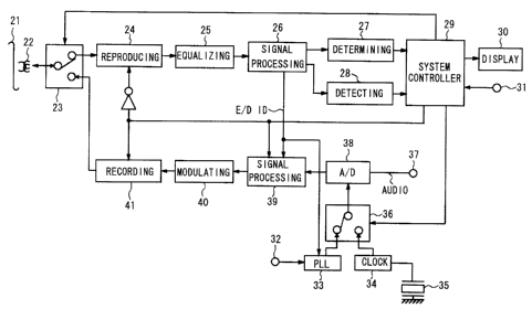
Fig. 8 shows the entire block construction of the
digital signal recording apparatus according to the
present invention. In the following description, it is
assumed that signals are recorded in record regions in
the same way as shown in Fig. 6. Data is recorded in
the predetermined record pattern shown in Fig. 6
(sampling frequency fs = 32 kHz and the number of
quantizing bits Qu = 12 bits). The record mode can be
determined by detecting an identification signal placed
in an ID region of data portion.
When an after-record mode command is supplied
from a terminal 31 to a system controller 5, as shown
in the flow chart for the signal process, the apparatus
enters the partial reproduction mode. Data recorded on
18
a magnetic tape 21 is reproduced through a magnetic head
22. At this point, since a magnetic head selecting
switch 23 is placed in reproduction position,
reproduced data (hereinafter referred to as
reproduction data) is amplified by a reproducing
amplifier 24. The reproduction data is supplied to a
reproduction equalizing portion 25. The reproduction
equalizing portion 25 equalizes the reproduction data.
The equalized data is supplied to a reproduction signal
processing portion 26. The reproduction signal
processing portion 26 performs signal processes such as
synchronous signal detection and error correction.
Thereafter, the sampling frequency fs, the number of
quantizing bits Qu, and so forth are detected.
The detected sampling frequency fs and the
number of quantizing bits Qu are supplied from the
reproduction signal processing portion 26 to an after-
record mode determining portion 27. The determined
result is supplied to the system controller 29. When
the sampling frequency fs and the number of quantizing
bits Qu are predetermined values (sampling frequency fs
- 32 kHz and number of quantizing bits Qu = 12 bits),
the after-recording can be performed. The reproduction
signal processing portion 26 detects an E/D ID. The
detected E/D ID is input from the reproduction signal
processing portion 26 to a fs clock generating PLL
portion 33 so as to control a frequency divider. At
19
3
this point, an audio PCM signal (Audio) that is
supplied to an A/D converting portion 38 through a
terminal 37 is controlled so that the same number of
samples as data portion in which the after-recording is
not performed are recorded. A synchronous signal is
supplied from the reproduction signal processing
portion 26 to a track number detecting portion 28. The
track number detecting portion 28 determines whether or
not to detect tracks TR6 to 10. The result is supplied
to the system controller 29.
The E/D ID generated in the reproduction
signal processing portion 26 is sent to a record signal
processing portion 39. The E/D ID is recorded along
with data. When the sampling frequency fs and the
number of quantizing bits Qu cannot be detected in
after-record enable state, the E/D ID generated in an
E/D ID generating portion 53 of the record signal
processing portion 39 is recorded along with data. At
this point, a switch 36 is switched so that the fs
clock oscillated by a crystal oscillator 35 rather than
the fs clock generation PLL portion 33 is used and
thereby the operation of the A/D converting portion 38
is performed.
When the after-record mode command is input
from the terminal 31 to the system controller 5, if the
after-recording cannot be performed, a warning alarm
displaying portion (warning) portion 30 that represents
2~~8~~~
that the after-recording cannot be performed displays a
warning and the after-recording is temporarily stopped.
When the record signal processing portion 39 detects
the tracks TR6 to 10 in the after-record region, the
magnetic head selecting switch 23 is placed to the
record mode position. Thus, the output signal of the
record signal processing portion 39 is supplied to a
modulating portion 40. The modulating portion 40
modulates the input signal corresponding to high
density magnetic recording and sends the modulated
signal to a recording amplifier 41. The amplified
signal is recorded on the magnetic tape 21.
When data has been recorded on tracks TR6 to
(namely, data has been recorded in an after-record
region), the system controller 29 sends a record end
signal to the reproducing amplifier 24, the record
signal processing portion 39, and the recording
amplifier 41. The record end signal causes the read
address generating portion of the record signal process
portion 39 to stop generating a read address. In
addition, the signal causes the record current to stop
flowing. Thereafter, the apparatus returns to the
partial reproduction mode and determines whether or not
to perform the after-recording. The above-described
process is repeatedly performed.
(9) Example of block construction of recording
portion
21
Fig. 9 is a block diagram showing an example
of the internal construction of the record signal
processing portion 39. As shown in the block diagram
showing the basic construction, banks of a memory 59
are controlled by a memory bank controlling portion 58.
A data bus DB and an address bus AB are connected to
various signal processing portions. The data bus DB is
connected to a block (not shown) through a terminal 60.
Likewise, the address bus AB is connected to a block
(not shown) through a terminal 61.
A sound (audio) signal is supplied from a
terminal 37 to an A/D converting portion 38. The A/D
converting portion 38 converts an analog signal into a
digital signal. Either the clock supplied from the
crystal oscillator 35 through the fs clock generating
portion 34 or the clock generated by the fs clock
generating PLL portion 26 corresponding to the detected
E/D ID is used for the operating clock of the A/D
converting portion 38. These clocks are switched by
the selecting switch 36 corresponding to a control
command issued from the system controller 29. In other
words, two types of clocks are switched corresponding
to a control command supplied from the system
controller 29.
When the clock of the fs clock generating PLL
portion 33 is selected in the after-record enable
state, the same E/D ID as the E/D ID of the data
22
2~~~~~~
portion that has been recorded is recorded along with
data. In the partial reproduction mode, the E/D ID
that has been detected by the reproduction signal
processing portion 26 is selected. The selected E/D ID
is supplied to the data bus DB through an ID write
buffer. At this point, the selecting switch 54 is
switched corresponding to a control command received
from the system controller 29 through a terminal 55.
When the selecting switch 36 has selected the clock of
the fs clock generating portion 34, a selecting switch
54 is controlled so that the E/D ID generated by the
E/D ID generating portion 54 is recorded.
The E/D ID that has been selected by the
selecting switch 54 is also supplied to an interleave
address generating portion 57. The interleave address
generating portion 57 controls an interleave address
counter so as to determine the number of samples at one
interleave region. The interleave address generating
portion 57 generates a data write address and supplies
it to the address bus AB through a write buffer.
Data that is output from the A/D converting
portion 38 is converted into a byte type data sequence
corresponding to the write address generated by the
interleave address generating portion 57 so that the
interleave signal processing portion 56 easily performs
the interleave process. The resultant data is supplied
to the data bus DB through a write buffer and written
23
~~48~83
to the memory 59 that is controlled by the memory bank
generating portion 58. Time shared data is supplied to
a parity generating portion 62 through a buffer. The
parity generating portion 62 generates a parity. The
generated parity is supplied to the data bus through a
parity write buffer and written to a predetermined
region of the memory 59.
A read address generated by a read address
generating portion 63 is supplied to the address bus AB
through a read address buffer. Data written to the
memory 59 is compressed on time axis and then read.
The resultant data is input to the modulating portion
40 through a read data buffer. The modulating portion
40 modulates the input data suitable for high density
magnetic recording.
The modulated data that is output from the
modulating portion 40 is supplied to a recording
amplifier 41. The amplifier 41 amplifies the input
data. The amplified data is recorded at a
predetermined record region on the magnetic tape shown
in Fig. 6. When a partial reproduction mode command is
received from the system controller, the operations of
the read address generating portion 63 and the
recording amplifying portion 41 are temporarily
stopped. At this point, the recording/reproducing
magnetic head selecting switch 23 is placed in the
reproduction mode position. Thus, the apparatus enters
24
2~~8~~3
the partial reproduction mode.
(10) Example of block construction of sampling
clock controlling portion
Fig. 10 is a block diagram showing an example
of the construction of a sampling clock controlling
portion. As described above, an ID signal is composed
of two bits. In this embodiment, the construction
thereof will be described with two parts. As a first
part, the construction for determining either the
number of E data (the number of E1 data and the number
of E2 data) or the number of D data (the number of D1
data and the number of D2 data) will be described. As
a second part, the construction for determining whether
the number of samples (the number of D2 data (1582) and
the number of E2 data (1622)) is farther from the
standard number of samples (1602) or the number of
samples (the number of D1 data (1592) and the number of
El data (1612)) is closer to the standard number of
samples (1602) will be described.
A frame reference signal FLID is supplied to a
phase comparing portion 72 through an input terminal
71. The phase comparing portion 72 compares the phase
of the frame reference signal FLID with the phase of
one of output signals of frequency dividers 76 to 79.
The resultant signal is supplied to a low-pass filter
73 so as to control a VCO 74 on the next stage. An
output signal of the VCO 74 is supplied to the A/D
~~~~~~3
converting portion and so forth as the fs clock. In
addition, the output signal of the VCO 74 is supplied
to the frequency dividers 76 to 79. The fs clock
supplied from the VCO 74 is output to the number-of-D1-
data frequency divider 76 (1592), the number-of-D2-data
frequency divider 77 (1582), the number-of-El-data
frequency divider 78 (1612), and the number-of-E2-data
frequency divider 79 (1622).
The outputs of the number-of-D1-data frequency
divider 76 and the number-of-D2-data frequency divider
77 are supplied to a selecting switch 80. The outputs
of the selecting switch 80 are switched corresponding
to the E/D ID supplied from a terminal 83. The E/D ID
is composed of two bits. Likewise, the outputs of the
number-of-E1-data frequency divider 78 and the number-
of-E2-data frequency divider 79 are supplied to a
selecting switch 81. The output of the selecting
switch 81 is switched corresponding to~the E/D ID
supplied from a terminal 83. The selecting switches 80
and 51 operate in association with so that either
smaller number of data (the number of D1 data and the
number of E1 data) than the standard number of samples
or larger number of data (the number of D2 data and the
number of E2 data) than the standard number of samples
is selected.
The outputs of the selecting switches 80 and
51 are supplied to a selecting switch 82. The output
26
~~~8~~3
of the selecting switch 82 is switched corresponding to
the E/D ID supplied from a terminal 83. In other words,
depending on the E/D ID supplied, either the number of
E data or the number of D data is selected. The output
of the selecting switch 82 is supplied to the phase
comparing portion 72. The selecting switches 80, 81,
and 82 for the frequency dividers use the E/D ID
detected in the reproduction signal processing portion
26 shown in Fig. 8.
Having described a specific preferred
embodiment of the present invention.with reference to
the accompanying drawings, it is to be understood that
the invention is not limited to that precise
embodiment, and that various changes and modifications
may be effected therein by one skilled in the art
without departing from the scope of the spirit of the
invention as defined in the appended claims.
27