Note: Descriptions are shown in the official language in which they were submitted.
WO 94/14304 ~ PCT/CA93/00481 ;v
214~'~0~
_1_
Industrial Material Processing, Electron Linear Aec~lgrator
The present invention relates to linear accelerators in general and, more
specifically, to electron linear accelerators for use in industrial material
processing.
BE1CKGROUNI) OF THE lJhfVENTION
The underlying science for the chemical and biological changes resulting from
exposure to electron and photon beams is well understood. A significant world
business which treats several billions of dollars of product annually, has
been created
by the exploitation of radiation technology. In general, electron accelerators
are used
to process biologically inert materials to improve the physical
characteristics of
materials while intense radiation sources emitting higher penetration photons
are used
to sterilize materials used in medicine. This differentiation of application
is directly
attributable to the Lower penetration of electrons and the high dose required
by most
chemical processes.
Accelerators in current use for processing materials operate in a direct
current
mode. They consist of two main classifications designated "electron curtain"
machines where the energy is restricted to less than 500 keV and "high
voltage"
machines where the maximum energy is S MeV.
Recently, industrial linear accelerators have been developed which are able to
accelerate electrons to 10 MeV with power levels up to 20 kW. They offer the
prospect of allowing electron accelerators to enter the lucrative medical
sterilization
market. A feature of the higher energy is the ability to convert the electron
energy
to photons with an efficiency which is more than twice that possible with 5
MeV
electrons. This property of the electron nuclear interactions is further
enhanced by
kinematic considerations which demand that the photon beam be projected more
in
L'te forward direction. This means that for a given beam power the photon flux
:.
on-axis is seven times more intense at 10 MeV than at S MeV.
All do accelerators stand off the high voltage across an insulated
accelerating
tube which contains the accelerating electrodes. Electrons entering the tube
are
accelerated to the final energy determined by the terminal voltage. The
weakness of
this system is that under intense radiation, electric charges will be created
on the
SUBSTITUTE SHEET
f
WO 94/14304 PCT/CA93/00481 :'r
::.:
2148'~~a
_2_ i
insulating tube and breakdown can occur. This breakdown will also occur under
the
electrical stress of the field itself. This is a direct consequence of the
fundamental
principle that the final electron energy, as defined in electron volts, is set
by".the
actual voltage which the insulator must withstand. In practice, for industrial
~ .
a
S accelerators the energy limit imposed by this limitation is S MeV. In
pushing these
limits, manufacturers are tempted to compromise reliability.
The linear accelerator (linac) does not suffer from this limitation. It
consists
of a copper tube with a series of specifically shaped discs or cavities along
its length.
The oscillating electric field is contained within this copper tube, which is
held at
ground potential. Depending on the frequency of oscillation and the gradient,
the
actual potential difference between any two points in the system does not
exceed
500 keV. An insulator is not required to sustain the high electric fields
associated
with this voltage. Existing industrial linacs work under a high level of
stress which
is undesirable to an industrial machine. This is a direct consequence of their
~ 15 historical pedigree rooted in particle physics research where emphasis is
on high
energy, high peak power, high field gradient and high klystron voltage with
lesser
consideration to high average power. The present invention addresses all of
these
limitations.
The present invention provides a new type of industrial linear accelerator
that
is conservatively inside the performance limits of accelerator technology.
Energy
gradients of research and medical linacs are typically 10 MeV/m. The gradient
of
the present invention is 3 MeV/m. Average power gradients have been tested in
operational electron linacs of 100 kW/m. The present invention provide
gradients of
15 kW/m. Beam currents during the pulse are of the order of lA in existing
pulsed
linacs while the present invention produces a beam current of about 100mA
during
the pulse.
These conservative ratings are made possible by using an L-band single ._ .
accelerator structure with a Wehnelt controlled electron gun, a graded-,B
capture ,
section directly coupled to a ~ =1 section and by driving the assembly with a
low-peak power, modulated-anode klystron operatod in a long pulsed mode. The
long
pulse has several advantages including the requirement for very modest peak
power
(2.5 MW), consequent low voltages on the klystron ( < 100 kV) and a modulated
WO 94/14304 ~ ;~ PCTlCA93/00481
-3-
anode which provides the pulse structure without having to transfer the power
as in
a conventional line modulator. The modest beam current means that beam-cavity
interactions, which commonly consume power by exciting beam break up .(bbu)
modes, are rendered impotent. These basic physics principles have been
embodied
S into an engineered prototype which has operated at 10 MeV and SO kW with an
availability of aver 97% for over 1500 hours of full power operation.
A very important aspect of the long pulse concept is the ability to use the
length of pulse as a variable and hence vary the average power of the beam
without
changing the physics of the process. The field gradient, the peak power and
the
current all remain the same. To vary the power of the machine at a constant
energy,
only the pulse length need be adjusted.
'' The novel feature associated with the long pulse is the ability to control
the
energy of the accelerated electrons during the pulse. The energy gained by the
,:..s
_<~~
PlPrtrnnc travPreino thr~ ctmrtmrE~ ie the line intPVr~l of t~P Plnrtr,n
F,a.l~i Thu
a,~
f 1 15 amplitude of the electric field is controlled using a magnetic field
probe to extract
some of the power of the cavity, using a crystal detector to measure the
amplitude
and, after comparing with a voltage setpoint, sending a signal to the rf drive
of the
klystron to adjust the klystron output. The setpoint thus becomes the
accelerator
~lr~
~;,k
x~::.~ enerev setvoint that can be directly linked to an international
standard. A maior
advantage of this method of energy control is the elimination of the need of a
~' magnetic bend to determine the energy and to assure that the possibility of
unwanted
excursions is eliminated.
Existing industrial rf linear accelerators operate with short pulses whereby
rf .
energy is transmitted to the accelerator in an open loop mode. In this mode,
changes
in beam current result in a change in the rf field level in the accelerator
and hence
in a change in energy. This is particularly true of accelerators that dominate
the
existing industrial rf linac market: In these accelerators, the power and
energy are
closely tied together and, as the power is increased, the energy must drop.
This is
a problem for many applications where a variation in the flow of product and,
hence,
the beam power is necessary but where the energy must remain fixed within
fight
limits.
'~F~'
WO 94/1404 PCT/CA93IU0481
2148r! ~ tf
Tight energy tolerances can be achieved with expensive power supplies
requiring very high stability. These systems use a time average of many pulses
to
determine a setpoint on the power supply for the energy. They are susceptible
to
changes in the pulse repetition rate. It is not possible to change the energy
during the
period of a single pulse with existing technology in the industrial linac
field.
Alternatively, the beam may be deflected by a calibrated amount in a magnetic
field.
This provides good energy selection following acceleration of the beam.
However,
existing systems do not allow the energy to be tightly controlled against the
voltage
droop that inevitably occurs during a pulse nor do they allow an independent
control
of the energy and power of the accelerator.
The present invention overcomes these difficulties by operating the
accelerator
~si in a long pulse mode with a fast, active feedback loop that can control
the rf field
during the accelerator pulse. The long pulse length, a pulse greater than 50
acs, can
be achieved with a modulated anode klystron. This provides sufficient time to
permit
regulation of the drive power to the klysuon and hence control the beam energy
at
i
the energy setpoint. The beam current, and hence the beam power, is controlled
by
a separate control loop independently of the energy.
The wide range of applications to which electron accelerators have been
subjected has led to unique machines designed for specific applications. Each
accelerator has its own set of replacement components. The purchase cost of an
accelerator and its replacement parts is high because of the non-recurring
engineering
cost associated with each part and the cost of inventory parts held by a
supplier is
high.
By way of background, a linear accelerator structure is composed of a series
of cavities in which microwave power is used to establish electromagnetic
fields. The
cavities are designed to concentrate the electric fields in a beam aperture
region of
the cavities to accelerate charged particles. The accelerating energy gradient
in the
cavities is typically 10 MeV/m. The device has poor reliability for industrial
use ,
beyond an energy gradient of IO MeV/m because electrical breakdown in the
cavities ,
disrupts beam acceleration.
The parameters that determine the output beam energy are length of the
accelerator structure and the electric field gradient. Beams of high-energy
are
WO 94/14304 < PCTICA93J00481
..
l
:a
"' obtained with several accelerator structures in series. The drawback of
having several '
1
accelerator structures in series is the need for additional control systems.
The phase
j
of the microwave fields in each accelerator structure must be controlled to
ensure,lhat
particles are maintained in synchronism with the accelerating fields
throughout the
':~; S accelerator. The microwave transmission characteristics of each
accelerator structure
depend on the dimensions and temperature of the device. These must also be
controlled precisely during fabrication and operation to obtain the desired
output beam
energy. The relative microwave power level in the different accelerator
structures
must be controlled. The control system is further complicated because of~ the
coupling between the control parameters of the machine: phase, microwave
transmission, accelerating field amplitude and accelerated beam current. These
contribute to the uniqueness of each linear accelerator and, consequently, to
the high
purchase cost of an accelerator and its replacement parts.
The present invention seeks to simplify the high-energy linear accelerator by
adopting a modular approach to address several applications with the same
basic
components. This allows the use of a single accelerator structure to achieve
beams
of high energy and eliminates the need for controlling the phase and microwave
transmission characteristics of a mufti-structure linear accelerator.
In accordance with this aspect of the present invention, the accelerator
structure is composed of three building sections: a beam capture section
module, a
coupler section module and an acceleration section module. The length and
number
of these modules, joined together to form a monolith accelerator structure,
are chosen
to meet the desired beam energy and power for a particular application. A
family of
high-energy accelerators which can address different applications, using the
same
building components, can then be made available.
The capture section is designed to accelerate and form beam bunches
synchronized with the microwave accelerating fields. The coupler section is a
device
usod to transmit the microwave power into the accelerator structure. The
acceleration
section is composed of a series of identical cavities in which microwave power
is
used to accelerate the beam. Accelerator sections are joined together with
flanges
designed to establish good electrical contact for the flow of microwave
current and
to provide an ultra-high vacuum seal. This is achieved by compressing a copper
~,;;:~'~:
WO 94114304 PCTICA93/00481 ''~'~'
. ~;=;:
. ..., .
,; ..
gasket between two pairs of stainless steel knife edges. The inner pair of
knife edges
are used for the electrical contact and the outer pair of laiife edges are
used for the
.s ultra-high vacuum seal. ,.
',The cross-sectional area of the electron beam leaving a high power
irradiator
<~~ S must be large to ensure good spot overlap during scanning. This is
accomplished
with the L-band accelerating system. Also, a uniform dose distribution is
required
at the product to be irradiated:
The dose distnbution is governed by software generated waveforms loaded
into an arbitrary function generator. Output from the signal generator
controls a
bipolar power supply which drives the scanning electromagnet.
The electric field strength within a long-pulse linac must be regulated to
within
a few percent despite changes in beam loading and significant changes in the
rf
system gain. This regulation must be maintained on a microsecond time scale
during
the pulsed application of rf power. Regulation is also maintained from pulse
to pulse.
' Good regulation is required to achieve predictable and reproducible
irradiator
performance: It is also beneficial in that overall electrical efficiency is
improved, by
maintaining a preset beam energy and avoiding beam spill that results from
energy-optics mismatch.
Heretofore; electric field regulation was achieved by using short pulses and
time-averaged control. Use of short pulses prevents the rapid drop of rf gain
from
having an appreciable effect within a pulse. Pulse-to-pulse regulation is not
done,
rather the field strength is averaged over many pulses and controlled to a
setpoint.
As indicated, this method does not provide any infra-pulse regulation. When
longer
pulses are present, adaptive waveform-shaping has been used in which the error
ZS observed during a pulse is used to correct the input drive signal for the
following
pulse. This method requires complex digital signal processing circuits.
The present invention proposes a controller which consists of broadband yet
simple proportional-integral analog control electronics and a single analog to
digital
converter (ADC) configured as a zero-droop sample and hold. An integration
term ..
is applied after a predetermined delay from the start of each pulse. After
another
short time-delay, the control signal is sampled and stored in the ADC. At the
end
of the pulse, the integration term is zeroed. At the start of the next pulse,
the control
21~8'~(?~
WO 94/14304 PCT/CA93100481 ':':~''.:.
7 - E. ,..
signal is set to the value stored in the ADC and the proportional control term
is r
engaged. The cycle repeats for each pulse. I'he method provides both fixed
I
infra-pulse regulation and pulse-to-pulse regulation with simple electronics.
Storing
M
the control signal for use on the subsequent pulse and the staged deployment
of the
S controller terms, effectively removes the dead-time between pulses, thus
attaining the
performance of a continuous system with a pulsed system.
The power for a pulsed electrical load is often derived from the electrical
energy stored in a capacitor bank. The high discharge pulse current generally
causes
the voltage on the capacitor to droop significantly during the pulse, thereby
changing
the operation of the driven load during this time. . A klysuon is an example
of such
a driven load and a klystron with a modulating anode is often driven by a
circuit
which includes a switch, a pull-down resistor and the capacitor bank to store
the
charge for the current pulse through the klystron. When the switch closes, the
klystron conducts current and can be used to amplify rf power. The declining
voltage
during the pulse affects both the cathode potential and the modulated anode
potential
in such a manner that the accelerating potential, i.e. the difference between
the two,
changes during the pulse. This circuit is not adequate if a controlled,
.predetermined
change in the accelerating potential is desired.
It has beewpmposed to employ a programmable variable-voltage power supply
20' to achieve a controlled accelerating potential. The power supply would be
commanded to change its output voltage in a predetermined manner during the
pulse.
This system has proven to be costly and susceptible to reliability problems
due to its
complexity and number of active components.
' The present invention proposes the provision of a switch tube triggered by a
low power switch in order to divert a part of the current that flows through
the 3
E
resistor during the pulse through a grid-leak resistor in the switch tube
circuit and
from there through a diode to a small capacitor connected to ground. With the
current during the pulse flowing through the capacitor, the magnitude of the
voltage
on the capacitor will decrease, drawing the modulated anode voltage with it.
By the
proper choice of grid-leak resistor, capacitor and the output impedance of the
bias
supply, the rate of voltage decrease during the pulse can be set to a
predetermined
.. .
WO 94/14304 PCTlCA93100481
':
214~'~Qy ::
;:l9 6
value. Although this implementation involves the use of a switch tube, it will
be
4
S
understood that the same principle can be used with transistors as switching
elements.
'
Control of the temperature of an accelerator gun cathode is required in order
to maintain the cathode electron emission at a sufficiently high value and to
prevent
i
S over-heating from damaging the cathode or shortening its life. Accelerator
electron
gun cathodes are operated at elevated temperatures ( > 1000°C) with
heating provided
by electrical current in a filament heater circuit. Depending upon the cathode
type,
the electron emission for a given electric potential distribution increases
with
increasing temperature. This emission characteristic is non-linear,
approaching
saturation at and above the operating temperature. Operation at excessive
_- temperatures shortens the life of the cathode and increases the risk of gun
arcing due
to deposition of cathode material on insulating surfaces.
i
n'I,
v Radio-frequency linear accelerators accept injected electrons for forward
acceleration and reject a fraction of the injected electrons. For accelerators
not
having a beam "buncher", the rejected electrons may be returned to the gun
with
significantly greater energy than they had on injection. This backwards-
accelerated
t ' beam represents a small power loss to the accelerator and a significant
power source
to the electron gun. For an axi-symmetric geometry, a fraction of the
backwards
accelerated electrons will impact on the gun cathode, deposit their energy and
increase its temperature. Depending on the injection voltage and injection
optics, this
rejected beam may become a significant fraction of the power supplied to the
cathode
,
heater, altering the operating conditions.
In addition to the backwards accelerated electron beam, the accelerator will
'~ also accelerate ions generated from the background gas present in the
accelerator.
While the accelerator is not optimized for ion acceleration, some ion
bombardment
~a ~ will occur. The gas present in the electron gun is ionized by the
injected electron
beam and the backwards accelerated beam produces a "column" of ions in front
of
the cathode. These ions will be accelerated by the cathode potential to impact
the ,
.'cathode and other surfaces at negative potential.
;,
-,3 30 For most applications developed to date, the average backwards
accelerated .
y
beam power is a small faction of the cathode heater power due to the low duty
cycle
(low average beam power) of the accelerator. Where mitigating measures are
:,;>.;
WO 94/14304 1 ~ $ ~ ~ t j PCT/CA93/00481
:.::..:.~ L.,:;.,..:.:.
_ 9 _ i:.:....,
..
required (electron tubes), hollow cathode constructions have been employed or
proposed to reduce the portion of the reverse beam impinging on the cathode.
In 1
addition, occluding optics may be employed to reduce the portion of the
backwards i
accelerated beam that impacts the cathode. Moreover, it is possible to reduce
the
energy of the electrons returning to the cathode by operating the cathode at a
greater v
injection voltage, requiring the electrons to "climb the coulomb barrier"
before
reaching the cathode.
As the average power of the accelerator is increased, the fraction of the
cathode heater power that the power deposited by the backward accelerated
beams
l0 represents grows to become significant. Adjustment of the injection optics
by either
mechanical or electromagnetic means reduces the back-heating fraction, but
does not
eliminate the phenomenon. At some finite average power, the back-heating
effects
prove limiting to further increases in average beam power without deleterious
consequences.
The present invention estimates circuit resistance based on measurements of
the gun cathode filament circuit voltage and current. A control loop is used
to
maintain the resistance at a setpoint value by adjusting the filament power
supply
current setpoint. This control loop may be implemented either in hardware or
as a
software control program of the accelerator, The filament circuit resistance
serves
to stabilize the cathode temperature and hence the electron gun performance
under the
influence of backward accelerated beam and/or ion bombardment. This resistance
is
used as an imperfect monitor of the cathode temperature.
Fast shutdown systems are required for linear accelerators to protect high
power subsystems from damage. In particular, the shutdown systems are required
to
discharge the electrical energy stored in the rf power system in the event of
anomalous conditions, to extinguish arcs in the rf power delivery system,
preventing
damage to the waveguide and components, to extinguish arcs in the linear
accelerator,
minimizing damage to the interior of the accelerator and protecting the rf
power
system from reflected power, to prevent anomalous rf drive conditions from
damaging
expensive components, to prevent deposition of excessive accelerated beam
current
on sensitive elements of the accelerator beam delivery system, and to disable
accelerated beam current in the event of a failure of the beam dispersal
subsystem.
WO 94/14304 PCTlCA93/00481
->.:~::
21487
- io -
The topology of a modern high-power accelerator has the major components
distributed as appropriate to the requirements of the facility. In such a
facility, the
components that contribute to the decision that a fault condition exists may.,
be
separated from each other as well as from the logical point of action for the
decision. ~ .
I
The speed of decision and maximum delay toy the protective action required are
different depending on the characteristics of the fault condition and the
tolerance of
the affected components for the resulting stress. In many cases, the speed of
detection and action exceeds the capabilities of the process control system by
several
orders of magnitude: a few microseconds as opposed to tens or hundreds of
milliseconds. Hence, fast hard-wired protection systems are required.
Conventional protection practice . depends; in part, on the design of the
accelerator and the limitations imposed by the component manufacturer. For
example, until recently, most control systems have been arranged with each
signal
carried by individual wires to the control room for monitoring and alarm
functions.
l5 Modern distributed control system designs permit reducing the number of
signal
cables that enter the control room, with most data being acquired remotely and
telemetered via multiplexed digital communication from clustered points. An
alternative practice is to provide a high speed detection function at the
point of
measurement, relay the decision to the control room where it may be logically
conditioned and relay the instructions to the protective action point.
The multiple cables required for the conventional schemes carry cost penalties
for the cable and installation, have multiple length signalling delays, and
are
F
vulnerable to the electromagnetic interference unless high cost optical-fibre
systems
are used. For specific types of faults, the associated electrical disturbance
may be
sufficient to defeat the communication function and to prevent protection. The
system
may also be vulnerable to spurious trips arising from external sources of
electromagnetic interference.
..-: :.
t . ..
These difficulties are overcome by the present invention by the provision of .
a single communication cable configured as a fail-safe current loop and used
for high
3Q speed signalling of many protection decisions to one or more activation
devices. The ,
optically-isolated communication in the fail-safe sense is achieved with high
speed by
using a complementary logic drive to discharge the base capacitance of the
primary
.., ., WO 94/14304 PCT/CA93/00481
,:..:.
-11-
optical isolator with a second optical isolator. The noise immunity for each
decision
is selected on the basis of the impact of the related fault condition
permitting a unique
false-alarm/missed-alarm tradeoff for each condition.
The high speed protection system of the present invention employs several key
elements: It includes a current loop that is optically-isolated at each
connection and
chained through each decision device and action module. 'lfie current loop is
enabled
by the supervisory control system to permit testing and logical control. The
current
loop is arranged to be fail-safe in that a loss of continuity in the loop
cable causes the
action device to operate and the head-end control to latch the loop in an open
state ,
until it is reset. Decision modules employ the full sensor bandwidth available
for
detection and :provide a selectable sustain criterion for the decision as well
as limited
provision for logical conditioning based on parameters monitored in other
modules.
A high quality digital communication cable is used for the current loop with
the shield
connections arranged for high noise immunity. Fault detection circuits are
conditioned on the current loop being closed to ensure that, within the
signalling
delay; only he first fault to be detected is latched for diagnostic purposes.
Each
signal used for a protection function is separately measured by the
supervisory
process controller to validate the signal.
WO 94/14304 PCTICA93/004$1 ~:-;y:~.~
-: ':
_ I2_
SUMMARY OF THE INVENTION
Thus, one aspect of the present invention provides a linear accelerator for
use
in industrial material processing, comprises an elongated resonant electron
accelerator
structure defining a linear electron flow path and having an electron
injection end and
t
an electron exit end, an electron gun at the injection end for producing and
delivering
one or more streams of electrons to the electron injection end of the
structure during
pulses of predetermined length and of predetermined repetition rate, the
structure
being comprised of a plurality of axially coupled microwave cavities operating
in the
~c/2 mode and including a graded-~ capture section at the injection end of the
structure for receiving and accelerating electrons in the one or more streams
of
electrons, a ~= I section exit section at the end of the structure remote from
the
capture section for discharging accelerated streams of electrons from the
structure and
an rf coupling section intermediate the capture section and the exit section
for
coupling rf energy into the structure, an rf system including an rf source for
converting electrical power to rf power and a transmission conduit for
delivering rf
power to the coupling section of the structure, a scan magnet disposed at the
exit end
of the structure for receiving the electron beam and scanning the beam over a
predetermined product area and controller for controlling the scanning magnet
and
synchronously energizing the electron gun and the rf source during the pulses.
20' Another aspect of the present invention relates to an electron gun for use
in
an electron accelerator in producing an electron beam, the electron gun
comprising
an anode plate having a central aperture, a dispenser cathode for emitting
electrons
and a Wehnelt focusing-electrode assembly for focusing electrons emitted by
the
cathode through the aperture of the anode plate, a resistive heater associated
with the
25' cathode for heating the cathode, means responsive to a control signal for
energizing j
the heater, and control means for generating the control signal pulses at a v
predetermined repetition rate and for predetermined durations to cause the
electron
c. .
gun to emit electrons during the duradons, the control means being responsive
to a
i
signal representative of the resistance of the heater to cause the heater
energizing r
30 means to energize the heater to deliver with only sufficient energy to
maintain the
resistance of the heater at a predetermined value.
- . WO 94114304 ~ i~ PCT/CA93/00481 y
... .'°.: ., .
. :.. : ,:
_ 13 _ ~:~ -
F
A further aspect of the present invention relates to a device for measuring
the
electrical current of the electron beam exiting from a linear accelerator, the
device
j.
comprising a beam line section for transporting an electron beam and for
connection
M
to but electrically insulated from an additional portion of the beam line, an
axial gap
;.
in the beam line section, a tubular member extending across the gap, a beam
current
toroid concentricahy disposed about the beam Iine section; an electrical
inductor
extending axially between the toroid and the beam line section and having
opposed
ends for producing an electrical signal representative of the current of an
electron
beam in the beam line section, and a control system connected to the opposed
ends
of the conductor and responsive to the magnitude of the signal to adjust a
means for
producing the electron beam so as to maintain the beam current at a
predetermined
value.
A still further aspect of the present invention relates to feedback control
system for maintaining the beam line current from an accelerator structure
within
predetermined limits, the feedback control system including a pulse generator
for
generating reference current pulses synchronized and coincident with beam
current
pulses to be measured and an electrical conductor extending axially between a
beam
current toroid and the beam line for carrying the references pulses, the
reference
pulses being of the opposite polarity to that of the beam line current so that
the
current in a beam line current measuring conductor is the differential between
the
beam line current and the current of the reference pulses, the control system
being
operable to output a control signal to the pulse generator tending to reduce
the
differential to zero.
r,,r. ,.,;,. ,. , .,., ..-,;........., ..,:. ,;., ,:. ..... . , ;..,...
......._.. .,...... . ._.,__,. "~..,..,".".....
_.,::.
r""::.,
WO 94!14304 PCTICA93/00481
i. w: .
~g~7 ~
- 14-
i
BRIEF DESCRIPTION OF THE DRAW~1GS
i
The foregoing and ocher features of the invention will become more apparent
from the following description in which reference is made to the appended
drawings,
wherein: '
FIGURE 1 is a block diagram diagrammatically' illustrating the basic systems
according to the preferred embodiment of the present invention;
FIGURE 2 is a block diagrammatic illustration of the basic components of the
control system according to the preferred embodiment of the present
invention;
FIGURE 3 is a front elevational views of a linear accelerator according to the
preferred embodiment of the present invention;
FIGURE 4 is a side view of the linear accelerator illustrated in FIGURE 3;
FIGURE 5 is a longitudinal cross sectional view through an electron gun;
FIGURE 6 is an enlarged cross sectional view of the cathode assembly of the
electron gun illustrated i~ FIGURE 5;
FIGURE ? is a cross sectional view of the rf coupling section of the
accelerator, rf
elbow and rf window assembly according to the preferred embodiment of the
present Invention;
FIGURE 8 is a top view of the coupling assembly of FIGURE 7;
FIGURE 9 is a cross sectional view taken along lines 9-9 of FIGURE 8;
FIGURE 10 is a perspective view of the industrial material processing linear
accelerator of the present invention illustrating the high power rf
transmission
system connected to a vertically oriented accelerator section disposed over a
product conveyor;
FIGURE 11 is an exploded, perspective view illustrating the high power
klystron,
modulator according to a preferred embodiment of the present invention;
FIGURE 12 is a circuit diagram of a klystron drive circuit according to the
preferred y-
embodiment of the present invention;
FIGURE 13 is a front elevational view diagrammatically illustrating the
electron gun ' ,
cabinet in accordance with the preferred embodiment of the present invention;
FIGURE 14 is a side elevational view of the electron gun cabinet illustrated
in
FIGURE 13;
' ..
WO 94/14304 PCT/CA93/00481
...,; .. ,..w..
-:'>
- 1S - I
FIGURES 15 and 16 are front and back elevational views, respectively,
diagrammatically illustrating an rf driver cabinet in accordance with the
preferred embodiment of the present invention; .~
FIGIJRFS 17 and 18 are front and side elevational views, respectively,
S diagrammatically illustrating rf cabinet in accordance with the preferred
embodiment of the present invention;
FIGURE 19, is an electrical schematic diagrammatically illustrating a control
circuit
for generating a pulse control signal according to the preferred embodiment
of the present invention;
FIGURES 20 and 21 are front and side elevational views, respectively,
diagrammatically illustrating the accelerator cabinet in accordance with the
preferred embodiment of the present invention;
FIGURES 22 and 23 are front and side elevational views, respectively,
diagrammatically illustrating the klystron cabinet in accordance with the
preferred embodiment of the present invention;
FIGURE 24 is a diagrammatic view of the operation panel in accordance with the
preferred embodiment of the present invention;
FIGURE 25 is a partially broken, cross sectional view of a portion of the beam
line
about which a beam current toroid is positioned according to the preferred
embodiment of the present invention;
FIGURE 26 is a cross sectional view of an electrically insulating gasket
disposed two
Conflat flanges in the beamIine according to the prefeiTed embodiment of the
present invention; and
FIGURE 27 is a schematic of a circuit for malting a differential measurement
used
to determine the accelerated beam current according to the preferred
embodiment of the present invention.
. i-:
r;::. . .
y
t.
:.a..S,,:c,.,.
WO 94/14304 PCT/CA93/00481
.,,
,,.
a..
21 ~ 8'~ 0 ~ ~,::,;
4... ~.
- 16-
DESCRIPTION OF PREFERRED EMBODIMENT
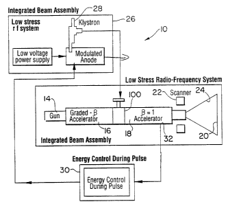
FIGURE 1 illustrates the basic operating components of the linear accelerator
of a preferred embodiment of the present invention: The accelerator includes
an '
L-band single accelerator structure 12 having, at one end, a Wehnelt
controlled
,:
i
5 electron gun 14 which injects electrons into a graded-S capture section 16
which is
directly coupled to a ~ =1 section 18. The accelerator accelerates the
electrons to
form a beam of predetermined energy. The beam passes out of the accelerator
structure and through a scan magnet 22 which sweeps it in a predetermined
manner.
The beam then passes out through a scan horn 24 through an exit window 20 onto
10 product carried by a conveyor 21. A low stress rf system 26 includes a
modulated-anode klysuon 28 operated in a long pulsed mode (a pulse greater
than
about 50~cs) generates the electromagnetic field within the accelerator
structure to
accelerate the electrons with low peak power as explained more fully later.
A novel feature associated with the long pulse is the ability to control the
energy of the accelerated electrons during the pulse. This feature provides
sufficient
time to permit regulation of the drive power to the klystron and hence control
the
beam energy at the energy setpoint. The beam current, and hence the beam
power,
is controlled by a separate control loop independently of the energy. The
energy
gained by the electrons traversing the accelerator structure is the line
integral of the
electric field. Thus, the amplitude of the electric field is controlled by an
energy
control system 30 using magnetic field probes 32 to extract some of the power
of the .
cavity, using a crystal detector to measure the amplitude and, after comparing
with
a voltage setpoint, sending a signal to the rf drive of the klystron to adjust
the
klystiron output. The setpoint thus becomes the accelerator energy setpoint
and can
be directly linked to an international standard. A major advantage of this
method of
energy control is the elimination of the need of a magnetic bend to determine
the
energy and to assure that the possibility of unwanted excursions is
eliminated.
The long pulse has several advantages including the requirement for very
modest peak power (2.5 IviV~, consequent low voltages on the klystron (less
than
100 kV) and a modulated anode which provides the pulse structure without
having to . i
transfer the power as in a conventional line modulator. The modest electron
beam
current means that beam-cavity interactions, which commonly consume power by
WO 94/14304 e~ PCT/CA93/00481 rs~'~"
.:;."-: ; r,'.
17 j.
exciting beam break up (bbu) modes, are rendered impotent. Another aspect of
the
long pulse concept is the ability to use the length of pulse as a variable and
vary the j
beam average power without changing the physics of the process. The field
gradient,
the peak power and the current all remain the same. To vary the average power
of
S the machine at a constant energy, only the pulse length need be adjusted. a
One aspect of the present invention seeks to simplify the construction of a
high-energy linear accelerator by adopting a modular approach to address
several
applications with the same basic components. This allows the use of a single
accelerator structure to achieve beams of high energy and eliminates the need
for
controlling the phase and microwave transmission characteristics of a mufti-
structure
linear accelerator. To that end, the accelerator structure is composed of
three
building sections: a beam capture section module, a coupler section module and
an
acceleration section module. The length and number of these modules, joined
together to form a monolith accelerator structure, are chosen to meet the
desired
beam energy and power for a particular application. A family of high-energy
accelerators which can address different applications, using the same building
components, can then be made available.
The capture section is designed to accelerate and form beam bunches
synchronized with the microwave accelerating fields. The coupler section is a
device
used to transmit the microwave power into the accelerator structure. The
acceleration
section is composed of a series of identical cavities in which microwave power
is
used to accelerate the beam. The accelerator sections are joined together with
flanges
designed to establish good electrical contact for the flov~i of microwave
current and
to provide an ultra-high vacuum seal. This is achieved by compressing a copper
gasket between two pairs of stainless steel knife edges. The inner pair of
knife edges
are used for the electrical contact and the outer pair of knife edges are used
for the
ultra-high vacuum seal.
i:.:.
The energy of the electrons delivered by the accelerator is achieved by v
accelerating electrons with radio frequency (rf) power in a resonant
accelerator
structure comprised of coupled microwave cavities which resonate in the ~/2
mode.
Two types of cavities are used in the structure: accelerating cavities and
coupling
cavities. The accelerating cavities are specially shaped to impart maximum
energy
WO 94/14304 PCT/CA93/00481 _ ~~'
214870
_ 18 _
to the electrons passing down the axis and to minimize the loss of rf power in
the
cavity walls. The coupling cavities are located between the accelerating
cavities and
couple the rf power between the accelerating cavities. To provide a SO kW
electron
beam at an energy of 10 MeV, the accelerator structure is provided with 29
accelerating cavities and 28 coupling cavities. The accelerating and coupling
cavities
are located on the same axis, i.e. the structure is on-axis coupled. As
illustrated in
FIGURE 1, rf power is introduced into the centre accelerating cavity, i.e.
midway
between the ends of the swcture, and propagates in both directions to the ends
of the
structure where it reflects to set up standing waves in a ~/2 resonant mode,
i.e. the
rf field in each cavity is ul2 radians (90°) out of phase with adjacent
cavities. This
results in almost a zero rf field in the coupling cavities and maximum rf
field in the
accelerating cavities. The electric field in the accelerating cavities is
concentrated
across nose cones (not shown) where it is used to accelerate the electron
beam.
In principle, the structure could be supplied with continuous wave (cw) rf
power to generate a continuous beam of electrons. However, an accelerator
structure
. operated continuously under the conditions mentioned below would generate 1
MW
of electron beam which is much greater than is presently required for
commercial
irradiation. To retain the efficiency and reduce the beam power, the
accelerator is
operated at a 5 % duty factor. Pulses of electron beam that are sustained for
200 ~s
. are generated at a rate of 250 Hz. The rf power source is pulsed at the same
rate to
maintain efficiency. The nominal parameters of the preferred embodiment of
linear
accelerator constructed according to the present invention are:
Electron Beam Power . 10 to 50 kW
Beam Energy . 10 MeV
Duty factor . 5 96
Pulse Length . 50 to 500 acs a
Pulse Repetition Frequency . 1 to 500 Hz .
Peak Beam Current . 100 mA
RF Frequency . . 1.3 GHz
Strscture Type . standing wave on-axis coupled
The rf power system that supplies rf power to the accelerator structure is the
largest support system required for operation of the accelerator. Its main
components
include the high power klystron, the modulator and the high voltage klystron
Power
Supply (KPS). These ace high power devices that must be carefully controlled
to
WO 94/14304 1 (~ g ~ O ~ PCTICA93/00481 '''~'v''v'
_19_
provide the required rf power to the accelerator structure and to avoid damage
to high
power components.
The accelerator is controlled by six systems, generally il.lustrated~ m
FIGURE 2, including a Programmable Logic Controller 40, a Human Machine
Interface 42, a Master Timing Generator 44, a High Speed Signal Processing
system
46, a High Speed Machine Protection system 48 and a Personnel Safety System
49.
The logic controller provides centralized control of the accelerator. It is
able '
to take actions on analog and discrete variables with response times greater
than 500
ms and I00 ms, respectively. Human machine interface 42 is a video display
computer connected to the logic controller to provide operator input and
readout.
Timing generator 44 under the control of the logic controller provides timing
pulses
which switch rf and high voltage devices and provides sampling pulses for
measurement of pulse parameters. Signal processing system 46 consists of
dedicated
electronic circuits to provide measurements of pulse parameters. Tlte inputs
to the
signal processing system are the sampling pulses from the timing generator and
the
pulses o be measured. The output is a voltage that is held constant between
pulses
and updated during each pulse. High speed machine protection system 48 also
consists of dedicated electronic circuits which switch off the rf power or
high voltage
on a microsecond time scale to prevent damage to the high-power electronic .
components. The personnel safety system 49 is comprised of relay logic and
provides
interlocks to protect personnel from hazards. It ensures that areas with
radiological,
rf radiation or high voltage hazards are secure before the accelerator is
started.
The accelerator consists of nine manufactured subsystems and a shielded x
facility to provide protection from the radiological hazards. A generic
shielded
facility is first described, next the accelerator, located inside the
shielding, and then
the support equipment, located outside the shielding and finally the operating
console.
~.~:::.::.
~.
F
i
W 41 04. PCTICA93100481 ~v=:=v
2 ~~~~0
20 _ t :.,.
Shielded Facility
As already mentioned, the preferred embodiment of the accelerator produces
a SO kW beam of electrons that have an energy of 10 MeV. This beam is lethal
and j
shielding must be provided to protect personnel. Bremsstrahlung X-ray
radiation is
produced by electron beam spill as it is accelerated through the acceleratar,
when it
passes through the beam window and when it impinges on the product, conveyor,
beam stop and other accelerator components. Activation of accelerator
components
and product is possible but with careful selection of component material and
restriction of the product to be irradiated, activation can be controlled to
low levels.
Most uses of the electron beam require the beam io pass from the accelerator's
vacuum envelope, through air, and onto the product. Interaction of the
electron beam
with air generates ozone (O,) and nitrous oxides which are hazardous.
To provide radiological protection, the accelerator is surrounded by a shield
made from normal density concrete. A conveyor 21 usually carries product
through
the beam but transport of bulk material via a pipe or in continuous form such
as cable
is also possible. The praduct to be irradiated is transported through a
concrete maze,
irradiated by the electron beam, and transported out. through a concrete maze.
Water
cooled beam stop 144, located below conveyor 21, absorbs the beam when product
is not present. Ventilation is arranged to provide an air flow from the maze
entrance
and exit, toward the irradiation area, and then out an exhaust duct. Fresh air
is
supplied at the maze entrance and exit and also to the area around the
accelerator.
Accelerator
The accelerator is illustrated in FIGURES 3 and 4. The electron gun 14, x
electron gun optics assembly 58, accelerator injection section 84, accelerator
coupling
section 100, waveguide elbow 108, accelerator exit section I10, microwave
window
assembly 114, and ion pumps 126 form a vacuum envelope having a base pressure
of 10'8 Torr (about 1 ~cPa). The remaining components are mechanical supports
and
the electron-beam delivery system.
With reference to FIGURF.,S 5 and 6, electron gun 14 is mounted in a welded
stainless steel housing 50 having Conflat flanges 52 for mounting the gun, and
port
54 for connection to a gun ion pump, a port 56 for connection to a getter
vacuum
WO 94!14304 PCT/CA93/00481
..., f..::::.:..:
- 21 - y.
pump and for joining the housing to an electron-gun optics assembly 58. An
anode
plate 60 with a central. aperture 62 is mounted just behind a mounting flange
64.
Mounting Flange 64 is formed mth channels (not shown) through wtuch coq,~.~ng
;
water flows to control the anode plate temperature. The electron gun includes
a
dispenser cathode 66 and Wehnelt focusing-electrode assembly 68. Thus,
electrons
emitted by the cathode 66 are focused into aperture 62 in the anode plate and
are
injected into the first accelerator cavity. A nominal voltage of -40 kV do is
applied
to the cathode. Between accelerator pulses, electron emission from the cathode
is
cut-off by holding the voltage on the Wehnelt electrode at about -3 kV with
respect
to the cathode. Controlled electron emission during the accelerator pulse
occurs with
the voltage on the Wehnelt electrode at about -100 V with respect to the
cathode.
Adjustment of the Wehnelt voltage by the control system controls the current
that is
injected into the accelerator. An injection current of about 300 mA peak is
required
from the gun for full power operation.
In a high-power rf powered accelerator where electrons are injected into the
accelerator from an electron gun, which contains a dispenser. cathode assembly
as
described above, throughout the rf cycle, some of the electrons are stopped by
the
electric field in the first accelerator cavity during the negative portion of
the rf cycle
and are accelerated backwards towards the cathode with energies in excess of
those
at which they were injected. .Some of these electrons travel on a path near
enough
to the axis that they pass back through , the anode aperture and strike the
cathode
where they deposit their kinetic energy as heat. In accelerators of this type,
the
electrons are emitted from the hot cathode surface which is held at a constant
temperature of about 1,000°C. The temperature is obtained from and
maintained by
t
a resistive heater 70 which is embedded in the cathode assembly. The heater is
driven by a power supply 72 typically operating at a current of 2.SA and a
voltage
of 8V. In a low power accelerator, the effects of these electrons are not
generally
noticed. In a high powered accelerator, where the duty cycle of the
accelerator is
several percent, the energy deposited in the cathode by these electrons may be
sufficiently high to cause overheating of the cathode with subsequent damage,
shortened lifetime and large outgassing which can prevent operation of the
accelerator.
WO 94/14304 PCT/CA93/00481 ~~~i'
,~ <, ;:''
~~.~~~t~~ - 22 -
According to one aspect of the present invention, this problem is overcome by
decreasing the power transmitted to the cathode by the power supply to exactly
compensate for the power deposited by the back-streaming electrons from. the
accelerator. The total power into the cathode, i.e. from the resistive heater
and the ~ ~ -~
back-streaming electrons, then maintains the constant cathode surface
temperature
required for long lifetime and good operating characteristics. This is
achieved by
determining the temperature of the cathode. This method relies on the fact
that the
electrical resistance of the resistive heater, which is typically 3.5 ohms, is
a strong
function of the cathode temperature. Hence, if the resistance is maintained at
a fixed
value, the temperature of the cathode will also be held at a constant value.
Both the
voltage across the heater and the current are therefore measured accurately
during
operation and are fed to the programmed logic controller which uses the ratio
of these
two values to calculate the resistance of the heater. As the accelerator is
started up
from a cold start to some desired power, a control loop is set up to reduce
the current
from the pov~ier supply to the heater so as to maintain a constant resistance.
This then
ensures a constant temperature on the cathode surface.
Optics assembly 58 includes a welded stainless steel housing 80 with conflat
flanges 64 and 82 at its ends. Flange 64 is secured to the electron gun
housing and
flange 82 is socured to accelerator injection section 84. Two steering coils
86 and
a gap-lens focus-magnet 88 on the assembly steer and focus the electron beam
from
the eloctron gun. As already mentioned, cooling water flows through channels
in
front flange 64: The steering and focusing coils operate at low voltage from
power
supplies located in rf and accelerator cabinets, respectively, described
later.
3
With reference to FIGURE 3, an accelerator injxtion suction 84 includes 13
full and one half accelerating cavities. They are made from oxygen free high
conductivity (OFHC) copper segments that are brazed together. Stainless steel
flanges are also brazed at the two ends of the section. One half of each
cavity
segment is an accelerating cavity and the other half is a coupling cavity so
that, when
brazed together, the segments form alternating accxlerating and coupling
cavities.
Before brazing, each cavity is tuned to provide a structure in which all of
the cavities
resonate at the same frequency. The first four cavities vary in length to
accommodate
the change in electron velocity during acceleration and to maintain
synchronism
.. .,. . v ... °. v:,. ..., . .: . .. _._. __ _._
.. ,~a ::. _. .. :: .:. ~.: . : .: .: : . ; . ~ . . , : . . . . . ,
between the electrons and the rf electric field. The balance of the cavities
have the
same length because relativistic velocity has been achieved after the first
four cells
and further energy is achieved mainly by increasing the mass of the electrons.
Cooling channels (not shown) for carrying deionized water are formed as an
integral
S part of the copper segments. Connections from the cooling channels to
cooling
headers 138 are provided on the stainless steel flanges. Connections to the
vacuum
manifold are provided by three stainless steel vacuum ports (not shown) with
conflat
flanges. Two rf field probes 32 (see FIGURE 1) are provided for sampling the
rf .
field in the injection section.
With reference to FIGURES 3 and 7, accelerator coupling section 100
comprises two half accelerating cavities 102 and one full accelerating cavity
104 made
from OFHC copper with a stainless steel flange on either end. An iris and a
tapered
waveguide, described below, provide rf coupling to a waveguide elbow 108. The
coupling section also includes integral cooling channels, a vacuum port (not
shown)
and an rf field probe (not shown).
An accelerator exit section 110 comprises 13 full and one half accelerating
cavities. The construction of the exit section is identical to the injection
section
except that all cavities are of the same length. The exit section includes
three vacuum
ports (not shown) and three rf field probes (not shown) are provided.
A welded stainless steel scan horn 24 is connected to the accelerator exit
structure via a stainless steel bellows (not shown). The electron beam is
scanned in
the scan horn by the scan magnet 22. Flanges at the wide end of the horn hold
a
thin, 0.13mm (0.005 inch), titanium exit window 20 (FIGURE 1) that permits the
v
r
electron beam to pass from vacuum to atmosphere. Tubes (not shown) on the
outside
of the horn and channels in the flange carry water to provide cooling.
High power accelerators require rf power from an rf transmitter, klystron 28 ;
in this case, to be fed to the vacuum cavity in the accelerator so as to, in
turn, '
generate the electric fields that accelerate the electron beam. The power is
fed via
k
a rectangular waveguide 112 (see FIGURE 10). To prevent voltage breakdown in s
the waveguide, the waveguide is normally filled with a pressurized insulating
gas, v
such as sulphur hexafluoride. A microwave window assembly I14 is used to keep
this gas from entering the accelerator while permitting the transfer of rf
power. The
WO 94/14304 PCT/CA93100481 ~.'v'''
t ......
. . ;.: :::...:...
. , : .,
24 - ~.....
assembly consists of a metal flange 116 and an aluminum oxide ceramic disc
118,
normally circular, brazed to the flange. During high power operation, it has
been
found that scattered electrons and low-energy x-rays from the electron beam
allow
high electric fields to be generated within the ceramic material. These fields
become
sufficiently large that, after some time, the ceramic will electrically
discharge. The
discharge leads to damage within the window that destroys its ability to act
as a
barrier between the vacuum of the accelerator and the pressurized gas in the
waveguide:
To overcome this problem, the window assembly is placed at a location where
electrons and x-rays cannot travel by line-of sight to the window assembly. To
achieve this, there is provided the thick-walled, vacuum waveguide elbow 108.
It is
connected between the coupling section of the accelerator and the gas filled
conventional waveguide. The window assembly is placed between the end of the
elbow remote from the coupling section and the pressurized waveguide as shown
in
FIGURE 10. Thus, this arrangement prevents charging of the window by scattered
electrons by eliminating a line-of sight path and by low energy x-rays by
introducing
the shielding provided by both the accelerator walls and the waveguide walls.
The
elbow is formed of brazed OFHC copper with stainless steel flanges 120 and a
vacuum port 122. Tubes 123 on the outside walls around the vacuum port carry
water to provide cooling.
The rf coupler cavity is the transition between the waveguide transmission
system and the accelerator structure. Microwave power from the source is
transmitted through the waveguide system and enters the structure through an
iris
aperture plate 124 (see FIGURES 7 and 8). The iris aperture plate must be in
good
electrical contact with the rf coupler cavity. This is achieved by provided
silver
plated vented screws 125. The vacuum in the accelerator must be in the order
of 10'e ,
torr. The screws that hold the iris aperture plate are vented to eliminate
virtual leaks
by drilling a hole along their axes. Good electrical contact between the plate
and the v
rf coupler cavity is obtained by silver plating the screws.
A welded stainless steel vacuum manifold 125 having flanged ports 127 (not
shown) connects to the accelerator structure via stainless steel bellows (not
shown).
Flanges also provide connections to 60 L/s ion pumps 126 attached to the
electron
WO 94/14304 ~ ~ ~ a ~ ~ J PCT/CA93/00481
~v ;',~.;
_:yi'
7.
- -
gun housing, vacuum manifold, waveguide elbow and scan horn. Power at S kV do
is provided via cables from ion pump controllers (not shown) located in the
accelerator cabinet outside the shielding. The vacuum connections are either
directly
to a flange or via a stainless steel bellows.
A Current Toroid 128 is provided to measure the electron beam current from
the accelerator. As is well known, the beam is transported in a beam line that
is a
part of the accelerator vacuum system. This beam line is normally constructed
of
metallic pipe, typically stainless steel. Traditional methods of measuring
beam
currents involve the use of a toroid which is, in effect, the secondary
winding of a
transformer. The beam acts as the primary winding. For a transformer to
operate,
the magnetic field generated by the primary winding must be coupled into the
secondary winding. For pulsed beams, the metallic beam pipe shore out the
magnetic paths both by eddy-current effects and by image currents. Therefore,
the
toroid must be installed either inside the vacuum pipe or outside the beam
line over
a section of non-metallic pipe. A ceramic section of beam line made typically
of
alumina is traditionally used. For high power electron accelerators, the
toroid will
rapidly degrade because of radiation effects if it is mounted in the vacuum
system
near the beam and, therefore, only the exterior mounted technique is
acceptable,
Practical experience has shown, however, that at high power operation there is
sufficient electric charging if the ceramic by the effects of low energy x-
rays
generated by the beam that electrical discharges occur within the ceramic and
from
the ceramic to electrically grounded components. These discharges are
sufficiently
severe that they result in mechanical damage to the ceramic with a subsequent
loss
of vacuum integrity and shutdown of the irradiator.
The present invention provides a toroid mounting arrangement which provides
.
sufficient electrical isolation in the beam line with a radiation resistant
material to
i
prevent the image currents from completely cancelling the magnetic fields
generated
by the beam current. This is achieved by providing a simple electrically
insulating
i
vacuum line seal as shown in FIGURE 25. Beam Line 400 extends from the
accelerator structure to the scan horn. The portion 402 of the beam line about
which
the toroid is mounted is separated from the main portion of the beam line and
connected thereto by two standard metallic knife edge vacuum (Conflat) flanges
404
:_~;:
WO 94114304 PCT/CA93/00481 ~;.'',~:':
21~8'~Oj
-26-
and 406 and a special gasket 408. Standard Conflat vacuum seals use a thin
annealed
copper ring between the two flanges. ' In the present invention, the copper
ring is
replaced by gasket 408 which is compnsed of two gasket elements 410 and 412
,see f
r
FIGURE 26) separated by a thin sheet of radiation-resistant polyimide film
414,
joined to the two gasket elements by a thin layer of heat-cured glue. The two
flanges
are bolted together using electrically insulating bolts 416 which can be made
of any
radiation resistant material or, alternatively, can be standard bolts isolated
with a
layer of insulating material. The beam torpid is then concentrically mounted
on the
outside of the beam line near the electrically isolated flange by a suitable
mounting
assembly 418 secured to the beam line. An axial gap 420 is formed in the beam
line
and a stainless steel tube 422 extends across the gap and is concentrically
mounted
onto and secured to the ends of the beam line, as shown. Helical cooling pipes
424
are mounted in intimate contact onto the beam line and returned through the
torpid
to avoid shorting the current signal. Care is taken to prevent any other paths
for
image currcnts. Calibration of the monitor is achieved by passing an
electrical
conductor 426 through the beam torpid as shown and connecting this conductor
to a
standard calibrated pulsed current source 428 that generates the beam pulses.
This
provides for continued calibration throughout the operation of the irradiator
should
long term irradiation effects degrade either the materials in the torpid or
decrease the
effectiveness of the electrical insulation in the beam line break.
During normal operation of the machine, the control system uses a
measurement of the beam current as part of a feedback loop that holds this
measured
quantity at the required value during irradiation of the product. It is
important,
therefore, that the accuracy of the of this measurement be maintained with
reasonable
confidence over the extended time periods between machine recalibrations. The
measurement is done conveniently with the torpid described above so that the
beam
current travels through the hole of the torpid on its way from the
accelerating ~-
structure to the product. The signal from the torpid is bmught out of the
accelerator
vault to the processing electronics via radiation resistant cable 426. The
torpid and
its signal cable used as a transducer or sensor in this way is characterized
by a
sensitivity which relates the signal magnitude and polarity of the magnitude
and
polarity of the beam current. The sensitivity depends on a host of factors
related to
..' ... v : . .. _ . _..... .
h. .. .. .. , . . . .
WO 94/14304 PCT/CA93/00481 '~~
s'
i.
_2~_ ;
the conswction of both the toroid and the signal cable, such as their size and
geometry, and the many properties of the materials of their construction. Over
time,
the sensitivity of a toroid/signal cable system will change as these factors
change.
7
The most obvious influences in the present application are the high radiation
fields
f
and the ambient ozone atmosphere. Thus, the accuracy of the measurement cannot
be assured over extended periods of time.
In order to solve this problem, the present invention converts the measurement
of the beam current into a differential or difference measurement in which the
differential is deliberately kept small with respect to the current to be
determined,
The measurement becomes a differential measurement when the current pulse (the
reference current) of opposite polarity to that which is being measured is
injected
through the hole of the toroid. The timing and magnitude of the reference
current is
set so that the differential current is much smaller than either of the two
contributing
currents. In this way, an accurate knowledge of the actual sensitivity of the
toroid/signal cable system become progressively less important as the
differential
current is made smaller and smaller in relation to the two contributing
currents, being
a minimum when the differential current is zero. The burden of accuracy and
the
long term stability is transferred to the determination of the reference
current. This
can be done accurately and reliably using standard electronics located remote
from
the ozone and radiation environment that affects the toroid and signal cable.
With reference to FIGURE 27, current I~, traverses the hole of the toroid 128
in the usual manner. The toroid outputs a signal So, which is fed to the
machine
control system which uses it in the control of the machine. Pulse generator
428
generates reference current pulses of magnitude IR synchronized and coincident
with
the beam current pulse to be measured. The output current is fed via a cable
426
through the same hole in the toroid that the beam current traverses and in a
sense
such that the reference current opposes the beam current. Standard control
algorithms
i:.
are used in the control system to determine the magnitude of the reference
current
J
required to drive the differential signal So to zero. This information is
transmitted
to the pulse generator via signal AS. The actual reference current delivered
to the
torpid is measured by separate electronics contained in the pulse generator
and this
information is sent back to the control computer via cable SR. The control
computer
':r
WO 94/14304 PCT/CA93/00481 ''
..
.,..: ,
,;~.... r:.:~
_ _
2~
then calculates the actual beam current ;as the sum of the reference current
AS and the !
differential current SD.
A Quadrupole Doublet Magnet 130 comprises two soft iron quadrupole
magnets with copper windings that are indirectly cooled by water. This magnet
expands the electron beam from the output of the accelerator to reduce the
thermal
stress on the exit window and provides a larger spot diameter on the product.
Power
at low voltage is provided by two power supplies (not shown) located in the
accelerator cabinet.
The scan horn and, hence, the dose distribution, is governed by software
generated waveforms loaded into an arbitrary function generator. Output from
the
signal generator controls a bipolar power supply which drives the scanning
electromagnet.
Scan magnet 22, in the form of a soft iron magnet with two indirectly-cooled
copper windings, scans the electron beam across the titanium exit window 20
and
hence across the product. Power at low voltage is supplied from a power supply
located in the accelerator cabinet. A periodic 5 Hz waveform supplied by the
power
supply is generated by a scan waveform generator, also located in the
accelerator
cabinet.
Scan edge detectors 132, in the form of aluminum probes mounted on a
moveable carrier, are used to detect the edge of the electron beam scan. The
detectors are insulated with aluminum oxide insulators and mounted on aluminum
brackets with bronze bushings that slide on stainless steel rods. The brackets
are
connected to a motor drive 134, located near the electron gun, with stainless
steel
cables (not shown). Electrostatic shields (not shown), made from titanium and
aluminum, on the detectors prevent low energy electrons from reaching the
detectors.
Edge detector motor drive 134 includes a motor with geared speed reduction to
move
the scan edge detectors. The edge detectors are connected to a drum (not
shown) on
the speed-reducer output-shaft by a stainless steel cable. The position of the
detectors
is measured by a potentiometer (not shown) connected to the drum via gears.
The
motor and mechanisms are shielded by a lead box with walls about 50 mm thick.
A
window shield 136, in the form of an aluminum plate, is moved in front of the
titanium exit window when the accelerator is not operating. The plate is moved
by
_;.;}
WO 94/14304 PCT/CA93/00481
-29
an air cylinder (not shown) connected to the plate by stainless steel cables
(not.
shown). Microswitches (not shown) are used to sense the position of the plate
when .
it is covering the window or fully retracted.
i
Two welded stainless steel headers I38 carry cooling water to the cooling '
channels in the accelerator sections. Deionized cooling water is circulated by
the
primary cooling system located outside the shielding. Curtain Transvectors
140,
serving as air flow amplifiers, use compressed air to induce motion in free
air and
provide a large volume of air to cool the titanium window on the scan horn. A
welded steel frame 142, called a "Strong Back", supports the accelerator, scan
horn
and all other accelerator components. A beam stop 144, located on the opposite
side
of the product irradiation plane from the scan horn, serves to absorb the
electron
beam and prevent it from impinging on the concrete floor or wall to prevent
the
electron beam from heating the concrete and causing it to spoil or deteriorate
due to
high temperature. The beam stop is made from aluminum with water cooling
channels connected to a cooling circuit that is independent of the primary
coolant
circuit of the accelerator. A flow switch (not shown) is connected to the
logic
controller to prevent accelerator operation unless there is coolant flow
through the
beam stop. When the accelerator is mounted vertically, with the electron beam
directed into the earth, failure of the beam stop will have no effect on the
radiation
field outside the shield. If the accelerator is mounted horizontally or
vertically with
the beam directed upward, failure of the beam stop is a safety issue. In the
horizontal
or vertical upward configuration, concrete will likely provide the necessary
shielding
and the beam stop must operate to prevent deterioration of the concrete. In
these
cases, a safety interlock must be provided to prevent operation unless there
is coolant i
flow in the beam stop.
~;
Y.,. .
a
1
WO 94/14304
PCT/CA93J00481
,,.._,,. :.;;...::
~~rl ~ J
-30- ~:.
Rf Transmission
FIGURE 10 illustrates the high power rf transmission system 30 which
conducts rf power from the high power klystron Z8 to the accelerator coupling
section
.. a
100. Penetration for the waveguide through the shield is provided in the form
of a
maze. The rf transmission system conducts microwave power at about 110 kW
average, 2.5 MW peak, at 1.3 GHz.
Straight Waveguide Sections 204 and Waveguide Elbows 206 interconnect the
accelerator and the klystron. The straight waveguide sections are in the form
EIA
WR 650 waveguides made from copper with 2.38 mm walls and fitted with brass
flanges at either end. Stainless steel picture frames and brass ribs provide
strengthening to withstand internal gas pressure of about 200 kPa absolute
without
wall deflection greater than 1 mm. As mentioned earlier, the wave~uide is
pressurized with sulphur hexafluoride to provide the dielectric strength
required for
the rf fields. Directional couplers 208 and 210, located at the accelerator
and at the
l5 klystron ends of the waveguide, provide rf signals that are proportional to
the forward
rf power (flowing from the klystron to the accelerator) and reverse rf power
(flowing
from the accelerator to the klystron). Flexible Waveguides 212 and 214 are
provided
to minimize the mechanical stress on the rf windows located at the accelerator
and
klystron. An rf microwave circulator 216 is provided to prevent reflected rf
power
from reaching the klystron and two water cooled rf loads 218 and Z20 are
provided
to absorb the reflected power that is diverted by the circulator. Metal
waveguide
seals (not shown), provided with an integral elastomer gasket to seal both the
rf and
the intcrnal waveguide gas atmosphere, are used between the flanges that join
waveguide sections and other components.
i
,
a....
,. ;
,.
(, ;;::..
WO 94/14304
J PCT/CA93/00481 ~ ;:' ,
i ,~'
-31 - i .
Klystron & Modulator
i
FIGURE 11 is an exploded perspective view illustrating the klystron, a ~ '
modulator 234 and a modulator tank 232. The high power klystron 28 is a vacuum
'
tube in a metal envelope. It receives rf power at 1.3 GHz from a driver
klystron at
a pulse-power level of between 100 and 200 watts. The rf input is brought
through
a semi-rigid coax cable having a solid copper shield. The klysuon amplifies
the rf
power to about 2.5 MW peak. The klystron output is connected to the WR 650
waveguide 210 of the rf transmission system that conducts the rf energy to the
accelerator structure. The klystran is mounted within an electromagnet 230
which
- focuses the internal electron beam of the klystron. The klystron is mounted
on top
of an oil-filled modulator tank 232 with the lower portion of the klystzon
immersed
in oil. The lower portion of the klystron is a ceramic section that supports
the
cathode and modulating anode. The oil provides cooling and the dielectric
strength
to withstand the high voltage on the cathode and modulating anode.
Modulator 234 is housed in a reinforced stainless steel modulator tank 232
that
measures approximately 1.5 m by 2.7 m, and is 1.2 m high. The tank is filled
with
about 4000 L of PCB-free transformer oil that is circulated through an
external
parallel-plate heat exchanger at 100 Llmin to remove heat to a water circuit.
The
tank is vented to atmosphere through a desiccant to permit air to pass when
the oil
volume changes because of temperature changes.
The main components in the modulator, illustrated in FIGURE 11, which are
immersed in the oil, include a capacitor bank 240, comprised of four 1.0 ~cF
capacitors rated at 120 kV that, connected in parallel store the energy
required to .
drive the klystron cathode in a pulsed mode. Each capacitor has a series 80n
surge
resistor to limit the energy deposition from other capacitors in the case of
capacitor
failure. A 15MQ resistor is permanently connected across the capacitors to
discharge
them after shutdown. A 3011, 7.5 kW surge resistor 242 with a 20 kJ rating is
used ~.::..
to limit the short-circuit current during an internal klystron arc. A klystron
Deck
t
244, in the form.of a Faraday cage, is maintained at the klystron cathode
voltage that
contains the klystron-filament power supply and the klystron off bias power
supply.
A Switch Tube 246, in the form of tetrode vacuum tube rated at 120 kV, 10 kW,
W~0~9~~ .~ PCT/CA93/00481
(~~ ( ~j
32
serves to switch the voltage at the modulating anode of the klystron, as
explained
more fully below with reference to FIGURE 12. y
An On-Deck 248, in the form of a Faraday cage, is maintained at the y
1
klystron's modulating anode voltage that contains the switch-tube-filament
power
i
s
supply, and other low-power supplies and trigger electronics to drive the
switch tube.
A pull-down resistor 250 is part of the switch tube circuit to switch the
modulating-anode voltage of the klystron. Isolation transformers 252 provide
ac
power to the on-deck and Klystron Deck. An on-bias capacitor 254, that is
maintained at about -lSkV by the klystron on-bias supply in the klystron
cabinet
provides the ON state reference voltage to a tetrode switch tube (FIGURE 12).
A
crowbar 256 includes two gas-filled spark gaps with a trigger electrode and a
gas-
filled high voltage relay. The spark gap and relay are both triggered by the
high-
speed machine protector system 38 to discharge the capacitor bank.
As previously mentioned, the power for a pulsed electrical load is often
derived from the electrical energy stored in a capacitor bank: The high
discharge
pulse current generally causes the voltage on the capacitor to droop
significantly
during the pulse, thereby changing the operation of the driven load during
this time.
A klystron is an example of such a driven load. In the preferred embodiment of
the
present invention, the klystron is rated for megawatt-level pulsed operation.
The
average power handled by this device is between 200kW and 400kW. As already
mentioned, the klystron used in the preferred embodiment of the present
invention is
a so-called mod-anode (modulated anode) klystron, having three major
electrical
terminals aside from a heater connection. With reference to FIGURE 12, the f
rst .
,.
terminal is collector 262 which is always maintained at ground potential. The
second
is cathode 264 which is maintained at a high, constant negative potential of
the order
of 100kV by a separate power supply. The third is modulated anode 266, also
referred to as "mod-anode" which is at some intermediate "on-state" voltage
while
the klystron is conducting current and amplifying the rf pulse. To conserve
electrical
power, the mod-anode is held near the cathode "off state" potential between
pulses,
thus preventing the tube from conducting current and dissipating power when rf
amplification is not required. The on-state voltage is determined by a second,
separate power supply.
WO 94/14304 2 ~. 4 8'~ 0 J PCT/CA93/00481
-~33 -
A klystcon is often driven by a circuit which includes a switch, a pull-down
resistor and the capacitor bank to store the charge for the current pulse
through the
klystron. When the switch closes, the klystron conducts current and can be
used to i
amplify rf power. The declining voltage during the pulse affects both the
cathode
potential and the modulated anode potential in such a manner that the
accxlerating
potential; i.e. the difference between the two, changes during the pulse. This
circuit
is not adequate if a controlled, predetermined change in the accelerating
potential is
desired. It has been proposed to employ a programmable variable-voltage power
supply to achieve a controlled accelerating potential.
Referring to FIGURE 12, the present invention provides a klystron drive
circuit 260 for driving klystron 28 which provides the rf power required to
operates
the accelerator structure. The circuit which includes switch tube 246
triggered by a
low powert switch 268 in order to divert a part of the current that flows
through gull
down resistor 270 during the pulse through a grid-leak resistor 272 in the
switch tube
circuit and from there through a diode 274 to a small capacitor 276 connected
to
ground. A bias supply 278 is provided to properly bias the diode. With the
current
during- the pulse flowing through the capacitor, the magnitude of the voltage
on the
capacitor will decrease, drawing the modulated anode voltage with it. By the
proper
choice of grid-leak resistor, capacitor and the output impedance of the bias
supply,
the rate of voltage decrease during the pulse can be set to a predetermined
value.
Although this implementation involves the use of a switch tube, it will be
understood
that the same principle can be used with transistors as switching elements.
At commissioning time, the klystron is adjusted to optimize its conversion of
electrical power to rf power. However, as the tube ages, and its
characteristics
change, its operating point may no longer be at the optimum for maximum power
efficiency; leading to wasted electrical power. In conventional systems,
regular
adjustments are required to maintain rf efficiency. These require the machine
to be
,....;..
out of service for the duration of the adjustment, causing a loss of revenue
for the end
user. While the accelerator is running, a certain amount of pulsed rf power is
required to achieve the desired radiation field at the product. This amount
vanes,
depending on the desired beam conditions. Furthermore, the voltages on the
cathode
and the mod-anoda change during the pulse, as already explained, affecting the
rf gain
._
WO 94/14304
PCTICA93/00481
. : 34 _ ::.;
~,...
,.
of the klystron. Active infra-pulse control of this power is therefore
incorporated into
i
the control system of the accelerator, as also just explained. However, for a
given '
rf output of the klystron, there are two major electrical parameters that
determine
conversion efficiency. These are the cathode and mod-anode potentials and are
the
;..
i_
parameters that require adjustment at commissioning time and throughout the
life of
the klystron to maintain maximum rf conversion efficiency. For maximum
efficiency,
the klystron is normally operated °in saturation", but this is not
possible in this
instance due to the nod for active rf power control.
The solution , to this problem resides in accepting a rather infrequent off
line
adjustment of the cathode voltage but relying on active control of the mod-
anode
on-state voltage to continually maximize rf efficiency. The on-state power
supply for
the mod-anode is arranged, through standard electronics, to be a programmable
power
supply so that its output voltage can be controlled by an external signal.
Using the
logic controller, the rf conversion efficiency is determined by dividing the
rf output
power signal by the input power signal. Since the rf conversion efficiency is,
in
general, not as monotonic function of the on-state voltage, standard
proportional-
integral -derivative (PID) algorithms cannot be used in a standard feedback
loop to
find the efficiency maximum. Instead, the present invention uses a search
algorithm
where the voltage of the on-state power supply is changed by a small increment
and
its effect on the efficiency is observed. The correction is continued in the
same
direction if the eff ciency is improved and in the reverse direction if it
deteriorated.
In this way, the on-state voltage will always be near the point of maximum rf
conversion efficiency.
Cooling System
A primary cooling system comprises a de-ionized water circuit that is vented
to the atmosphere at a water reservoir (not shown), the highest point in the
circuit.
a, ..
De-ionized, low-conductivity water is circulated through accelerator
components,
klystrons and heat exchangers by an electrically driven pump (not shown). The
heat 1 ' .
is taken from the primary cooling system to a secondary system (not shown)
through
a plate heat exchanger (not shown). Heat from the secondary system is
deposited to
the environment through water or air. The secondary cooling system contains a
water
WO 94!14304 ~ ~ ~ ~ ~ J PCT/CA93/00481
-35-
to air heat exchanger (not shown) or, alternatively, discharges the secondary
water
to a large body of water. If an evaporative cooler tower is used, its air tans
may be
used to control the temperature of the secondary water. The secondary side
inc,)udes
a control valve (not shown) situated as a bypass or in series with the heat
exchanger
S to control the flow and hence the primary system temperature. The valve
position is
controlled by a signal from the PLC in order to maintain the primary water
temperature at the exit of the Primary Heat Exchanger at 35°C.
The main components of the primary cooling system comprise a primary heat
exchanger which includes a stainless steel plate heat exchanger to coal 575
Llmin of
water from 50°C to 35°C, an electrically-driven, make-up pump
capable of providing
10 m of head at 30 L/min to fill the cooling system, an electrically-driven
primary
pump to circulate water in the primary cooling circuit at a flow rate of 600
L/min of
water at 73 m of head, an electrically-driven oil pump to circulate oil fram
the
modulator tank at a flow rate of 120 Llmin at 14 m of head, a brazed stainless-
steel
plate Oil Heat Exchanger for transferring heat from the modulator oil to the
primary
cooling circuit and maintain the oil at about 40°C, ion exchange tanks
for maintaining
the water chemistry at a conductivity level below 10 mSlm (a resistivity
greater than
10 k>'1 m), a water reservoir, in the form of a stainless steel tank, vented
to
atmosphere to provide a reservoir of water and accommodate the expansion of
the
water in the primary cooling circuit and an oil reservoir, a stainless steel
tank, for
accommodating the expansion of the oiI in the modulator tank.
The main components which are cooled by the primary circuit are the rf elbow
and rf window at the accelerator, the circulator and its water loads, the
klystron body,
rf window, electromagnet and collector, the driver klystron, the accelerator
structure,
beam delivery components, and the 200 kW rf water load used during the
klystron
commissioning.
There are many parallel flow paths in the primary cooling circuit and
therefore
instrumentation is used to confirm flow in all paths. There is a flow switch
or flow ;. .
meter in each parallel path and their outputs are taken to the PLC. The PLC
checks
the status of each flow transmitter and shuts down the accelerator if flow is
not
adequate. The flow switches and flow meters are, equipped with visual readouts
to
facilitate flow balancing and other diagnostics. The primary cooling system is
also
WO 94114304 PCT/CA93/00481 '"'~'
r) ~~.,::':;
21~~'~OJ . ,.
_36_
i
r
fitted with pressure transmitters, visual pressure gauges, resistance
temperature
devices (RTDs), and temperature and level switches for diagnostics.
The cooling system interconnections are type L copper tubing and stainless
steel tubing and fittings. Flexible rubber hoses are used outside the
shielding for
S connection to rf components. Isolation and flow balancing valves are made
from
either bronze or stainless steel with the use of brass kept to minimum. The
pressure
of the system is restricted to 600 kPA gauge by the pressure rating of some
components.
Klystron Power Supply
A Klystron Power Supply (KPS) provides the power to operate the high power
klystron. The KPS charges and maintains the Capacitor Bank in the modulator to
its
output voltage. It is connected to the capacitor bank in the modulator tank
via two
coaxial cables with shields grounded at the KPS and Modulator Tank. The KPS is
a dc, variable-voltage, continuous-duty, power supply with the output voltage
and
current limit controlled by~logic controller 30 and includes a fast
electrically-operated
primary disconnect. The KPS circuitry includes a 12-pulse transformer-
rectifier set,
an SCR control of primary voltage, a nominal full load primary current 700 A,
10-cycle SCR surge rating, 13,000 A, delta primary to dual extended delta
secondaries, a closed-Loop control circuit which uses voltage and current
feedback via
fibre-optic cables between the controller and the transformer-rectifier tank.
Power
input is three-phase, 3-wire, 47 to 63 Hz, 480 V or 575 V, 600 kVA. Output is
negative, variable, from S to 1 lOkV, 0 to 4.77A with impedance 6 to 7 % . The
SCR
controller is located in a locked, and interlocked, steel electrical cabinet.
The step-up
transformer and rectifier diodes are located in a sealed, oil-filled steel
tank (not
' shown) approximately 2.0 m by 1.5 m, by 1.9 m high, with bolted-on lid
incorporating a pressure-relief valve. Safety devices are provided to cause a
shutdown in the event of loss of a phase, loss of a cooling fan, open door on
SCR
controller cabinet, oil over-temperature and tank over-pressure.
As mentioned previously, fast shutdown systems are required for linear .
accelerators to protect high power subsystems from damage. In particular, the
shutdown systems are required to discharge the electrical energy stored in the
rf
:;
WO 94/14304 ~ ~ ~ r~ ~ ~ PCT/CA93J00481 ~'~.
s,
_37_ ~.
power system in the event of anomalous conditions, to extinguish arcs in the
rf power
delivery system, preventing damage to the waveguide and components, to
extinguish i
arcs in the linear accelerator, minimizing damage to the interior of the
accelerator and
protecting the rf power system from reflected power, to prevent anomalous rf
drive
conditions from damaging expensive components, to prevent deposition of
excessive
accelerated beam current on sensitive elements of accelerator beam delivery
system,
and to disable accelerated beam current in the event of a failure of the beam
dispersal
subsystem.
The topology of a modern high-power acceleraaor has the major components
distributed as appropriate to the requirements of the facility. In such a
facility, the
components that contribute to the decision that a fault condition exists may
be
separated from each other as well as from the logical point of action for the
decision.
The speed of decision and maximum delay to the protective action required are
different depending on the characteristics of the fault condition and the
tolerance of
the affected components for the resulting stress. In many cases, the speed of
detection and action exceeds the capabilities of the process control system by
several
orders of magnitude: a few microseconds as ,opposed to tens or hundreds of
milliseconds. Hence, fast hard-wired protection systems are.required.
Conventional protection practice depends, in part, on the design of the
accelerator and the limitations imposed by the component manufacturer. For
example, until recently, most control systems have been arranged with each
signal
carried by individual wires to the control room for monitoring and alarm
functions.
Modern distributed control system designs permit reducing the number of signal
cables that enter the control room, with most data being acquired remotely and
telemetered via multiplexed digital communication from clustered points. An
alternative practice is to provide a high speed detection function at the
point of
measurement, relay the decision to the control room where it may be logically
conditioned and relay the instructions to the protective action point.
The multiple cables required for the conventional schemes carry cost penalties
for the cable and installation, have multiple length signalling delays, and
are
wlnerable to the electromagnetic interference unless high cost optical-fibre
systems
are used. For specific types of faults, the associated electrical disturbance
may be
,~",~~,",~~ v . ..:. : ... : ,
.: .... .. . :.: : . ... . . . ..:.. .... ~ . ...,. . .. .: _... ._......
:.... .;:..,.. ..:. .......... . . . .. ., ,. . .. ........ . .... .. .,... :.
. ....: ...:.. :: ....
:; r.:.
WO 94/14304 PCT/CA93/004g1
.;: ~ ~. ;
r - 3 8 - ,'. ':: ~.,':-:
218 l0
sufficient to defeae the communication function and to prevent protection. The
system
1
may also be vulnerable to spurious trips ~ arising from external sources of
.. i
electromagnetic interference.
These difficulties are overcome by the present invention by the provision of
i
a single communication cable configured as a fail-safe current loop and used
for high ,
speed signalling of many protection decisions to one or more activaiion
devices. 'fhe
optically-isolated communication in the fail-safe sense is achieved with high
speed by
using a complementary logic drive to discharge the base capacitance of the
primary
optical isolator with a second optical isolator, The noise immunity for each
decision
is selected on the basis of the impact of the related fault condition
permitting a unique
false-alarmlmissed-alarm tradeoff for each condition.
The high speed protection system of the present invention employs several key
elements. It includes a current loop that is optically-isolated at each
connection and
chained through each decision device and action module. The current loop is
enabled
1S by the supervisory control system to permit testing and logical control.
The current
loop iS arranged to be fail-safe in that a loss of continuity in the loop
cable causes the
action device to operate and the head-end control to latch the loop in an open
state
until it is reset. Decision modules employ the full sensor bandwidth available
for
detection and provide a selectable sustain criterion for the decision as well
as limited
provision for logical conditioning based on parameters monitored in other
modules.
A high quality digital communication cable is used for the current loop with
the shield
connections arranged for high noise immunity. Fault detection circuits are
conditioned on the current loop being closed to ensure that, within the
signalling
delay, only the first fault to be detected is latched for diagnostic purposes.
Each
signal used for a protection function is separately measured by the
supervisory
process controller to validate the signal.
.. WO 94/14304 ~ ~ ~ '~ ~ '~ PCT/CA93/00481 ~"".y~
::';:
-39
Gun Cabinet
The gun cabinet 280 contains the power supplies and electronic control
circuitry to operate the electron gun. Control signals originate from logic
controller
30 and machine timing generator 34 via a fibre optic link and wired control
signals i
from the zf cabinet. A three phase and a single phase ac power connection
provide
power to the cabinet. The outputs from the cabinee are the gun high voltage,
the
Wehnelt voltage and the heater power carried to the electron gun on a single
cable,
The main items in the gun cabinet are identified in FIGZJRF.S 13 and 14
include a control deck 280 having a power control panel with a single phase
and three
phase breaker; a three phase contactor, surge arrestors, fuses and a circuit
board to
provide measurements of the high voltage and currents, a three phase
autotransformer
282 for adjusting the three phase voltage supplied to the 60 kV power supply,
a do
High Voltage (HV) Power Supply 283 with a rated output of 60 kV-80mA average
that charges the capacitor to its output voltage. The input to the HV Power
Supply
is threw phase 208V. The pulse curnent of SOOmA to the Electron Gun is
delivered
mainly from the capacitor. The main output is on a high voltage coax cable and
there
is also an output to provide a measurement of the output voltage. The gun
cabinet
further includes a 120V ac isolation transformer 284 rated at 70 kV do between
primary and secondary, a 0.5 pF capacitor 286 rated at 70 kV do to filter the
H V and
deliver the pulse current required by the electron gun, a Faraday cage gun
deck 288
that contains the power supplies and electronic circuitry to operate the
electron gun.
Control signals are transmitted to the deck-via a fibre optic cable. Control
power is
provided by the isolation transformer. This cage is at the output voltage of
the HV
Power Supply when the three phase power to the cabinet is turned ON. A
grounded
,25 metal lever 290 that is lowered onto the gun deck from outside the cabinet
is provided
to discharge the Faraday cage before opening the cabinet and,a plastic rod
grounding
stick 292 with a metal hook that is connected to the cabinet's main ground lug
with
f.,:..
a braided cable to ground circuit components after opening the cabinet door.
t: : v:.
;,
WO 94/14304 PCT/CA93/00481
r~':.~.: <:~"::'v.
21~8'~0'~ .
-40-
Driver & RF Cabinets
The Driver Cabinet 300 contains a small klystron that provides the rf drive to
the high power klystron. The rf Cabinet contains an rf Exciter, an rf
amplitude
controller, a High Speed Signal Processing (HSSP) chassis and power supplies
that
supply services and control the rf power. Interlock switches on the cabinet
doors
disable the three phase power to the 7 kV power supply when the door is
opened.
The main items in the driver cabinet, shown in FIGURES 15 and 16, comprise a
power supply deck 302 which includes a control panel with three phase circuit
breakers, a contactor, surge arrestors, solid state relays and timers, a three
phase
autotransformer 304 far adjusting the three phase voltage supplied to the 7 kV
Power
Transformer, a three phase 7 kV power transformer 306 that provides power to
the
klystron, a S pF capacitor 308 rated at 10 kV to filter the 7 kV do power, a
high
voltage deck 310 which includes an insulated panel with rectifiers, power
resistors
and other instrumentation. The components on this panel are at 7 kV dc. The
driver
cabinet further includes the driver klystron 312, a 1.3 GHz klystron with a
rated
output of 1 k~V cw with input rf from the rf amplitude controller in the rf
Cabinet.
Output rf is fed to the high power klystron in the modulator tank.
The rf Cabinet 320, shown in FIGURES 17 and 18, includes a power panel
322 with a line regulation transformer, circuit breakers, contactors, surge
arresters
and one discrete Genius block to convey discrete parameters to and from the
PLC,
low voltage bipolar power supplies 324 that supply power to the steering coils
in the
Electron Gun Optics assembly, a frequency counter 326 to measure the frequency
of
the rf supplied by an exciter 330, a bus interface 328 in the form of an
IE1:,E-488 to
RS-422 interface converter for the Frequency Counter, an exciter 330 which is
a
custom designed rf package that contains a low power 1.3 GHz Voltage
Controlled
Oscillator (VCO), rf switches, attenuators and directional couplers. The
frequency
of the VCO is adjusted by logic controller 30 to match the resonant frequency
of the
accelerator structure. The rf cabinet further houses an rf amplitude
controller 332
;,
which controls the amplitude of the rf in the accelerator structure. The rf
amplitude
setpoint is supplied by the logic controller and the feedback signal is
obtained from
rf crystal detectors connected to the rf field probes in the accelerator
structure.
's=:
., WO 94/14304 ~ ~ ~ ~ ~ ~ PCT/CA93I00481'
41
A High Speed Signal Processing Chassis 334 contains circuit boards that
process the high speed signals from the accelerator, klystrons, klystron power
~
supplies and electron gun. The circuits includes sample and hold circuits to
sample
pulses and high speed machine processing circuits to inhibit the rf or fire
the .
S Triggered Spark Gaps and close the High Voltage Relay. The actions initiated
are
to protect the machine from damage. Genius Modules 336 are mounted on a panel
with discrete and analog Genius modules to convey analog and discrete signal
to and
from the logic controller.
The present invention proposes a controller which consists of broadband yet
simple proportional-integral analog control circuit 340, illustrated in FIGURE
19,
which includes a single analog-to-digital converter (ADC) 342 configured as a
zero-droop sample and hold and a parallel circuit containing an integrating
amplifier
344 and 'a proportional amplifier 346 which receive the control signal at
their
respective inputs and their outputs are connected to the input of the ADC.
Amplifier
346 is engaged at the start of. each control pulse. After a first
predetermined time
delay from the start of each pulse, the integration amplifier 344 is engaged
and
applied to the ADC and; after a second short time delay, the control signal is
sampled
and stored in the ADC. At the end of the pulse, the~integration term is
zeroed. At
the start of the next pulse, the control signal is set to the value stored in
the ADC and
the proportional control term, the output of amplifier 346 is engaged. The
cycle
repeats for each pulse. The method provides both fixed infra-pulse regulation
and
pulse-to-pulse regulation with simple electronics. Storing the control signal
for use
on the subsequent pulse and the staged deployment of the controller terms,
effectively
removes the dead-time between pulses, thus attaining the performance of a
continuous
system with a pulsed system.
Accelerator & Ktystron Cabinets
The Accelerator and Klystron cabinets, FIGURES 20, 21, 22 and 23,
respectively, contain the power supplies, ion pump controllers and
instrumentation to
provide services to the accelerator, high power klystron and modulator. The
main
items in the Accelerator Cabinet 350, shown in FIGURES 20 and 21, comprises a
power panel 352 which includes a Iine regulation transformer, circuit
breakers,
WO 94114304 PCTIGA93100481
214 8'7 ~ ~ ;.~, t,.: ,
_42_ ~.. .
A
i
contactors, surge arresters and one discrete Genius block to convey discrete
parameters to and from logic controller 30, a scan magnet power supply 354
with a
a
rated output of 72V-6A do to drive the'sc~ri magnet, two quadrupole power
suppties i
356 power supplies with rated outputs of SSV-SA do to provide power to the
quadrupole doublet magnets, a gap lens power supply 358 with a rated output of
'
15V-6A do to provide power to the gap-lens focus-magnet in the electron gun
optics
assembly; ion pump controllers 360 with a rated output of 5.2kV-200 mA do to
provide power to the ion pumps on the electron gun, accelerator structure
vacuum
manifold and scan horn. A scan waveform generator 362, an arbitrary waveform
generator, provides the scan waveform for the scan magnet via the scan magnet
power supply. An high speed signal processing chassis 364 and Genius Modules
366
are also mounted in this cabinet as mentioned earlier in connection with the
description of the rf cabinet.
The main components in the klystron cabinet 370, shown in FIGURES 22 and
23, comprise a power panel 371, as mentioned above, an electromagnet power
supply
372 with a rated output of 170V-65A do to power the focus electromagnet 230
(Fig.
11) on the high power klystron, a klystron on-bias power supply 373 with a
rated
output of 30KV-.lOmA do to provide the ON-state bias voltage to the modulating
anode of the high power klystron, ion pump controllers 374 with a rated output
of
5.2 kV-200 mA do w provide power to the ion pump on the high power klystron
and
the ion pump on the accelerator structure's waveguide elbow, and time meters
376
to accumulate the ON time of the klystron power supply, klystron filament and
tetrode filament. The klystron cabinet also includes genius modules 366. ;
Contco! Cabinet
The control Cabinet (not shown) contains the programmable logic controller
40, an Uninterruptible Power Supply (UPS), and the machine riming generator
44. ,,-,
This cabinet is located in a control room, near the control console. The UPS
is a
power supply with battery storage to provide about 10 minutes of operation
without r
i
line power. The UPS provides power and surge protection for the logic
controller
40, the timing generator 44 and the human machine interface 42. The machine
timing generator 44 provides all timing pulses to the modulator and control
circuits.
V::iCi:.:
\v.,
. WO 94/14304 ~ ~ f~ ~ ~ ~ PCT/CA93l00481
f .,,,. .
-43-
Five pulse outputs are transmitted to the high speed signal processing chassis
in other
cabinets. The output power of the accelerator is controlled by changing the
pulse
length and pulse repetition frequency (PRF) generated by the timing
generator.. The
timing generator is controlled by commands from the logic controller. The
logic w '
S controller is a GE-Fanuc Series 6 programmable logic controller with the
Genius UO
system. The Genius bus controller in the logic controller controls a high
speed serial
bus that is connected to the Genius UO modules in the cabinets. The logic
controller
also contains modules to provide serial input/output to the human machine
interface,
the machine timing generator, the frequency counter and the data logger.
There is also an I/0 control module that provides a parallel interface to the
programming device, an IBM AT (trade mark) compatible computer. The control
system program is loaded into the logic controller from a floppy disk on the
programming device. The program is retained by the logic controller in battery
backed-up memory and does not require reloading unless there is a hardware
failure.
The programming device is not connected during routine operation of the
accelerator.
The control system program in the logic controller provides interlocks, alarms
and automated sequences for operating the accelerator. It does not contain
personnel
safety measures with the exception of a light that informs personnel that the
accelerator is producing a beam. The controller contains an alarm relay output
that
is independent of the Genius I/0 system. An alarm output is generated if there
is a
CPU or I/0 parity error, CPU self test failure, CPU watchdog time out, low
battery
backup voltage, CPU power supplies out of tolerance or the CPU power supply is
'
turned off. The alarm output is used to turn off the electron gun high voltage
and the
klystron high voltage. Thus radiation is not produced unless the PLC is
functioning.
Control Coasole
i
The control console contains the human machine interface 42 and the '
f:,' '-
Operations Panel. The interface is an industrial computer (IBM AT compatible)
with
a 19 inch colour display, an operator keyboard and an alarm printer. Data from
the
logic controller is displayed to the operator or printed on the alarm printer
and
commands from the keyboard are sent to the logic controller. There are about
18
display pages available on the interface that are used primarily for
commissioning and
:~f,~,,
WO 94/14304 PCT/CA93100481 t=°'
. ;..
ej .
_ ~ _ ~... .
maintenance. The operator may inspect any page but data input is restricted to
input
by commissioning and maintenance 'personnel by the use of passwords.
Routine operation of the accelerator is via the Operation Panel 380 shown in
F)<GURE 24. The panel consists of hand switches and lights that interface to
the
logic controller and to the rf, high voltage and radiation protection systems.
The
items on the operations panel include an emergency stop push button 382 to
turn off
the electron-gun power-supply and the KPS power supply and disable their
interlocks.
High Voltage Interlocks 384 include lamps and switches that are connected to
relay
interlock logic. The three lamps at the bottom show the status of the secured
areas.
IO A key switch 386 with a removable key is used to lock out the high voltage
interlocks. The ELECTRON GUN and KLYSTRON P.S. push buttons 388 and 390,
respectively, are used to enable operation of the electron gun and klystron
high
voltage power supplies.
The lamps in the SECURED AREAS panel 392 are green when the local
interlocks in the three areas are satisfied: the lamps are extinguished when
interlocks
are not satisfied. The ELECTRON Gun and KLYSTRON P.S. push buttons have
two integral Iamps, white and green. The white lamp is lit when the interlock
logic
preceding the push button is satisfied, i.e. an action will occur if the
operator pushes
a button that is white. When the operator pushes a button and a high voltage
power
supply is enabled, the white lamp is extinguished and the green lamp is lit.
An Operation Menu 394 includes seven push buttons connected to the PLC
that are used by the operator to bring the accelerator into operation, The
buttons
have integral white and green lamps. The white lamp is Iit when the logic
preceding
the push button is satisfied, .i.e. the action will begin if the button is
pushed. When
the operator pushes the button and the action begins, the white lamp is
extinguished
and the green lamp flashes. When the action is complete the green lamp is lit
steady.
Relay contacts from the high voltage interlocks prevent the PLC from turning
on the
...
high voltage unless the interlocks are satisfied.
:: 4
WO 94/14304 3 = ~'~:~'
PCT/CA93/00481
.. ~:~,,.
Operation
Before the accelerator can be put into routine operation, it must first be
conditioned. The coupling between a standing-wave accelerator structure a d
its
microwave power source depends on the beam current accelerated in the
structure.
The accelerator structure is designed to be over-coupled when there is no
electron
Beam present, critically coupled at the design beam current and under-coupled
when
the accelerated beam current exceeds the design beam current. Microwave power
is
reflected from the accelerator structure back to the source when the
accelerator
structure is over-coupled and under-coupled. When the source microwave
frecauency
is the same as the accelerator resonant frequency, all of the power is
transmitted into
the accelerator structure when it is critically coupled to the source. This is
the ideal
condition for the operation of the accelerator,
The coupling between the accelerator structure and the microwave source is
set by the dimension of the iris aperture in the coupler section and that
dimension is
fixed for a given iris aperture plate. When the accelerator is started up for
the first
time; the accelerator must be conditioned to support the accelerating field
and the
current flowing at the surface of the microwave cavities. The conditioning is
done
by gradually increasing the rf power in the accelerator swcture. This
conditioning
is done without the electron beam because the beam transmission losses are
excessive
at low accelerating field gradient and could damage the structure. Thus, the
accelerator is over-coupled during conditioning.
During conditioning of an over-coupled accelerator structure, a significant
amount of the power transmitted by the microwave source is reflected back to
the
source. The source must be protected from the reflected power with a
circulator '
(circulator 216 mentioned earlier) inserted in the waveguide transmission
system
between the source and the accelerator structure. The amount of reflected
power is
typically about 30% of the forward power. This results in a standing-wave
building i~
up in the waveguide transmission system, with high-field points that trigger
electrical
breakdown in the waveguide that could damage the waveguide or the microwave i
i
source and increase considerably the time needed to condition the accelerator.
. ..
According to the present invention, this pmblem is overcome by providing an
iris aperture plate that ensures that the accelerator structure is critically
coupled to its
t:. .
W~ 94/14304 PCT/CA93/00481 r
:~T'.
;y;,' f.~;..
2 ~1 ~ ~'~ 0
i
microwave source during the conditioning process, i.e. that couples the source
to the i
structure without a beam present, and, after the accelerator has been
conditioned, ,
replacing the iris plate with a new iris aperture plate that critically
couples Mthe
accelerator structure for beam operation. Heretofore, this has not been done
because
the vacuum seal in the accelerator structure must be broken and the waveguide
must
be pressurized and installing a different iris aperture plate might trap gases
between
the plate and its seat which might ultimately adversely affect the performance
of or
damage the accelerator. This method significantly improves the time required
for
conditioning: It eliminates the build-up of standing waves in the waveguide
TQ transmission system that could damage the waveguide, the circulator and the
microwave power source by electrical breakdown of high field points.
Under routine operation, the sequence to bring the accelerator into operation
is as follows. The operator may press the WARMUP push button on the operation
menu at any time. This sends a signal to the logic controller which turns on
the
filaments (heaters) on the electron gun, switch tube, driver klystron and the
high
power klystron, turns on the power supplies that drive the magnets and turns
on the
cooling system.
Before the operator is permitted to enable the high voltage power supplies,
three areas must be secure, the electron gun cabinet, the shielding maze and
the
klystron power supply cabinet. Each of these areas has a local hardware
interlock
system with a status output. When these interlocks are satisfied, the green
status
lamps are lit. Next, the operator may turn the key switch to the OPERATE
position
(if it is not there already). The operator then presses the ELECTRON GUN and
KLYSTRON P.S. switches to enable operation of the high voltage power supplies.
Once the High Voltage interlocks have been satisfied and the warmup of '
filaments is complete, the operator may press the STANDBY push button on the
Operations Menu: This sends a signal to the logic controller which turns on
the high
voltage. At this point, it is possible to produce radiation because of leakage
currents,
but a useful electron beam is not being produced. The operator may then press
the
BEAM ON push button to turn on the rf power and the electron gun and begin
producing election beam. The operator may then press CONVEYOR ON to begin
irradiating product.
WO 94114304 ' ~Q n~ PCT/CA93I0048c f"'
- 47 -
The CONVEYOR OFF button is used to stop the conveyor and the BEAM
OFF button is used to stop the electron beam. Pressing the STANDBY button will
also turn the beam off. Pressing the WARMUP button will turn off the high
voltage i
power supplies. Pressing the OFF button turns off all power except to the low
power ; .
electronics and the ion-pump controllers.
Above the EMERGENCY STOP button on the Operations Panel, there is a
red and an amber HIGH VOLTAGE ALARM lamp to warn the operator of failure
in the relay logic or ac power contractors. The red HIGH VOLTAGE ALARM lamp
is lit and an audible alarm is raised in the control room if the ac power to
the
Electron Gun or Klystron power supplies is requested to be off but ac power is
sensed
on he load side of the contractors. The alarm also activates the illuminated
sign to
inform personnel that radiation is present inside the shielding. A validation
alarm is
also provided to ensure the alarm circuit is functioning. The amber lamp is
lit if ac
power if requested to be on but it is not sensed on the Load side of the
contractor.
-,:.:. ;,,. . . .. ..., ".,. . . .,,,..., ,,, , :... . , .., .. N........ .
___ ....__ . _..
.. , ,, . .~... ...,,....._. ,.
,.
~. ,.: .r,.,.... -. ...; ... :~ .~ .. .. .; . .. .. ,. w