Note: Descriptions are shown in the official language in which they were submitted.
... W094J10638 2 ~ ~ ~ 7 ~ ~ PCI`/AU93tO0573 j`
SCALABLE DIMENSIONLESS ARRAY
TECHNICAL FIELD
This in~rention retates to the generat field of di3ital computing and ~ particular
to a scalable array of globally clocked multiply/accumulate floating point
5 processing elements.
BACKGROUND ART
Kung and Leiserson ~'Systolic Arrays (for VLSI)' in Sparse Matrix Proceeding
1978, Soc. for Industrial and Applied Mathematics, 1979] presented the concept
of performing matrix operations using arrays of simple processing elements.
10 Each processing element implements a simple primitive operation. As an
example, at a given time, a processor may:
read the input data vector {a(in),b(in),c(in~},
perform an arithmetic operation such as c(out) = a(in)b(in) + c(in), -
write the output data vector ~a(out),b(out),c(out)).
15 The processing elements are connected only to their nearest neighbours, and
so the problems of routing, fan-out and clock skew are minimised. Data and
results move synchronously through the array of elements. The name applied
to this~ approach to computation with arrays of identical processing elements issystolic.
20 An example algorithm quoted by Kung and Leiserson was the matrix product.
Using a systolic array in which the processing elements executed the local
algorithm presented above, known as an inner-product-step algorithm, they
showed that the system level algorithm which this implemented was a matrix ~-
product of computational order O(N), rather than the computational order O(N3)
25 for the matrix product implemented on a conventional scalar architecture. The matrix product is represented simply as
C=AB
where A, B and C are matrices of a size equal to the order of the array.
W094/10638 PCI/AU93/00573
2 1 !x ~3 7 ~
2 1 .
Conformal matrices can be multiplied with this array under certain restrictions if
the results are re-circulated through the array, and larger order matrix products
can be computed if the task is partitioned. Speiser, Whitehouse an~ Bromley
['Signal Processing Applications for Systolic Arrays', Record of the 14th
5 Asilomar Conference on Circuits, Systems and Computers, IEEE No.
80CH1625-3, 1980 ~ subsequently demonstrated the use of inner-product-
accumulate processing elements for the same matrix product algorithm. In this
case, the results are formed in-place, and do not rnove behNeen processing
elements. The anly difference between the description of this algorithm and the
10 algorithm described above is that the input and output phases of the algorithm
do not include the reading and writing of c(in) and c(out) respectively, and that
an explicit unload phase must be added at the end of the algorithm to return theresults.
The primary advantage of systolic processing over conventional linear
processing is speed. The systolic architecture uses the fact that for matrix -
multiplicatiori, the same operand data may be reused many times in the
computation of cross-product terms, thereby making better use of the available
data bandwith. The improved performance, however, comes at the cost of
flexibility. Prior art devices have been designed for very specific applications20 such as Fast Fourier Transform computations or video signal processing. An
advantage of the present invention is the ability of the same device to be useful
for a wide variety of matrix computations without the need for hardware
reconfiguration. The device is particularly useful when implemented as an
architectural enhancement to a computer in which case the processing power
25 of the computer is considerably enhanced.
DISCLOSURE OF THE INVENTION
`
It is an object of this invention to provide a processing element for use in a
scalable array processor which is able to implsment a s0t of primitive floating
point matrix operations for conformable matrices of arbitrary order on an array . ~ ~`
30 offixedsize.
It is a further object to provide a scalable array processor chip which is able to
perform one or more of the following functions:
compute the product of two matrices
compute the element-wise ~Hadamard! product of two matrices
~ WO94/1~K38 ~ j4~719 PCI/AU93/00~73
`--.. ; 1
compute the sum of two matrices ~J
permute the rows and columns of a matrix
transpose a matrix.
It is a still further object of this invention to at least provide the public with a
5 useful alternati~Je to existing systolic devices.
~ .
Therefore, according to perhaps one form of this invention, although this need
not be the only or indeed the broadest form, there is proposed a processing
element suitable for use in a scalable array processor comprising:
at least one input register means adapted to receive and process serial `;
10 operandsintheformof {instruction, data) 2-tuples;
a memory means adapted to store temporary results and constants;
a computing means adapted to perform logical operations;
an output register means adapted to output results from the processing ;`
element; -
15 a control and sequencing means adapted to control the operation of the
processing element;
a plurality of data buses adapted to provide communication betNeen the
plurality of means.
In preference the computing logical means consists of a shifter/normaliser
20 means adapted to shift/normalise data and an arithmetic means adapted to
perform logical operations such as but not limited to addition, subtraction and
partial multiplication operations.
In preference the processing element is adapted to perform floating point
multiply, floating point add and floating point multiply-accumulate which is used
25 for inner product accumulate operations.
In preference the input register is adapted to output a copy of the input operand
bit with a one clock period delay. ~-
In preference there are N input registers and the processing element is suitable `. -:
for use in a l\-dimensional scalable array processon
30 In preference N can be any positive integen
WO 94~10638 ! PCI'/AU93/00~73 .~ ~
21~ 7~ '3 - ~
In preference the input re~isters convert the input serial data to an internal
representation comprising separate sign, fraction and exponent.
In preference the memory means consists of read only memory for storage of
constants and a read/write memory for storage of temporary results. - -
5 In preference the shifter/normalizer means is adapted to perform binary
weighted barrel shifting wherein the shifter function is determined by a controlinput to the shifter/normalizer and the normalizer function effects a data
dependent shift of up to 15 bits within a single clock cycle.
In preference the arithmetic means implements logical operations such as but
10 not limited to floating point addition, multiplication and multi~ly-accumulate
algorithms using a parallel rnicrocoded data path.
In preference the arithmetic means comprises a logical unit such as but not
limited to an input-multiplexer, an adder, an output shifter, flags unit and a
control unit. --~
15 In preference the output register can be loaded in parts to enable the
conversion from the internal representation to IEEE 754 floating point format.
The output register can be parallel loaded from the arithmetic means or can be
serially loaded from a serial source. The register is unloaded serially~
In preference the control and sequencing means includes timing and control
20 IO9jG~ a microcode ROM, address decoders, branch control logic, flags logic,
instruction register, instruction decoder and a program counter.
In preference there are three data buses, an X bus, a Y bus and a R bus. The X : `~
and Y buses are called operand buses and the R bus is called the result bus~
In preference the processing element has an accumulator comparison means. i~
25 In another form the invention consists of a scalable array processor chip
comprising an array of processing elements each said element including:
at least one input register means adapted to receive and process serial
operands in the form of {instruction, data} 2-tuples;
a memory means adapted to store temporary results and constants;
. . WO94/10638 21~ ~ 7 1 ~ PCl`/AU93/00573 ~ :
.'~, ,' ;
,.
a shifter/normalizer means adapted to shift or normalize data;
an arithmetic means adapted to perform logical operations such as but not
limited to addition, subtraction and partial multiplication operations; ~
an output register means adapted to output results from the processing i:
5 element;
.
- a control and sequencing means adapted to control the operation of the
processing element;
a~plurality of data buses adapted to provide communication between the
- ~ pluralityof means; and
10 wherein each processing element has means for communication only with
adjacent elements.
~ .
In preference the array of elements comprise an interconnected lattice of at --
least one dimension.
In prefererlce the array of elements comprise an interconnected lattice of at
15 least two dimensions.
In preference the scalable array processor chip is adapted to perform at least
the functions of computing the product of two or more matrices, computing the
element-wise product of two or more matrices, computing the sum of two or
more matrices, perrnuting the rows and columns of a matrix and transposing a
20 matrix.
In a yet further form of the invention there is proposed a computing apparatus
compdsing a host processor, at least one scalable array processor chip and a
pluralit~ of data formatters wherein the scalable array processor chip(s) and
plurality of data formatters are adapted to perform matrix operations otherwise
25 performed by the host processor.
. .
In preference the apparatus includes a memory cache adapted to store
operand data and temporary or intermediate results.
In a still further forrn of the invention there is proposed a method of performing
matrix opera~ons comprising the steps of:
30 (a) providing a plurality of processing elements in the form of an array
adapted to perform systolic processing operations;
(b) receiving operand matrix data for processing from a host or data source;
WO 94/10638 PCI`/AU93/00573~
21~7~9 6
(c) formatting the operand matrix data in a data formatter by adding an
instruction to form an {instruction, data} 2-tuple;
(d) transferring sets of 2-tuples to the processing element array to cause the
processing elements to process the data in accordance with the instruction; ~,
(e) repeating the steps (b) to (d) a number of times said number of times ~.
being dictated by the matrix operation being performed;
(f) unloading the results of the matrix operations into an output result
register of the processing elements (under control of an instruction specified by
the operand 2-tuple); ;
(9) transferring the contents of the output result registers held within the
plurality of processing elements back to data formatters as result wavafronts; 1
(h) storing the result wavefront data back to a host or data sink; and
(i) repeating the steps ~f) to (h) a number of times said number of times
being dictated by the matrix operation being per~ormed.
.- .
In preference, the data formatter is of the type the subject of co-pending patent -
application number PL5696 entiUed "DATA FORMATTERU. -`;
The sets of 2 tuples are known as operand wavefronts. During the unload step,
an indication is provided to the data forrnatter that the unload operation is ;
occurring, allowing synchronization of data transfers to and from the processing20 array.
During step (9), the results are transmitted in sets containing one result from
each of the processing elements at the left edge of the array. Such a set is
known as a result wavefront.
:.
There may be as many result wavefronts held within the array as there are
25 columns of processing elements.
.
BRIEF DESCRIPTION OFTHE DRAWINGS ~ .
. . ~
For a better understanding of this invention a preferred embodiment will now be ~ ;
described with referance to the attached drawings in which ~
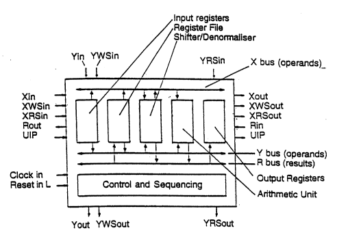
FIG. 1 is a schematic diagram of one processing elernent;
FIG. 2 is a schematic diagram of one embodiment of a systolic array
W 0 94/10638 ~ 1 ~} ~ 7 1 '~, P~r/AU93/00~73 ~
! . ~ ' .' 1
processing element chip utilising the elements of FIG. 1;
FIG. 3 is a schematic diagram of a first embodiment of a processing
apparatus utilizing the chip of FIG. 2; t
FiG. 4 is a schematic diagram of an inne~-product-step processor;
FIG. 5 is a schematic diagram of an inner-product-accumulate processor;
FIG. 6 is a schematic example of the entry of operand wavefronts to a
processor array;
FIG. 7 is a schematic example of the unloading of result wavefronts from
a processor array;
FIG. 8 is a schematic example of the entry of element-wise operand
wavefronts to a processor array;
FIG. 9 is a schematic example of the unloading of element-wise result
wavefronts from a processor array; and
FIG. 10m is a schematic diagram of a second embodiment of a processing
1 5 apparatus.
BEST MODE FOR CARRYING OUT THE INVENTION
Referring now to the drawings in detail, each processing element consists of a
number of input registers, a memory consisting of a register file and a constantROM, a shifter/normalizer, an arithmetic unit, output registers and a control and
20 sequencingunit.
~`
The datapath elements ( input registers, memory, shifter/normalizer, arithmetic
unit and output registers) are interconnected by three parallel data buses. In
addition serial interfaces are provided to and from each of the input registers
and the output register to allow communication between processing elements
25 and to facilitate construction of arbitrarily targe arrays of processing alements.
An array computes 2N2 floating point operations (1 multiply and 1 accumulate
WO94/10638 PCI'/AU)3/00573~ k~``
2 l ~ Q' 71 ~
for each processing eiement in the array) in the time taken to fetch 2N
operands. To ensure that the computation is bandwidth limited, each
processing element needs only compute at a rate of one floating p~int operation
every N data fetches. This fact leads to the conclusion that ve~ cheap
5 processing elements can be used in the array.
A schematic of the processing element is shown in FIG. 1. The choice of a `~
simple microcoded datapath and sequential algorithms to perform the floating
point operations means that the size of the processing element can be kept
small. Many such processing elements can therefore be placed on a single
10 chip. The fact that processing elements implemented in this manner are slowerthan those built using fully parallel algorithms and architectures becomes
insignificant as the size of the array is increased. This is because the
processing performance achieved is limited by the data bandwidth (and array
size), not by the computation rate for a single processing element. -~
15 The functions performed by each module in the processing element are
described below.
Input Registers: The input registers receive serial operands in the form of
{instruction, data} 2-tuples from adjacent processing elements to the left or top,
or in the case of processing elements at the top or left boundary of the array,
20 frorn operand data formatters. They then separate the instruction and reformat
the data to an internal representation consisting of separate sign, exponent andfraction words. This data is available to the processing element via the X and Yintemal data buses. The input registers also compute the sign of the product of
the two inputs, check for 7ero operand data and implement the Booth encoder
25 used during multiplication operations.
Memory: The memory consists of a Register File and a Constant ROM: The ,
register file is ~ 5 word memory used to hold the product (both fraction and
exponent), accumulator (both fraction and exponent) and temporary results. .
The product and accumulator registers can be swapped under the control of
30 microcode to facilitate efficient implementation of the pre-alignment operation in
the floating point addition and accumulation algorithms. The registers can be
loaded from the R bus, and their contents can be read from either the X or Y
buses. The Constant ROM stores a number of constants that are used during
the implementation of the floating point algorithms. These can be read via the X
W0 94/11K38 2 L ~ ,~ 7 1 ~ 00573
and Y operand data buses.
Shifter/Normalizer: Under microcode control, the shifter can either operate as ashifter (for pre-alignment of fractions before addition) or a normalizer. When
acting as a shifter, it performs right-shift operations on one operand datum (The
5 X operand). The amount by which the datum is shifted is determined by a
previously computed shift that is applied to the second input to the shifter (the Y
operand). The shifter can shift 0 to 15 bits right within one clock cycle. When
acting as a normalizer, the Shifter/Normalizer performs either a right shift by
one bit, or a left shift by 0 to 15 bits within one cycle. In this case the shift is
10 applied to the X operand input to the shifter and is independent of the Y
operand input. The value of the shift is data dependent. A right-shift is
performed if the value on the X input is the result of a computation which had
overflowed (such as in the case of addition of two normalized numbers having
the same exponent). Otherwise, a left-shift is performed. When acting as a
15 normalizer, the Shifter/Normalizer at the same time computes the offset
(exponent offset) that must be applied to the exponent of the number being
normalized in order to compensate for the shift that is applied. Shifting and
normalization operations that require shifts of greater than S1 bits can be
implemented by mulffple passes through the shifterlnormalizer.
~0 Arithmetic Unit: The arithmetic unit consists of an input multiplexer, ~n adder, a
result shifter and a flags unit. There are two parallel data inputs (X and Y) to the
arithmetic unit and a single parallel data output (R). The input multiplexer canbe used to complement and/or left-shift the X operand under control of the
Booth encoding logic contained in the input registers. This feature is used in tha
25 implementation of multiplication using a modified Booth algorithm. The
multiplexer can also be controlled directly by the processing element's
microcode to facilitate the implementation of addition, subtraction and data-
move operations.
The adder perforrns conventional two's complement addition. The carry input to ~ ;
30 the adder can be controlled by either the booth encoder logic or the processing ri
element's microcode. Both addition and subtraction can be performed by the -
combination of input-multiplexer and adder. Under control of the processing
element's microcode, the output shifter latches either the result of the
computation or the result divided by 4. This feature is used during partial
35 multiplication operations. The latched result remains valid until the next time the
WO 94/10638 . PCl`/AU93~00573 i~
2 l ~ ~ r~ ~ ~3
1 0
arithmetic unit is used. The latched result can be written onto the result bus R. ¦ -
A number of flags are set or cleared depending upon the result latched by the
arithmetic unit's output shifter. These flags include the sign of the result,
whether or not the result is zero, and whether or not the result is less than or5 equal to 15 (used to support multi-pass shifting during addition pre-alignment).
Output Registers: The output register module is used to communicate the -
results of computations back from the processing element toward the left
boundary of an array of processing elements. The output register can be ;~
parallel loaded from the arithmetic unit or can be serially loaded from a serial10 source (often the serial source is from another processing element's output
register). The output register is unloaded serially. The output register is parallel
loadable by the arithmetic unit in three parts: sign, exponent and fraction. This
facilitates conversion from the internal data representation to IEEE 754 floating
point format. -
15 During the time when the arithmetic unit is converting the accumulator contents
into IEEE floating point format, a flag is set to indicate that a register unload is
in progress (UIP).
Control and Sequencing: This module includes a microcode ROM, a program
counter, branch control logic, flags logic, an instruction register, an instruction
20 decoder, address decoders and timing and control logic. This circuitry is used to
sequence the processing element through its operations. Each clock cycle, the
microcode ROM issues a microinstruction to the processing element's datapath
units, and thereby controls the function and timing of the data operations beingperformed. Data and control flags fed to the branch control logic enable the -
25 processing element to perform data dependent operations required for
implementation of the floating point algorithms. Fields of the instruction
transmitted serially to the processing element as part of the {instruction, data}
2-tuple are also fed to the branch control logic and flags logic of the Control and
Sequencing Unit. These also determine the sequence of microinstructions
30 executed by the processing element. The instructions specified in the
{instruction, data} 2-tuple are distinct from the set of microinstructions .
implemented by the processing element The instructions specified in the
{instruction, data} 2-tuple control the flow of execution of the processing
element's microcode:
WO 94/10638 ~ ~ 4 $ ~ Pcr/Aug3/oos73
. " .
11
The intemal data representation used by the processing element uses two 32-
bit data words to represent each IEEE single precision number. One of the two
words represents the mantissa in 2's complement form, normalized to bit 29.
The second word represents the exponent using an exponent bias of 229. This
5 format provides better resolution in the mantissa than IEEE single precision
forrnat, and the use of a large exponent field virtually g~arantees that exponent
overflow cannot occur.
Within each processing element, multiplication is facilitated by the inclusion of a
modified Booth encoder and multiplexer. The denormalisation and
10 normalisation operations required by the floating point accumulation or addition
algorithms are facilitated by the repeated application of the shifter circuit which
can shift up to 15 bits in a single cycle.
FIG. 2 shows a scalable array processing chip composed of a 5 x 4 rectangular
array of single precision floating point processing elements which accept serial15 dataflow operands, and which perform a set of operations on those operands.
Each operand consists of a 5-bit instruction followed by an IEEE standard
single precision number. Each processing element is a microcoded ALU with a
; ~ 32-bit parallel datapath that includes dedicated hardware support for floating
point multiplication and addition algorithms.
20 The array of processing elements is clocked synchronously. The three bit-
serial links provide communication between processing elements. One link is
provided for each of the two input X and Y operands and one for the output, or
result operand R. As shown in FIG. 2, input data is transferred from left to right
across the array, and output results are transmitted from right to left. Chips can
25 be cascaded arbitrarily in both X and Y directions.
The operation of the scalable array processing chip is described with reference
to the system block diagram shown in FIG. 3. The data interface provides
communication between the scalable array chip and tho host system. The data
formatter elements are described separately in a co-pending application
30 number PL5696 entiUed DATA FORMATTER.
The l/O architecture of each processing element consists of two orthoganal
data transmission paths for X and Y operands, each consisting of a single one-
bit delay cell and a 32-bit data storage register. The X operand path also
WO 94/10638 PCI/AU93/00~73 ~
2 ~ 7 ~ ~
12
includes a 5 bit instruction register. Data is input to the array as a sequence of
{instruction,data} 2-tuples. These are split into separate instruction and data
words on receipt by the input registers. ~ -
Each X data operand consists of a 5-bit instruction followed by a single 32-bit ,
IEEE 754 standard floating point numben A variable length gap of several
clock periods may be present between operands for l/O synchronisation. The
operand is transrnitted in bit serial form into the processing element. When theentire {instruction, data} 2-tuple is held within the processing element, it is
cross-loaded into parallel holding registers. The instruction is decoded and
used to control the execution of the floating point algorithms. The data is
converted by hardware into the internal extended format. The internal format
has both extended precision and extended dynamic range when compared with
the IEEE standard.
The bit-serial data is bit-skewed on entry to adjacent processing elements on
the array boundary. This skew is preserved between adjacent elements within
the array by passing the data through the single-bit delay stage in each
processing element before re-transmitting it to the next processing element.
The use of serial data both rninimises the l/O pin count at the array boundary
and allows adjacent processing elements to both commence and conclude their
computations with a time differential of only one bit period. The advantage of
the bit-skewing approach over a broadcast architecture is that there is no need
to drive long buses with large buffers and thereby provides the capability for
arbitrary expansion of the array.
Bit skewing has the advantage over word-skewing in that less wavefronts are
required to complete a processing task. The bit-skewed approach therefore
results in the minimisation of job time. The computation time is minimised for
both a single job and a job stream. ,~
At the completion of a set of computations, an operand wavefront is issued to ! `
the array which causes the unloading of the results into the output registers oftheprocessingelements. ~ ~
:
Clocking of the scalable array processing chips is performed by a single phase `
50% duty cycle clock from which all intemal timing signals are generated. The
clock is buffered on entry to the chip and is distributed to each processing
W094/10638 2~ 71Q PCI/AU93/00573
13 ~ `
element. It is re-buffered within the processing element where it is used as a
locally synchronous clock. In addition, each processing element generates a
second, synchronous clock of the same frequency but with a dutyycle s
deterrnined by a self-timed circuit. The secondary clock is used to provide
timing inforrnation for bus precharging, data transfers and evaluation of
execution units.
FIG. 4 shows schematically the inner-product-step process described by Kung
and Leiserson. Data is clocked into each processing cell from the left and top
edges while the results are clocked out from right to left. For a matrix productalgorithm, an inner product accumulate aigorithm is used in preference to the
inner product step process common in much of the prior art. The inner-product
accumulate process is depicted schematically in FIG. 5. Data is again clocked
into the element from the left and top but in this case the result is formed in
place. An explicit unload phase is implementAd to obtain the result after the
computation is complete. An advantage of the inner product accurnulate
algorithm over the inner product step approach is illustrated when matrix
products are computed for matrix operands which are rectangular. The inner
product step process requires the recirculation of the result partial product
matrix. In contrast, the inner product accumulate algorithm computes the result
in-place, and incurs no hardware penalties, irrespective of the length of the ~ ;
inner products.
The sequence of operations performed by the processing elements is
deterrnined by the 5 bit instruction transmitted as part of the X operand. The
five instruction fields and their function are listed in the table below.
Instruction I BitNo. I Function
ADD 4 Floatina ~oint add
_ . . ~ -
LDR 3 Convert result to IEE format and load O/P re~ster ~-
HAD 2 Enable result unloading only if active flag set
_ _
SDE 1 Set active flaa if accumulator contents are non-zero
. r
CLR 0 Clear accumulator prior to computation
TABLE 1
i ~ l
WO 94/10638 PCI'/AU93tO0573 .~
2 1 ~ 7 ~ iJ ~
14
The default operation performed by the PE (i.e., when none of the fields of the ;
instruction are asserted) is an inner-product operation implemented as a
floating point multiply-accumulate, the input X and Y operands bein~ multiplied
and accumulated with the contents of the accumulator.
.
5 If the ~LR field is asserted, the accumulator contents is cleared before the
computation commences. This generally occurs for the first wavefront of a
matrix multiplication, and also when executing element-wise operations. The
accumulator is cleared before the computation is commenced but after the
ACTIVE flag is set if (the SDE field) is set, and after ~he accumulator has been10 unloaded into the result register (if the LDR field is set).
If the SDE field is set AND the value held in the accumulator (from the previousoperation) is non-zero, an internal flag, ACTIVE (one per processing element)
is set to indicate that this processing element is an active element. Only active
elements are permitted to unload results during element-wise operations.
15 If the HAD field is asserted, the operation being performed is deemed to be an
element-wise (hadamard) operation. If this field is set, only those processing
elements flagged as active elements (as determined by their ACTIVE flags) can ~`
unload their accumulator contents into their output register R.
If the LDR field is asserted, the accumulator contents from the previous
20 computation are converted back to IEEE format and are unloaded into the
processing element's output register.
During the unloading process, the processing element issues a flag (UIP) to
indicate that the unload is in progress.
:~ .
If the ADD field is asserted, the X and Y operands are added rather than
25 multiplied prior to the result being stored in the accumulator. The HAD and CLR
fields must also be asserted for matrix addition instructions. . ~ `
.
The element-wise operations of addition and multiplication defined by
C = A + B where cij = aij + bij
C = A B where cij = aijbij
;.; W094~10638 2 L4871 Q PCT/AU93/00573
~, . '. I .
are performed by first setting the active-element (ACTIVE) flag in a desired
processing element. This procedure is typically done once during system
initialization. It is achieved by issuing an instruction with the SDE (set active
element) field asserted. When this occurs, processing elements that contain
5 non-zero results in their accumulators set the value of their ACTIVE flag to
TRUE.
The processing elements accept operand data and return results in IEEE
standard forrnat. Internally, an extended precision format is used for both the
mantissa and exponent of the partial results.
10 The internal formats used for the representation of mantissa and exponent are as follows:
. .
2's complement mantissa sgf.ffFtfffffffffffffffffffffffff
Exponent Oeeeeeeeeeeeeeeeeeeeeeeeeeeeeeeee
Exponent Bias 001000000000000000000000000000000
~: ' ,.,
where:
s is the sign bit of the mantissa. +/ is represented as 0/1
respectively.
g is a guard bit used to avoid mantissa overflow during
accumulation.
f is a fraction (mantissa) bit. The mantissa is normalized: the most
significant fraction bit is 1 (explicit).
is the position of the binary point (showing that the mantissa is
normalized).
e is a bit of the exponent, which is held in biased form. The . ` `
exponent bias is 229.
,
If the flags in the anti-active processing elements have been set by a prior SDEinstruction, and an element-wise multiplication of a matrix A with the unit matrix
is executed, the result of the operation is the transpose of the matrix A. If anarbitrary orthogonal set of elements have their flags set, a permutation of the -
input matrix will be performed by this element-wise product.
-
When an unload (LDR) instruction is received, the accumulator contents are
converted from the internal format to an IEEE standard form. Numbers outside
WO94/10638 PCI/AU93/00573-
16
the range that can be represented by the IEEE single precision format are
truncated to zero (in the case of results with large negative exponents, including
IEEE denormali2ed numbers) or limited to infinity (in the case of nurnbers with
large positive exponents). In both cases, the sign of the zeros or infinities are
retained (unless the result is a true zero, in which case positive zero is always `
returned).
The IEEE representation of the result is loaded into a separate output register
which is concatenated with other output registers in adjacent processing
elements to form an output register chain. The result is output in a serial formthrough this register chain.
Matrix algorithms which are elements of the set of primitive operators
{multiplication, addition, element-wise tor Hadamard) multiplication,
permutation} are performed directly by the processing array. Implementation of
these operations for operands whose dimension exceeds the si e of the array `-
is possible by mathematically partitioning the operations to a set of operations ~ -
which can be computed separately using the available array size. ~`
For the particular case where the problem size does not exceed the size of the
array, recursive algorithms can be implemented which recirculate the output of
the array back to its input. This can be a useful method to minimise memory
bandwidth requirements in particular applications. -
If a matrix multiplication is commenced with an instruction which does not clearthe accumulator, the result of the multiplication will be summed with the prior
result. This gives a matrix multiplication/accumulation capability which has
direct application to the evaluation of complex matrix operations.
FIG. 6 shows the way in which conformal matrix operands are entered into the
systolic array. Bit-skewing is indicated by the small offset between adjacent ~ .
rows of A and columns of B. Each element of the processor array computes an
element cij of the result matrix C, by evaluating the inner product
Ci j--~k=o aikbkj When the last wavefront has been input to the array,
the result matrix may be read from the array. The elements are obtained in the
order shown in FIG. 7.
If the processing elements on the main diagonal in the array have their active
WO 94/10638 21 ~ 7 ~ ~, PCl~/AU93/00573 ~.. 1``-
17
element flag set by an arbitrary prior operation as shown in FIG. 8, the
processor array can be used for the element-wise operations of addition and
Hadamard multiplication. FIG. 8 shows the entry of conformal matrices to a 4 x ¦4 subarray of the chip for the purposes of element-wise addition or
5 multiplication. Only those elements shown as are used.
FIG. 9 shows the relationship between rows of data which are output from the
array after an element-wise operation. Due to the word-length registers present
in the output register chain, the data is skewed by one word-time plus one bit- ;
time. The additional bit-time delay is caused by the bit skewing of the input
1 0 operands.
-
,: ~ ...
In a second embodiment the invention has been implemented in a system -`-
hosted by a $un SPARCstation. The matrix processor is interfaced to the Sun
SPARCstation via the SBus. This arrangament is convenient since it allows the
; ~ SCAP hardware to operate using virtual addressing, with virtual to physical
translation being performed by the SBus controller in the SPARCstation. The
host processor and the matrix processor therefore share the same data space,
so both can interact with the matrix data directly. This approach does however
have its own disadvantages, the most critical being the fact that the data
transfer rate aCrQss the SBus tends to be quite low due to the overheads of
address translation. ;`
.
To compensate ~or this low data rate, the matrix processor also includes a
cache memory subsystem. The cache supports burst mode data transfers
across the SBus on cache misses and can also be used to hold frequently used
operand matrices (such as coefficient matrices in transform applications) and to25 store temporary or intermediate results.
. ~, .
A novel cache partitioning scheme has been implemented. The technique
allows the cache to be dynamically divided into a number of regions that are ;guaranteed not to interact thereby ensuring that fetches for one matrix operand ,-
do not interfere with fetches for the other. The data controllers determine how
the cache is partitioned on a per-operand/result basis (it is also possible to
assign a cache partition to the instruction streams) by issuing an 8-bit space
address along with each address generated. Each bit of the space address can
be set or cleared, or can take on the value of one of the generated address bits.
In our system implementation, three bits of this space address are used to
WO 94/10638 PCr/AU93~00573,~
21$37~
18
control non-cached accesses, tempora~ matrix accesses and temporary matrix
I -
initialization. Four bits are used to partition the cache into up-to 16 independent
regions. Use of the temporary matrix control bits of the space address allows
temporary result matrices to be stored entirely within the cache without being
written out to the host. In fact, such matrices are entirely invisible to the host ~,
processor. The maxirnum data throughput obtainable using the cache is 12.5
-
Mwords/second.
The two custom chips implemented during the development of this system are
a processing element array chip and a data controller chip. Both chips were
designed using a generic 1.2 micron double layer metal CMOS procèss rule-set
and were retargetted for fabrication using a 1.0 micron process using a gate
-
shrink.
'.
The processing element array chips are full custom integrated circuits each
~
containing an array of 4 rows by 5 columns of floating point processing
--
elements. Because the overall computation rate is limited by the available data
bandwidth, the speed of computation of the processing elements if not overly
important. Therefore, the architecture has been designed to yield processing
elements (PEs) that are physically small rather than being particularly fast.
Each complete floating point unit occupies only 2.7sq mm.
;
The processing element does not include a dedicated hardware multiplier, but
is implemented as a simple microprogrammed 32-bit datapath with hardware ~ ;
support to aid the floating point computations, as illustrated in FIG. 5.
.
The PE hardware incorporates a booth encoder and multiplexer to facilitate
multiplication using an iterative modified booth algorithm, and also a
shifter/normalizer that can be used for pre-addition alignment as well as post
addition normalization. When used as a normalizer, the shifter has the ability to
compute the amount by which the exponent must be adjusted during the same
time that the normalization occurs. Computation of the flaating point arithmetic . ~. -
operations (multiply/accumulate, multiply or add/subtract) are completed within
40 clock cycles. c
The processing element array cnip accepts IEEE single precision floating point
numbers as inputs and feeds results back through the data controllers in the
same format. Intemally, a proprietary number representation is used, including
WO 94/10638 2 ~ 7 1 (~ PCI`/AU93/00573
19
a 31 bit exponent thah~irtually eliminates the possibility of exponent overflow.
The chips operate at 20MHz clock speed, achieving around 20 MFLOPS peak
performance per chip. Processing arrays of arbitrary size can be built with no
extemal components simply by stacking thP chips to form a two dimensional ~'!" "'
5- array. The pin-out of the chip is such that 1-to-1 connection of inputs and
outputs of adjacent chips can be made. All communication to and from the
array is via the edge elements of the array. Operand data enters the array on ~
left and top edges. This data is known as the X and Y operand data ;--
respectively. The result data (R) emerges from the left edge of the array and
10 can be extracted independently from the application of operand wavefronts
(that is, the operand and result streams operate in parallel).
.....
The only global signals in the array are clock and reset. Because all
communication is local (nearest neighbour only), the system is insensitive to -
clock skew from one side of the array to the other. The only requirement is that15 the skew between adjacent PEs is kept under control. This can be readily
achieved by orderly layout of clock routing and/or insertion of clock buffering.
The processing elements are low power devices due to their architecture. The
entire chip containing 20 processing elements dissipates less than half a watt. `
This corresponds to less than 5mA per processing element at 20MHz
20 operation, or 5mA per MFLOP.
Number of Transistors 270 000
Die Size (Pad to Pad) 8.56mm x 8.35mm
Transistor Density 3800 T/sq mm ,
Power Dissipation 0.5 Watts
Packa e 68 CLCC
9 ~ .
Floatina Doint Performance 20 MFLOPS ~ 20 MHz
_ .
Design Style Full Custom ~-
TABLE 2
The perforrnance attained by the apparatus of the second embodiment for a
range of applications is shown in Table 3.
WO 94/10638 PCI'/AU~3/0057~
21~-~7`~ ~
j . .:
Application Exec. TimePerformance
3450 point 1 D Fourier transform 20 msec 130 MFLOPS
using 2D factorization A ~3 ,
2D Fourier Transform of 380380 1385 msec 66 MFLOPS
point image
4000 tap FIR Filter 35 msec per 1000210 MFLOPS `
data samDles . .
. . -:
1 0th order Matrix polynomial 136 msec 114 MFLOPS
evaluation of 60 x 60 complex ..
matrix
QR factorization of 59 x 60 Matrix 561 msec 87 MFLOPS
TABLE 3
~ `:
ii~