Note: Descriptions are shown in the official language in which they were submitted.
2~
!"
i .: 1 21~g81 1 PCT/US93/10677 '~:
., .
.:, .
''VIOEO PROCESSING ~IARDWARE
:.` g
. ,~
S Field of the Invention
`:This invention relates to a system of programrnable logic devices ~PLDs) for
implementing a program which tradi~onally has been software implemented on a
.~general purpose computer but now can be irnplemented in hardware. This inven~on
., .
;`~also relates to a method of ~anslating a source code prograrn in an algorithmic
~10 language into a hardware description suitable for rumling on one or more
programmable logic devices.
Background of the Invention
The general purpose computer was developed by at least the 1940s as the
,;~15 ENL~C machine at the University of Illinois. Numerous developments lead tosemiconductor-based computers, then cen~ral-processing units (CPUs) on a chip such
`~as the early InteI 4040 or the more recent.lntel 486, Motorola 68040, AMD 29000, -
and many other CPUs. A general purpose computer is designed to implement
instructions one at a time according to a program loaded into the CPU or, more
~0 often~ available in connected memory, usually some form of random access memory
A circuit specifically designed to process selected inputs and outputs can be
designed to be much faster than a general purpose computer when processing the
same inputs and ou~puts. Many products made today inc.lude an applica~on specific
~5 integrated circuit (ASIC) which is optin~ized for a particular application. Such a
. , .
circuit cannot be used for other applications, however, and it requires considerable
expense and effort to design and build an ASIC.
'~To design a typic~l ASIC, an engineer begins with a speciIScahon which Jt~ -
~0 includes what the circuit should do, what I/O is avaiIable and what processiI?g is
required. An engineer must develop a design, progr~n, flow chart, or logic ~low and
`then design a circuit to im,plement the specification. This typically involves (1)
yzing the internal logic of the design, (2) conver~ing the logic to Boole~
`! `
.,
~;
.,
i "
wo g4/l0624 2 1 4 8 8 1 ~ 2 - PCr/lJS93/10677
`; functions which can be implemented in hardware logic blocks, (3) developing a
i~ schematic diagram and net list to configure and connect the logic blocks, then (4)
~; ~
implementing the circuit. There are a number of computerized tools available to -
~` assist an engineer with this process, including simulation of por~ons or all of a ~
S design, designing and checking schematics and netlists, and laying out the final ASIC,
typically a VLSI device. Finally, a semiconductor device is created and ~he part can
be tested. If the part does not perfonn as expected or if the specification changes,
~-~ some or all of this process must be repeaoed and a new, revised ASIC must be
designed and created until an acceptable part can be made which meets or
`~0 approx~mates the specification. The entire design process is very time consurr~ing and
requires the efforts of several engineers and assistants. It is difficult to predict
exactly what the final part will do once it is finally manufactured and if the part does
~; not perform as expected, a new part must be designed and manufac~lred, requiring
~ more time, resources and money.
5~ There are several alternabves to ASlCs which may provide a solution when
balancing cost, number of units to be made, performance, and other considera~ions.
Field Prograrnmable Gate Arrays (FPGAs) are high density ASICs that provide a
J number of logic resources but are designed to be configurable by a user. FPGAs can
.0 be configured in a short amount of time and provide faster perfonnance than ag0neral p~rpose computer, although generally not as fas~ as a ~lly customized circuit,
~;~ and are available at moderate cost. ~PGAs can be manufac~red in high volume,reducing cost, since each user can select a unique configuration to run on the standard
FPGA. The configuration of a part can be changed repeatedly, alIowing for rminor or
?~ ~5 even total revisions and specification changes. Other advantages of a configurable,
stand~rd part are: faster ~rne implement a speci~ca~on and deliver a func~ional unit
y to market, lower inventory risksiJ easy design changes, fasiter delivery, and
availability of second sources. The prog~mmable nattlre of the FPGA allows a , `
:~ i finished, commercial product to be revised in the field to incorporate improvements ,~ .
;, !
O or enhançements to the specffica~on or finished product.
,",~:'.,1
~. '
WO 94/10624 ~ 3 ~ 2 1 4 ~ 8 1 ~ Pcl/US93/10677
A gate array al1Ows higher gate densities than an FPGA plus custom circuit
design o~tions but requires that the user design a custom interconnection for ~he gate
array and requires manufacturing a unique part and may require one or more
revisions if the specification was not right or if it changes. The user must design or
` 5 obtain masks for a small number of layers which are fabricated on top of a standard ,
gate array. The cost is less th~n for fillly custom ICs or standard cell devices.
.
One significant development in circuit design is a series of
J programmable logic devices (PLDs) such as the ~ilinx XC3000 Logic Cell Array
I 10 Family. Other manufacturers are beginning to make other programmable logic
devices which off~r similar resources and functionality. A typical device includes
many configurable logic blocks (CLBs) each of which can be configured to apply
selected Boolean functions to the available inputs and outputs. One type of CLB
includes five logic inputs, a direct data-in line, clock lines, reset, and two outputs.
` 15 The device also includes input/output blocks, each of which can be configured
independently to be an input, an output, or a bidirectional chamlel with three-state
control. Typically, each or even every pin on the device is connected to such an I/O
block, allowing considerable flexibility. Finally, the device is rich in interconnect
lines, allowing alrnost any two pins on ~he chip to be connected. Any of these lines
, 20 can be connected elsewhere on the device, allowing sigr~ificant flexibili~y. Modern
devices such as the Xilinx XC 3000 series include the XC 3020 with 2000 gates
through the XC 3090 9,000 gates. The XC 4000 series includes the XC 4020 with
20,000 gates.
To aid the designer, Xilinx can provide software to convert the output of a
circuit simulator or schema~c editor into Xilinx netlist file (XNF) cornrnands which in
turn can be loaded onto the E~PGA to configure it. The ~ypi~l input for the design is
a schematic editor, including standard CAE so~tware such as futureNet, Schema, ;~;:
OrCAD, VIEWlogic, Mentor or Yalid. X~ provides programrnable gate array
libraries to permit design entry using Boolean equa~ons or standard TTL funchons.
Xilinx design implementa~on software conver~s schemahc netlists and Boolean
equations into efficient designs for prograrnn~ble gate arrays. Xilinx also provides
~, I
WO 94/10624 2 1 ~ g ~ 1 4 PCI/US93/10677
i; verification tools to allow simulation, in-circuit design verification and tes~ng on an
l'``:;
actual, operahng part.
There are several hardware description languages which can be used to design
or configure PALs, PLAs or FPGAs. Two such languages are HDL and ABLE.
..~,;
i i, Cross-co~pilers are available to convert PALASM, HDL or ABLE code into XNF or
into code suitable for conlSguring other manufacturer's devices.
An enormous quan~ty of software is available today to run on general purpose
computers. ~ssen~ally all of that software was originally created in a high level
language such as C, PASCAL, COBOL or FORT~AN. A compiler can ~anslate
instructions in a high level language into machine code that will run on a specified
`;, general purpose computer or class of computers. To date, no one has developed a
method of transla~ng software-oriented ~anguages to run as a hardware configuration
~j 15 on an FPG~ or in ~act on any other hardware-based device.
x: ~
Other recent products have been introduced by Ap~x, Mentor Graphics and
Quick~rn. See Mohsen, USPN 5,077,451 (assigned to Aptix Corporaaon), B~tts, et
al., USPN 5,036,473 ~assigned to Mentor Graphics Corporation), and Sample et al,- ~ 20 USPN 5,109,353 (assigned to Quickturn Systems~ IncoIpor~ted). These referenGes
provide backgrt)und for the present inven~ion and related technologies.
Others have attempted to par~on logical func~ons over mul~ple PLDs but
~J these effo~ts have not provided a true, full func~on implementa~on of algorithmic
` ~25 source code. McDermith e~ al, USPN 5,140,526 (assigned to MinG 1nCOrPQrated),
describe an automated sy~em ~or par~tioning a set of Boolean logic equations onto
j~ PLDs by comparing what resources are required to implement the logic equations
with information on what PLD devices are comrnercially available that have the ' -
capabi~ity to implement the logic equ~ions, then evalua~ng the cost of any op~iO~
solutions. The disclosure focuses on par~ selechon and d3es not disclose how logic is
ac~a~y to be par~tioned across mul~ple devices.
~'
WO94~ 4 ~- 21~881~ PCI/US93/1~677
A computer program typically includes data gathering, data comparison and
data output s~eps, of~en with many branch points. The principles of programming are
well hlown in the art. A programmer usually begins with a high level perspective on
i, what a program should do and how it should execute the program. The programmer
' 5 must consider what machine will run the program and how to convert the desired
program from an idea in the programrner's head to ~ functional program running on
the target machine. Ultirnately, a typical program on a general purpose computer is
~, written in or converted by a compiler to n~achine code.
~!
dO A prograrnsner will usually write in a high ;evel language to facilitate
~il organ~zing and coding the program. Using a high level language like the C language,
a programmer can control almost any function of the computer. This control is
limited, however, to operations accessible by the computer. In addition, the
programmer must work within the cons~a~nts of the physical system and generally
~15 cannot add to, remove or alter the configuration of computer components, the`~ resources available, how the resources are connected, or other physical a~ibutes of
the computer.
~, In contrast, a special purpose computer can be designed to provide specific
:-'20 results for a range of expected inputs. Examples include controllers for household
appliances, automobile systems con~ol, and sophisticated industrial applications.
Many such special purpose computers are designed into a wide range of commercialproducts, generally based on an ASIC. Programs~g an ASIC begins with a high
level description of ~e prog~am, but the prograrn must be implemented by selec~ng a
~2~ senes of gates and circuits to achieve ~e p~ograrruner's goals. This usually involves
`Ii converting the high level description into a logical desc~iption which can be
~nplemented in hardware. Many values are handled as specific signals which
typically originate in one circuit then are carried by a "wire" to another circuit where
the ~forma~on uill be used. A typical signal is created to provide for a single
~130 logical event or combina~on which rnay never or rarely occur in real life, but must
~".~ .
be considered and provided for. Eaeh such signal must be designed into the ASIC as
one or several gates and connec~ons. A complex program rnay require many such
,.,' i~ .
~`.` WO 94/tO624 21 i ~ 81~ - 6 - PCI/US93/10677
~; signals, and can consume a large portion of valuable, avail~ble circuit area and
, resources. A reconfigurable device could a~locate resources for signals only as
~:~ needed or when there is a high probability that the signal will be needed, dramatically
" i reducing the resources that must be cornmitted to a device. -~
S ~.
Progr~nming a typical ASIC circuit is not easy but there are many tools
available to help a programrner design and implement a circuit. Most programmersi use silicon compilers, computer assisted engineering tools to design schernatics which
will perform the desired functions. An ASIC must be built to be tested, although~1 10 rnany parts can be simulated with some accuracy. Almost any ASIC design requires
i, revisions, which means making more parts, which is time consurl~ing and expensive.
A reconfigurable equivalent part can be incorporated in a design, tested, and modified
-' without no or n~in~rnal modifications to physical hardware, essentially elimirlating
' manufacturing revision costs in desigr~ing special purpose computers. Current
r ,' 15 configurable devices, however, are severely limited in capacity and cannot be used
;, for complex applications.
;' A part can be simulated in hardware using PLDs, described above in the
background section. These, however, can only be effectively programmed using
hardware description langua~es, which have many shortcomings. Un~l now, there
has been no way to convert a program of any significant complexity from a high level
software l~nguage like C to a direct ha~dware implementa~on.
Summary of the In~ention
The present invention provides a video processing module designed f~ high
per~ormance using economical components. A programsnable logic device (PLD) is
conigured to modify a data stream, in par~cular a video s~eam. The PLD can be
connected to a memory resource. In addition, ~he PLD can be connected to a second
PLD through an interruptable connecaon. The second PLD can be optimized for bus
inter~ace communic~on and connected to an external system, typically a host
computer. The second PLD can take commands from the host to prepare a processLngconfiguraùon for ~e first ~LD and can connec~ when needed to download a
~ ~ WO 94/l0624 ~ 7 ~ 21 ~ ~ 81~ PCr/US93/10677
.. ,.. ~ . 1
~` configuration to the first PLD through the interruptable connection. An array of
these modules can be connected in a systolic array to provide powerf~ll, pipelined
video processing.
: ,j
The present invention provides a video processing module designed for high
`, performance using economical components. A progr~nrnable logic device (PLD) is
configured to modify a data stream, in particular a video stream. The PLD can beconnected to a memory resource. ~n addition, the PLD can be connected to a second
PLD through an interruptable connection. The second PLD can be optimized for businterface comrnunication and connected to an external system, typically a host
computer. The second PLI~ can take commands from the host to prepare a processing
configuration for the first PLD and can connect when needed to download a
configuration to the first PLD through the interruptable connection. An array ofthese modules can be connected in a systolic array to provide powerful, pipelined
video processing.
', 1
The present invention provides a configurable hiardwiare system for
" JI imp1emenhng an algorithrnic language program, including a programmable logic
:~ device (PLD), a hardware resource connec~ble to the PLD, a means for configuring
~i 20 the PLD, and a programmab~e connec~on to the PLD. The programmable
., lj
connection is typically an I/O bus connec~ble to ~e PLD. The PLD may include an
and/or mah-Llc device or a gate array, that is, a prog~ble array logic (PAL3
~`3, device and a gate array logic (GAL) device. The hardware resouree may be a DSP,
~li a memory device, or a CPU. The hardware system is designed $o provide resources
,~ 25 which can be configured to implement some or all of an algorithmic language
program. These resources can be placed on a module, referred to herein as a
~i ! distributed processing unit ~DPU).
'
One example of an algorithmic program is the classic 'IHello, World!" C
30 program. This program could easily be modified to output that famous message to a~
LED readout only when prompted by user ~nput or perhaps to repeat that message at
,~I!;i'
selected timcs without input or promp~ng. Another example of an algorithmic
?,".,iij
~i
~0 94/t0624 2 1 ~ 8 8 1 4 Pcr/uss3/lo677 ~ ~
' '
.1 ' ' ' ' '~.
program is a digital filter which modifies an input data stream such as a sound or
, videosignal.
!
'~ A larger system can be built to make an extensible processing unit (EPU~from
. S multiple DPUs plus support modules. A typical DPU includes a PLD3 a hardwareresource connected to t.he PL~, a means for comSguring the PLD, and programmable~, connections to the PLD. The programmable connections are ~pically an I/O bus. In
addition, a typi~l EPU will include one or more dedicated bus lines as a
configuration bus, us~ to carry configuration information over the configuration bus.
.'~ 10
., .
One useful DPU is a VideoMod (Vmod) for processing video informa~on. A
Vmod may be op~r~ized for real ~ne processing of an active video stream or may be
optimized for off-screen processing.
~I Each module in an EPU can be connected to other modules by one or more of
several buses. A neighbor bus ~N-bus) connects a module to its nearest nelghbor,typically to ~he side or top or bottom in a two dimensional wiring array. A module
bus (M-bus) connects a group of modules, typically two to eight modules, in a single
~ 20 bus. A host bus (H-bus) connects a module to a host CPU, if present. A local bus
i
i a,-bus) connects components within a single module.
~,,
The invsn~aon also irlcludes a method of t~anslating source code in an
algorithmic language into a configuration file for implementation on a processing
25 device which supports execu~on in place. This is par~cularly usef~l for use with ~e
modules described above, including PLDs connected to a hardware device such as aDSP, CPU or memory. The PLD can be comlected to a device capable of processing
digital instruc~ons. The algorithmic language can be essen~ally any such language, ~ -
but C is a preferred algorithmic language for use with this invenhon. ~-
The method includes four sequen~al phases of translation, a tokenizing phase,
a logical m~pping phase, a logic op~niza~ion phase, and a device specific mapping
WO94/10624 ~ 21 ~g,5,~1 l Pcr/Us93/10677 1'`
phase. One embod~nent of the method includes transla~ng source code instructions~, selected from the group consisting of a C operator such as a mathematical or logical
` `1 operator, a C expression, a thread control instruction, an I/O control instruction, and
a hardware implementation instruction. The translator includes a stream splitter,
`~ S which selects source code which can be implemented on an available processing
. device and source code which should be i~nplemented on a host computer connected
.~ to the processing unit. The hardware implernentation instructions can include pin
assignments, handling configurable I/O buses, commun~ca~on protocols between
~, devices, clock generation, and host/module I/O.
: " j
One object of the invention is to provide a high speed video processor.
~1 .
Another object of this invention is to provide a systolic array of PLDs for
video processing.
~ 15
Another object of this invention is to provide hardware resources to implement
an algorithrnic software program in hardware.
Another object of S~his invention is to provide a syste~ and method dlat can
20 implement in hardware an algorithmic software program for video processing
'.~! 1
One object of the invention is ~o provide a high speed video processor.
~ .
`"' ! Another object of this inven~ion is to provide a systolic alTay of PLDs for
video processing.
Another object of this invention is to provide hardware resources to implement
an algorithmic software program in hardware. ~,
Another object of dlis invenhon is to provide a system and method that can
implement in hardware an algori~hmic so~tware progr~un for video processirlg.
~`'' .
WO 94/10624 21~ ~ 81~ - 10 - PCJ/US93/10677
`, Anothe~ object of this invenhon is to provide a stream splitter to analyze an ',
., ,
algorithmic source program and implement as much of the prograrn as possible on the
available hardware resources.
.. ..
S Yet another object of this invention is to provide hardware resources which
~, can be reconfigured in whole or in part in a relatively short tirne to allow swapping
of computer ins~uctions. ,This allows a sLngle set of hardware resources to
~'~ ~rnplement many di~ferent computer programs or a large program on limited
.`~ resources.
` 10
:, Brief Description of the Draw~gs
Figure 1 illustrates one embodiment of a module of this invention, in DIP
package forrnat.
Figure 2 illustrates a second embodiment of a module of this inven~on, in
15 SIMM module format.
Figure 3 illust~ates a PLD connected to an N-bus, M-bus and L-bus.
Figure 4 iLlustrates the logic symbol and main connections to a DPU.
Figure 5 illustrates a module with multiple DRAMs connected to a PLD.
Figure 6 illus~ates a module with mu~ple DSP ur~its connected to a PLD.
Figure 7 illustrates a different module including DSP units connected to a
PLD.
Figure 8 iLlustrates a bndge module.
Figure 9 illus~ates a repeater module.
Figure lO illustrates an extensible processing unit and the interconnections
~!~ 25 between dis~ibuted processing units. ,
Figure l l illustMtes one pinout conhgura~on of a DPU.
Figure 12 illustrates a logic symbol for an EPU.
Figure 13 illustrates one embodiment of an EPU assembled on a PC board and
3 connected to an ISA bus inter~ace. -
Figure 14 illustrates another embodiment of an EPU assemble~ on a PC board
and connected to an ISA bus interface.
~:.
.
,~. 1
,;, .
... .
i -;
WO 94t20624 - 1 t 1 ~ ~ 8`1 4 P~/US93/10677
. . .
Figure 15 illus~ates an embodirnent of an EPU wi~h two bridgemods, each
`, conneeted to a comm,on SCSI interface plus an alternate DPU configuration.
Figure 16 illustrates sever~ different configura~ions of buses.
Figure 17 illustrates ~e components and process of stream splitting.
S Figure 18 illustrates the locahon of many code elements after using the stream
. splitter.
Figure 19 illustrates program flow of an algorithmic source code program
~ before and after applying the stream splitter.
`~l Figure 20 illus~rates ~e program code resident on the hc,st before and after
i 10 applying the stream splitter.
Figure 21 illustrates rnajor elements of the steam splitter libraries and
,1, applications.
Figure 22 illustrates the locahon an,d program/hrne flow for a program running
on several modules without stream splitting.
Figure 23, illustrates the location and program/~e flow for the same program
split to run on three modules and ~e host.
~`Z Figure 24 illustrates emulation of the "C" programming l~nguage in PLDs.
.~j
;~1 Figure 25 illustrates several representahons of flow through opera~ons
~iif ~mplemented in DPUs.
Figure 26 illustrates several representa~ons of state operations implemented in
DPUs.
Figure 27 illus~ates implementation in an DPU of execu~on domains.
Figure 28 illustrates implementa~on in an DPU of condi~onal statements.
Figure 29 illustrates implementa~on ~ an DPU of a conditional (while)
loop and a for loop.
.;,
Figure 30 illus~ates implementation in an DPU of a func~on call and fimchon
defini~nn.
Figure 31 illustrates a "C" program implemented in a PLD and shows the state
o~ the system at several ~nes.
Figure 32 illus~ates a general design ~or a Video processing module or Vmod.
``` Figure 33 illusb~ates a basic Vmod ~or video stream processing.
... .
~' Figure 34 illus~ates a Ymod with two source s~eams and a history ~l~O.
. .
.;,
,
~,,," :
;.....
~` W094/10/i24 ~1~8814 - 12- PCI/US93/11~677 i~
Figure 36 iUustrates a Vmod using a FIFO for input selechon. l-
Figure 37 illustrates a Vmod with write-back to a frame buffer.
Figure 38 illustrates a Vmod with SRAM connected to the FPGA for real-time
filter~ng.
S Figure 39 illushates a Vmod for processing of multiple video frames.
Figure 40 illustrates a Vmod for copy~ng frames.
. Figure 41 illustrates a Vmod for memory mapping.
Figure 42 illus~ates a Vmod for n~ixing inputs from FPGA and video stream
sources.
Figure 43 illustrates another Vmod for mi~ng inputs from FPGA and video
stream sources.
Figure 44 illus~ates another Vmod, also referred to as an rtDSPMOD.
Figure 45 illustrates a system connec~ng eight rtDSPMODs.
Figure 46 illustrates a second system connec~g eight r~DSPMODs.
~15
Detailed Description of the Preferred Embodi~nents
The present inven~on is designed to provide hardware resources to implement
algorithmic language computer programs in a specially configured hardware
environment. The invention has been developed around the Xilinx XC 3030 field
20 prog~able gate array ~FPGA) but o~her Xilinx parts would work equally well~ as
would similar parts from other manufacturers. A PLD typically contains configurable
logic elements plus input and output blocks and usually ~ncludes some simple connect
paths, allowing implementa~on of a variet,v of state machines or a simple reroutable
~J bus.
~25
s; ~l
`i~ The simplest implementa~on of the device of this invenhon is a combina~on of
~ j i
' a prograrrunable logic device (PLD~, a hardware resource, a means ~or configuring
''~ the PLD and a programmable connection to the PID. Re~ernng to Figure lA, PLD i~
,.. . .
1 11 is connected to a hardware resource, DRAM 13, through one or more address
i 30 lines 18A, one or more con~ol lines 18C~, and one or more data lines 18D. One
means for configuring PLD 11 is from comSguraaon d~ta stored in EPROM 12
through EPROM interface lines 19A and l9B. Alterna~vely, configura~on data can
~'
~.?:,
W O 94/10624 - 13 - 21 ~ ~ 81 ~ PCT/US93/10677
be loaded through onè or more user I/O lines 17 EPROM 12 can con~in data or
other information useable by the PLD once it is configured. EPROM 12 can also
contain data for multiple configurations. These devices c~n be assembled as a single
~i module, e.g. distributed processing unit ~DPU) 10. ~eferring toFigures lB, 1~ and
lD, one embodiment of DPU l0 consists of cærier 15 with traces (not shown)
connecting one or more EPROMS, e.g. EPROMS 12A and 12B, to PLD 11 and
other traces connec~ng one or more DRAMs, e.g. DRAMs 13A through 13D, to
'I
PLD 11. Additional traces connect user I/O lines 17 between PLD 11 and pins 16 on
the edge of carrier 15. Pins 16 can be connected to external circuitry with I/O lines,
~10 power, clock and other system signals, if needed. PLD l1, EPROM 12 and DRAM
13 can be connected to carrier lS by surface mounting, using a chip carrier, or using
~Iq other techniques well known in the art. It is also possible to implement the entire
` DPU 10 on a single semiconductor substrate with programmable interconnect linl~n
PLD, EPROM and DRAM blocks.
A basic configuraaon rou~ne can be stored in EPROM 12 so that when ~e
device is first powered up, EPROM 12 will load an ~n~tial logic configuration into
PLD 11. I/O pins on PLD 11 for lines 17 and 18 are allocated and protocols for
using those lines are pre-defined and stored in EPROM 12 then loaded from EPROM
12 into PLD 11 when DPU l0 is first powered up and configured. At least one line19 between EPROM 12 (if present) or user IIO line 17 (if no EPROM present) is
permanently configured in order to load initial configuration data. Data flows within
, DPU 10 vh I/O lines 18 and 19 and may be buffered in DRAM 13. Data exchange
with external devices flows over lines 17. DRAM 13 can be used to store
25 inforrnation from EPROM 12, to store interrnediate results needed for opera~on of
the program Oll PLD 11, to store informa~ion from user I/O lines 17, or to store
. . .
~i o~er data required for operation of DPU 10. Operators and variables, as needed for
`~1 program func~on, are loaded as~ part of dle configuration data in PLD 11. The
sequencing of program steps does not necessarily follow the traditional von Neumann
30 structure, as described below, but results from operation of DPU 10 according to the
configuration of PLD 11 and the state of ~e sys~m, including relevant inputs and
~;~
'.. '1 ,
L,.
`''I ~.:` -.
WO 94/10624 _ 14 - PCI/US93/10677 ~:
214~8~
~` outputs. Configurat:~on data is reloadable according to the source program and
current task and application requirements.
.~
.
In a preferred embodlment, data for several configurations is precalculated and
,`1 5 stored so as to be conveniently loadable into Pl D 11. For example, EPROM 12 may
contain data for one or more configurations or partial configurations. DRAM 13 car
``~ be used to store configuration data. If, during execu~on of a program on PLD 11, a
jump or other instruction requires loading of a di~ferent configuration, the data for the
new configuration or partial configurahon can be rapidly loaded and execuaon cancontinue.
A sirnple device configuration might be used as a special purpose mformation
processor. One or more of user IIO lines 17 can be connected to a sirnple input
device such as a keyboard or perhaps a sensor of some sort (not shown). One or
more other user I/O lines 17 can be connected to a simple output device such as an
indicator light or an LED numeric display (not shown~.
Alternatively, a DPU can be prepared in a preconfigured and consistent
modular package with assigned pins ~or power, programrn~g, program data, reset,
system control signals such as clock, and buses for use with the system. In a
~'.'.;2'' preferred embodiment, a DPU is a module with 84 pins and 3 configurable buses,
~, with 20 pins for each configurable bus and 34 pins for the remaining functions.
lReferring to Figures 2A through 2D, the DPU is built on a standard 84-pin SIMM
;` board 20j 134 mm wide, 40 mm high, and 1 millimeter thick, with edge connectors
21 for cormec~on to socket 22 in connector 22A (Figure 2C). Loc~ng pins 24
engage holes 23 to hold board 20 firmly in socket 22. Referring to Pigure 2C, board
20 can be connected to a corresponding socket such as AMP822021-5. Board 20 can ,~
hold up to four devices 25 on one side. Each device 2;, preferably 33 x 33 mm,
may be a DSP, a PLD, EPROM or other device. In one preferred embodiment, each
~ 30 device 25 is a DSP such as an Analog Devices AD 2105, AD 2101 or AD 2115. Irl <
,~,,,~!"~ another preferred embodiment, each device 25 is a PLD such as a Xilinx XC4003.
Board 20 can hold PLD 11 and DRAM 27 on the other side. In a preferred
~i
,lj.,
WO 94/10624 _ 15 - 21 1~ PCI/US93/10677
embodiment, PLD ll is a Xilinx XC4003, 33 x 33 mm, coupled to eight 4 Megabit
D~AM 27 memory chips. In another preferred embodiment, PLD ll is a Xilinx
3030. The devices ca l be surface mounted to mil~imi~e overall size. Refe~ring to
j Figure 2D, board 20 is about 1-2 msn thick, and DRAM 27 is about l snrn thick~and
`~ S Pl.D 11 is about 5 mrn thick, giving an overa}l thickness of about 7-8 mm. The
.. j~ ..
~ ~, overall space erlvelope ~or a fully loaded board 20 is less than 135 by 40 by 8 mm.
. .
Sockets are designed on 0.4" (lO.l rnm) pitch.
~j ~eferring to Figure 3, PLD 11 together with DRAM 13 and the connecting
0 wiring are part of DPU ~3. PLD 11 contains one or more configurable logic blocks
,;~ 30, e.g. 30A, 30B, one or more configurable I/O ports including neighbor bus ~-
"I
bus) con~ol port 31, program control port 32, address generator 33, and D~AM
'i control 35, and other portions such as X-bus I/O control 34, X-bus 37 connected to
tristate buffèrs 36A, 36B, and power circuits 38. The X-bus is an arbi~rary bus that
provides a means to pass signals through PLD 11 without modifying them. PLD 11
is comnected to DRAM 13 through prograrnrnabIe interconnect which can be
~i reconfigured as needed to complete ~e interface. The specific pins on PLD 11 that
~ carry signals to Dl~AM 13 can be reconfigured as needed. Typically the wires that
,~,,,~
``!, actually connect PLD l1 arld D~ 13 are fixed M place, but the function of each
~0 wire can be reconfigured as long as both PLD 11 and DRAM 13 have configurable
inputs. PLD 11 has reconfigurable ~nput and output pins~ DRAM 13 can be
P ! manufactured with reconfigurable inputs and outputs, although at present there are no
such devices on the market. PI,D 11 s~ll may be reconfigured to interact with a
' 1 variety of DRAM devices which may have differing pin functions and pin~`2~ assignments. Address generator 33 is connected through one or more (typi~lly lO~
address (ADDR) lines 53 to address circuits in DRAM 13. X-bus 37 is cormected
~rough tristate buffer 36B through one or more data lines 54 to data circuits in ' ~
J~ DRAM 13. DRAM control 3~ is eonnected through one or more RAM control ~ -
; (RAM^C) lines ~5 to RAS and CAS circuits in DRAM 13 and through one or more
bus control (13US-C) lines 56 to read and wlite circuits in DRAM 13.
,. .; . ,
.
~"
~r~
WO94/10624 21~14 16 - PCI/USs3/10677
Pl D 11 is co~nected through several configurable lines to the rest of the
~ system, represented here by connect block 47. N-bus control port 31 is connected to
'i' one or more lines which ~orm neighbor bus ~N-bus) 49. X-bus 37 is connected
through tristate buffer 36A to one or more lines which form module bus (M-bus) 50.
Program control port 32 is connected through one or more lines 51 to prograrn -
circuits in connect block 47. In some applications, the program control lines will be
fixed and not reconfigurable and provide a means of loading initial configuration or
program information into PLD ll. Power circuits are connected to power circuits
through one or more lines 52. In most applications, power lines 52 would not be
~1 1O reconfigurable and would be hard wired to serve a single function.
~, ~ , .
N-bus 49 provides global connectiviq to the closest neighboring DPU
~`, modules, as described belqw, allowing data to flow through a systolic array of
processors. M-bus S0 provides connectivity within a group of DPUs, as described
below, which typically extends beyond ~imrnediate neighbors.
One or more lines form ~L-bus 58 which connects PLD 11 through I/O circuits
~not shown) to other PLDs or other devices, generally mounted in the same DPU.
:J,~ The L-bus allows multiple PLDs in a single DPU to implement Boolean logic that
will not fit on a single PLD. N-bus 49, M-bus 50 and L-bus 58 a~e configurable into
an arbitrary number of channels, with arbitrary protocols. The total number of
~lt.
channels in any bus is limited by the to~al number of lines allocated to that bus but
one skilled in the art will recognize man~ ways to allocate total lines among several
buses.
~25
Referring to Figure 4,~ a DPU can be represented by a logic symbol with
..~,
connections to power 52A, 52B, bidirectional buses M-bus 50, N-bus 49, H-bus 59,and generally unidirectional lines prograrn 51A, prograrn data 51C, reset 51B, and
cloclc 51D.
~30
..
i.~ .
~ .
WO ~4/106~4 - 17 _ 2~ ~ S81 4 PCr/US93/10677 1 .
i j With Lhese basic design considerations in mind, one slcilled in the art will
;
;`, recogni~e that man,y combinations of useful components can be assembled using the
teachings of this invenhon. Re~e~ing to Figure 5, a PGA-Mod distributed prccessing
~:l module 80 may consist of carrier 15 ~igure lB) orpreferably board 20 ~igur~ 2A)
fitted w~th, PLD 11 as an ~nter~ace device connected together ~vith DSP 28 and one or ~,
.i~ more PLDs 25 through local bus 58. Each PLD ~5 is connected to each adjacent
PLD 25 through local-neighbor bus 61 and to local DRAM 27 by bus 62. PLD 11 is
s also connected to N-bus 4~ and M-bus 50. Buses N-bus 49, M-bus 50 and L-bus 58
.:1 may each be one or more lines, preferably 20. In one preferred embodiment,
~,
IO interface PLD 11 is an ~C3042-70, each of four PLDs 25 are an XC4003-6, each of
four DRAMs 27 may be 256 KB, 512 KB, 1 MB or, preferably, 4 MB, and DSP 28
i is an Analog Devices AD 2105, a lO MIP part, or AD 2101 or AD 2115, operating
at up to 25 MIPs. Faster parts or parts with more resources can be substituted as
-~, . needed.
~ 1, 15
` :, Another useful embodiment includes multiple DSP chips to provide a scalable
intelligent image module (SIImod). Referring to Figure 6, SILmod 80A is a DPU
where PLD 11 is connec~ed to N-bus 49 and M-bus ~0, to DRAM 13 through one or
.' more, preferably ten, address lines 53, one or more, preferably sixteen, data lin,es 54,
`` 20 one or more, preferably two, l~AM-C lines 55 ~connected to RAS, CAS circuits in
.,
~3, D~M 13), and one or more, preferably two, BUS-C bus control lines 56 (connected
to read/write circuits in DRAM 13), plus one or more, preferably ten, lines forming
I serial bus (S-bus) 67. Each bus line of 53, 54, 55, iand 67 is bidirectional in this
implementation except DRAM 13 does not drive ADDR bus lines ~3 or BUS-C lines
~, 25 56. A unidirectional bus is ~ndicated in Figure 6 by an arrow head, a bidirec~onal
` bus has no arrows. PLD 11 is connected to one or more DSPs 25 ~ough address
'~ lines ~3, dlata lines 54, and BUS-C bus control lines 56, plus one or more, preferably
. four, bus request lines 64, one or more, preferably four, bus grant lines 65, vne or
more, p~eferably two, reset/interrupt request lines 66 and S-bus 67. DSPs 25 are~`. 30 allocated access to internal bus lines 53, 54, 56 using a token passing scheme, and
give up bus access by passirlg a t~ken to another DSP or simply by not using the bus.
~t
~ ` `.
0624 2 1 ~ ~ 8 1 ~ PCI/US93/10677
In one preferred embodiment, PLD 11 is an XC3042, DRAM 13 includes 4-8 MB of
~, memory, and each DSP 25 is an Analog Devices AD 2105. S-bus 67 is configured
1 to access the serial ports of each device in SIIrr,od 80A and is particularly useful for
;, debugging. DSPs 25 c~, access DRAM 13 in page mode or in static column m,ode.
; 1
~ S PLD 11 handles refresh for Dl~AM 13. The dimensions of each of bus lines ~3, 54,
;~ 56 are configurable and the protocols can be Fevised depending on the configuration
and programming of each part and to meet the requirements of the dataflow, data
t~pe or types, and functions of any application prograun running on the module.
~10 Another useful embodiment includes an array of eight DSPs to provide a
DSPm~ efer~ng to Figure 7, DSPmod 80E is a DPU where PLD 11 is connected
to N-bus 49 and M-bus 50, through buses equivalent to those in SIIm~, 80A,
including address lines 53, data lines 54, and BUS-C bus control lines 56, plus S-bus
67, reset/interrupt request lines 66 and, preferably one line for each DSP 25, bus
;115 request lines 64 and bus grant lines 65. The DSPm,~d differs from a SIImod
principally in that the DSPmod does not include DRAM 13. PLD 11 can include
'r memory resources to boot DSPs 25, such as an EPROM 12 ~not shown) or
configuration data loaded into PLD 11 from an exterllal location ~not showll). S-bus
67 can be configured to transfer data to and from DSPs 25 at 1 megaByte per second
;~¦ 20 per DSP. The S-bus is prirna~ily included as another means to selectively access a
specific DSP, particularly for debugging a new protocol or algorithrn. In general
:~?~
operation, the S-bus can be used to monitor the status of or da~ in any connected
DSP. In a preferred embodiment, the DSPmod includes eight Analog Devices 2105s.
Other l:)SPs can readily be designed into the DSPmod.
~25
Certain special-purpose modules facilitate connec~ng DPUs into larger,
integrated structures which can be extended to form very large processing arrays.
Each DPU has an environment of incon~ing and outgoing signals and power. A
bIidge module (bridgemod) is provided to buffer data and to inte~face between H-bus -
30 sig~s and a local M-bus signals. This allows dis~ibution of the host bus signals to
`, a local M-bus and concentration of M-bus signals without undue propaga~on signal
!
J
.
I .
p; A;
~ Wo 94/10624 2 1 ~ ~ 8 1 ~ Pcr/usg3/10677 ' ~`
`~ .... .
...
degradation or propagation time delay. A bridgemod is also provided to mair,tain the
proper envirorunent for each downstream DPU, including maintaining DPU
configura~on, power, and a synchronized clock. Refer~ing to Figure 8, bridgemod 81
, .
connects PLD 11 to H-bus 59 and to M-bus 50, as well as to system lines 51 ~
,, .
S including program-in, program data, reset and clock-in. PLD 11 is also connected
~¦ through L-bus 5~ to DRAM 13. PLD 11 controls a group of prograrn-out lines 51E,
:J each controlled by a latch 51L. Each program-out line 51E is connectible to a
~3 downs~ream DPIl to signal the sending of configuration data for that DPU on M-Bus
50. DSP 25 can be included but is op~ional. If present, DSP 25 can be used for
debugging and other functions. Clock buffer 69 cleans and relays clockin (CLKIN)8 to clockout (CLKOIJT) 70. Power lines 52A, 52B are connected to the parts in
bridgemod 81 (not shown) and distributed to downstream DPUs. Ln a preferred
embodiment, H-bus 59 and M^bus 50 each contain one or more lines, preferably 20,.~ and L-bus 58 con~ains one or more lines, preferably 40. DRAM 13 can store
configuration and protocol information for rapidly updahng downstream DPUs. A
typical DPU PLD will use no more than 2 KB of configuration data so 2 MB of
.~ DRAM 13 can store about l ,000 conlSgurations for downstream PLDs. PLD 11 is
i j pre~erably an ~C 3042. DRAM 13 is prefer~bly 2 MB but more or less memory can
,~3 be used for a particular application or configura~on.
:i 20
In a preferred embodirnent, a bridgemod includes a PLD which can be
configured as described above for DPUs. Within the bridgemod, each signal line of
the :H-bus and each signal line of the local M-bus is independently connectible to the
PLD in that module, typically hardwired to an I/O pin of the PLD. This allows
~, 25 flexible and variable connection through the PLD between the H-bus and the local M-
bus and at times may vary from connec~ng no common lines to connecting all lines.1 between the buses. The PLD on the bridgemod can be configured using the same
'1 techniques described above for DPUs. .~
A repea~er module (repmod) is provided t~ buffer and to drive bus lines over
long distances. Such modules are used as needed to boost signals on the H-bus tomodules which are distant fr~m the host, allowing the bus to be arbitrarily long.
i,.
`7~` ~i
~j
``l y~
~f WO 94/10624 20 - PCI/US93/10677
8 8 1 ~
Refening to Figure ~, PLD 11 connects inbound H-bus 59 (connected to the host)
and buff~red H-bus S9B (connected to one or more downstream bridgemo~s). In a
~l preferred embodirnent, ~l-bus 59 is configurable only in 8-bit groups, e.g. 8-, 16-,
`~ 24- or 32-bit, to facilitate connection to existing buses. PLD 11 is also connected to
S bus buffers 71A-E and clock buffer 69, including enable, clock and direcaon control
lines 72, preferably three lines, to designate whether the buffer is to act on inbound
.~ or outbound signals. These buffers preferably are synchronized to remove any skew
` i in the clock or other signals on the H-bus. The buffers keep signals clean, full
. . .
strength, and synchronized. Bus buffers 71A-E include host data bu~er 71A and host
~il 10 control buffer 71B, tri-state buffers which can be enabled to buffer signals in a
,~ selected unidirectional direchon. Host reset buffer 71C, hos~ program buffer 71D
and host program data buffer 71E, when enabled, buffer signals from H-bus 59 to H-
bus 59ES to buffer signals carry~ng reset, progr~m and data instructions to downstream
~odules, allowing the host (not shown) to reset, configure, and otherwise con~ol,i.~.
;~.. 15 downstream modules. This control would typically be directed to downstream
,..
bridgemods, and control of DPUs on each bridgemod typically would be handled by
signals on the host bus control lines. Clock buffer 69 cleans and relays clockin(CL~N) 68 to cloclcout (CLKOUT) 70. The connec~ons between host I/O channel
and the local extension of the H-bus typically are hardwired but may be
,i~ 20 programmably connectible.
H-buses 59, S9B are connected in parallel to PLD 11 and bus buf~ers 71A-E.
The bus buffers clean and repeat signals from one host bus to the other under the
control of PLD 11, which mor~itors the state of each host bus and sets appropriate
25 enable lines to control which buffers can repeat signals and in which direc~on to
operate. For example, H-bus 59 may carry a packet for distribution to H-bus 59B.If the packet arrives while
H-bus 59B is otherwise busy, possibly with a compe~ng wnte request to H-bus 59,
~30 then PLD 11 can rehlrn ~ busy signal to H-bus 59. Small packets n~ight be stored in
PLD 11 without re~rning a busy signal. When H-bus S9 is free to write, PLD 11
. ! ., . . ~
WO 94/10624 - 21 _ 21 ~ PCI/US93/10677
` . , ' " ' ~ ':
enables the bus buffers 71A-E. Conversely, when H-bus 5~B requests access to H-
bus 59, PLD 11 will wait until H-bus 59 is free, then enable bus buffers 71A-B in
~, that direchon.
.,
~, S Data is best transferred in the form of wr~tes, not reads, so that packets can be
stored ,and forwarded as necessary without the need to establish and hold an open
channel for reading. A typical read then would be performed by send a "wlite
request" and waitmg for a retum write~
.1
Extensible Processi~ Un~PU~ -
. Referring to Figure 10, an array of DPUs 80 can be linked through neighbor
buses (N-buses) 49, module buses ~-buses) 50, and a host bus ~I-bus) 59 to form
extensible processing unit (EPU) 90. In a preferred embodiment, an EPU is simply a
regular, socketed array with limited wiring, each socket adapted to accommodate the
~15 DPU illustrated in Figure 2A or related support modules. :Modules in the EPU may
. include any of several types of DPIJ, including a PGA module (PGAmod), a SIIM
~, module (SIImod) or DSP module (DSPmod) or support modules including a bridge
. module ~bridgemod) or repeater module (repmod). This regular array allows using a
flexible number of DPUs in a specific comSguratiun or applica~ion.
The physical modules might be in a two dimensional alTay or in a geometric
configura~on which can be equated to a two dimensional array. The following
discussion refers to "horizontal" and "vertical" relationships, referling specifically to
~{ the drawings, but one sl~lled in the art will understand this can be implemented in a
`~25 number of ways.
. . .
ii ,j .
In a preferred embodiment, essen~ally e~ery pair of honzontally or verticaLly
adjacent modules is connected ~rough an N-bus. Each DPU is connec~ to each of ~~ -
its nearest "horizontal" neighbors by an independent N-bus, e.g. N-bus 49B between
~;,30 DPU 80A and its neighbor DPU to ~e right 80B and N-bus 49C between DPUs 80C
;~ . .
and 80D. N-bus 49D connects DPU 80D to the DPU to its right and N-bus 49F
connects DPU 80F to the DPU to its left. An N-bus may also connect other adjacent
y
,
! W094/106~4 21~8~ 22- PCI/US93/10677 !~ `
` modules. S~ll other N-buses cormect vertically adjacent modules, if present. N-bus
signals and protocols are contro~led by the PLD on each DPU and can be varied asneeded to provided cornmunicahon between selected specific modules or selected
types of modules.
.,
t Bridgemods can be included in the N-bus connectivity or skipped. Forexample, N-bus 49E connects DPU BOD to its nearest DPU neighbor to the right,
DPU 80E. This m~ght be achieved by ~nserhng a jumper, by hardwiring a rnother
~5. boa~d to route that N-bus, or, preferably, by connecting N-bus 49E to bridgemod
~10 81B, which passes the bus direct~y through to the neighbormg DPU. Alternatively, it
is en~rely feasible to irlclude bndgemods in the N-bus network. In this case, N-bus
; ~ 49E1 connects DPU 8ûD to bridgemod 81B and N-bus 49E2 connects bridgemod81B to adjacent DPU 80E. In this embod~ment, N-bus 49A connects bIidgemod 81A
to DPU $0A and N-bus 49H connects ver~cally adjacent bridgemods 81A and 81C.
' ~15
` ! In a preferred embodirnent, an M-bus serves as a local bus to share signals
among all of the modules, typically DPUs, on that M-bus. In each module, each
signal line of the local M-bus is independently connectible to the PLD in that module,
typical~y hardwired to an I/O pin of the PL~. In a Large EPU, there may be multiple
M-buses, connecting separate groups of DPUs. Each group includes a bridgemod to `
connect the local M-bus to the H-bus. A group of several DPUs, e.g. 80A through
80D, are each connected together and to bridgemod 81A through M-bus 50A.
Similarly, DPUs 80E through 80F are connected together and to bridgemod 81B
through M-bus 5~B, DPUs 80G through 80H are connected together and to
~25 bridgemod ~lC through M-bus SOC, and DPUs 80I through 80J are connected
together and to bridgemod 81D through M-bus 50D.
Each bridgemod serves to connect the H-bus to the local M-bus, as descIibed
above. Bridgemod 81C connects M-bus 50C to H-bus 59B at 85E. Simi~ly,
~30 bridgemod 81A connects M-bus 50A to H-bus 59A at 85B, bridgemod 81B connects
.....
, . . .
,'
.',`
W094/10624 _ ~3 2~'~88~ PCr/US93/1067~ ~
~ . 1
M-bus 50B to H-bus 59A at 85C, an,d bndgemod 81D connects M-bus 50D to H-bus
;: 59;B at 85~.
:3
~s EPU 90 includes repmods 82A and 82B. As described above, a repmod~
~ S connects the host I/0 channel to a portion of the H-bus. Repmod 82A is connected
3 to host I/0 channel 84 at junction 84A and to host bus 59A at point 85A. Repmod
`,. 82B is connected to host I/0 channel 84 at junction 84B and to host bus 59B at point
.~, 85D.
~,
A two dimensional array of modules, as illustrated in Figure 10, is ~lled only
' to certain limits in each dimension, creahng a top, a bottom, a left side and a right
. :~ side. Various bus connections are designed tO connect to adjacent modules but at ~e
` ~ edges there are no modules present~ These bus connections can be terminated or can
be coupled together, for example as another bus. In Figure lO, EPU 90 has no N-
15 bus connection from DPU 80F to any module on the nght. The bus connections can
~, be terminated with pull-up resistors, allowed to float, or s~rnply not assigned to any
connec~ons by the PLD on DPU 80F. Silriil~rly, there are no N-bus or M-bus
~ connec~ons to the right or left of EPU 90. N-bus connechons 86A, 86B and others
from the top of each DPU in the top row of modules are tied to top bus (T-bus) 85
20 which may be connected to selected bus or signal lines (not shown). T-bus lines may
be connected in parallel to several DPUs but preferably will provide a collection of
independent lines to DPUs, allowing an external device to individually exchange data
with a DPU. This may be particularly usefill in a L~ge imaging applicahon where
each DPU has access to a separate portion of a ~rame buffer or to a distributed
2S database. T-bus 85 can provide a high band~idth connec~on to the modules at ~e
top of the array. SimiL~ly, N-bus coanechons 88A, 88B from the bottom of each
DPU in the bottom row of modules are ~ed to bo~tom bus ~3-bus~ 87 which may be
connected to selec~d bus or signal li:nes (not shown), in a manner similar ~o ~at
described for the T-bus. B-bus 87 can provide a high bandwidth co~Lnec~n to the
30 modules at the boKom of the ~Tay. In certain embodiments, bridgemods may also be
connected to the T-bus and B-bus as illustrated by N-bus connec~ons 86C ~nd ~8C..~ ,
~` ~
.
,~ ~
~,,j
` WO 94/1~)6~4 2 1 ~ 8 8 1 4 - 24 - PCrtUS93/10677 i ~
A wide variety of DPU modules can be designed, but in general a limited`.;!
,~ number of DPIJ types will provide extraordirlary functionality and can be used for a
~ very wide variety of applicahons. Using the EPU format, multiple EPUs c~n be
mounted in a suitable frame and connected through the host bus and other buses ~i S described above. Mul~ple EPIJs can be phced edge to edge and connected to form
~, large processing arrays. The principal limitation on size is the time required to
propagate signals over long distances, even with repeaters, and limits on signal`.~ carrying capacity when using long lines. Persons skilled in the art are well
acquainted with long signal lines and with methods to maximize signal transmission
10 without loss of data.
~ ;i
An EPU car, be connected to DPU buses in a variety of ways. In a preferred
.. embodiment, a DPU is a single card with an 84 pin edge connector ~s described
above in relation to Figure 2. An EPU board can be fit~ed wi~h a series of
corresponding sockets such as AMP822021-5. Refe~ring to Figure 11, connechons
91A, 91B on the "top" row of sockets on board 20 are assigned odd mlmbers (as
ShOWIl) and connections 92A, 92B on the "bo~tom" row of socke~s on board 20 are
assigned even numbers (not shown). Connechons 91A-3 through 91B-53 are
~! assigned to M-bus 50 lines O through 19, with some intervening ground and power
connections, as shown. Similarly, connections 92A-2 ~rough 92B-52 are assigned to
~ N-bus 49 lines O through 19, with some interven~ng ground and power connections.
t~' Connections 91B-55 through 92B-78 are assigned to H-bus 59. Conneehons 92B~O
through 91B-83 are assigned to system functions reset ~R), program (:P), program
1 data ~D), and clock (C).
A series of sockets on a board can be prew~red for a selected configuration.
Por example, to construct the EPU of Figure 10, a series of sockets ean be wired to
. ~ connect N-bus lines nO-n4 to ~he left adjacent module, n5-n~ to the upper adjacent
`~ module or T-bus, as appropriate, nlO-nl4 to the right adjacent module arld nlS-nl9
:~ 30 to the lower adjacent module. All M-bus lines m~ml9 could be wired in parallel for
` ~ a group of sockets, and H-bus connections only to sockets for bridgemods 81A, 81B,
. `1
', 81C and 81D~ Since repmods 82A and 82B have no N-bus or M-bus, leads for any
.:,
~ ~ .
.. ,
:~.
... ~ ,. ,. . .. .. .. .. . ~ ~ . . . :
\~/0 94/10624 - 2b 2 ~ 8 1 ~ PCI/U593/10677
~, of those lines are available to wire host I/O bus 84 to the corresponding sockets. ~-
!' .'
; j,! Many potential configu~ations can be designed easily by one skilled ill the art.
An EPU can be indicated by the simple logic symbol illustrated in Figure 12,
with connections to I/O bus ~4, top bus (T-bus) 8; and bottom bus (13-bus) 87.
; ' .
'~ An EPU can be l~d out in a wide variety of configurations, such as a standard
ISA bus board or a Nu-Bus board. One such configuration is the Transformer-lOOX
rl! or TF lOOX, shown in Pigure 13B. This particuLar configuration implements three
DPUs not as discrete modules on individual boards but as an EPU of fixed
~" configuration with capacity for components to forzn three specific DPUs. The board
; ~i
is socketed for discrete devices which, if present, can provide a bridgemod, twoSIlmods and one PGAmod. This configuration allows the user to provide devices for
~; a DPU, if dcsir~d, ~md to se1ect how much memory to include in ary parhcular DPU.
Referring to the block diagr~ in Figure 13A, I/O bus 84 connects to ISA bus
interface device 93 which handles all commun~ca~on with the external system (notshown) to and from the EPU. The external system can be one of any number of MS-
20 I)OS personal computers. ISA bus interface deYice 93 is connected ~rough H-bus 59
to a bridgemod section including PLD 1lA connected to D~ 13A. PLD 11A can
be an XC 3042 or an XC 3030 DRAM 13A can be si~ed as desired, preferably 2
PLD llA connects~H-bus 59 to M-bus 50. M-bus 50 is preferably 20 lines
wide. Each line can transfer inforrnation at 2 MB/sec, resul~ng in a net transfer rate
of 40 MB/sec widlin the TX~ board. M-bus 50 is connected to several devices
which provide the func~onality of two SIImods and one PGAmod. M-bus SO also is
comlec~ed to a daught~rboard connector 95 for one or more addi~iona~ proces~ing
;30 devices such as a frame buffer or coprocessor. ISA bus interface device 93 can be
connected to expansion bus connector 94 for fur~er cons~Sections to another device,
i~ . .
:. ~ such as ano~er EPU located externally.
, .,
~;~,.,
;
', :.;
i :.` /:
~j WO94/10624 214~814 - 26 - Pcr/uss3/}o677 ~`: . . f -
The TF-lOOX.includes two SIImod ùnits. Each SIImod is socketed for a PLD
llB, llC, connected to ~I-bus 50. PLD llB or llC can be an XC 3030 but
preferably is an XC 3042. The socket ~or each PLD llB or llC is hard-wired
`~ through L-bus 58A or 58C, respectively, to sockets for ~our DSPs 25A and 25G and
:`~ 5 for DRAM 13B and 13C, respechvely, to provide Address, Data, R/W, RAS/CAS,.~ Bus request, bus grant, ~terrupt and reset functions, as described above in relation to
~ 1 Figure 6. Each DSP 25A or 25C, if present, is preferably an Analog Devices AD
`i 2105, a 10 MIP part, and DRAM 13B and 13C preferably is 4 MByte, 70 ns or
faster, but may be 1 MB through 8 MB or other desired size. Bridgemod PLD llA
is also comlected to each one of DSPs 25A and 25C through one or more, preferably
one, lines irl serial bus 67. The fully configured TF-lOOX board includes eight DSPs
for a total of 80 MIPs processing power, coupled to 8 Mbyte of DRAM pool
.`~ mernory.
Bridge PLD llA is also connected through M-bus 50 to sockets :for four PLDs
2~B connected to forrn a PGAmod. Each of PLDs 25B is connected through a bus
62 to corresponding DRAM 27A, which may be 256K through 2 MB, preferably 1
MB. Bus 62 preferably is 24 lines, 8 for data. Each of PLDs 25B is connected to
each other through one or more, preferably ten, lines of L-bus 58B. Each of PLDs2SB may also be connected to its nearest neighbors by an additional L-bus (not
shown). Each PLD 2~B is preferably a Xilinx XC 4003 connected to 1 MB 70 ns
1 .
.~¦ DRAM. The ten lines of L-bus 58B ~ansmit information at 20 MB/sec between
', .h
1 PLDs 25B and each of PLDs 25B can access its assoc~ated DRAM 27A at 20 M~lsec
;~,
over 8 data lines.
;I 25
~1 . Another EPU configuration is the T~sfonner 800, ~e TF-~OOX, generally
:~ similar to tbe TF-lOOX but with SIIM sockets to accept eight modular DPUs, as .
~ l descri~ed above ~n rela~on to Figure 2. This is equi~valent to one quadrant of the ' -
EPU of Figure 10. The configuration shown includes eight SILInods. Refe~ing ~o
Figure 14~ I/O bus 84 connects to ISA bus ~nterface device 93 connecteid through H-
bus 59 to a built-in bridgemod with PLD 11A and DRAM 13A. PI D 11A connects
,! .
.`: . .
. ` :
., i .
`. WO94/10624 - 27- 21~881~ PCr/US93/10677
H-bus 59 to ~I-bus 50, which is connected to a series of eight 84 pin sockets. There
`, are no daughterboard or external bus connectors but PLDs 11B can each be tied to a
~, T-bus or B-bus ~no shown) to provide additional resources. Each socket, as
described above in relation to Figure 2 and Figure 11, has connec~ons for various
S bus lines. A typical SIImod is described above in relation to Figure 13A but the
SIImod to be used here will be built on board 20 of Figur~ 2. Each SIImod can be`~ assembled and installed selectively so that an operational TF-800X may have a single
S~mo~ with only 500K memory or 8 SIImods, each with 1 MB memory up to each
SIImod with 4 MB of memory or even more with future generations of commercial
10 DSP and memory devices. A single SIImod with 1 MB of memory can deliver 40
MIPS and eight SIImods, each with 4 MB of mernory, can deliver 3~0 MIPS.
' Yet another EPU configuration is the large intelligent opera~ions node or
LION. One implementa~on of the LION is illustrated in Figures 15A and 15B. This
15 is equiva~ent to either the top half or bottom half of the EPU illustrated in Figure 10,
but with a modified repea~er module. Referring to Figure 15A, the EPU ~nter~aces to
an external system (not shown~ through SCSI interface 96, connccted to I/O bus 84.
SCSI interface 96 can be a dual SCSI-II I/O controller for high speed communicahon
over I/O bus 84. SCSI interface 96 is preferably implemented as a SCSImod, a
20 module similar to the repmod and with the same form ~actor as other modules in this
~' 3 system. This architec~re can be readily adapted by replacing the SCSImod with
`~3~ module with an interface for another protocol, including ISA, NuBus, VME, and
others. E~ch group or block of DPUs 80 is linked through an M-bus 50 to
bridgemod 81, which is linked ~ough H-bus 59 to SCSI interface 96. Each DPU X0
25 is linked to its nearest neighbor through N-bus 49 and all DPUs 80 are linkedtogether through T-bus 85 and B-bus 87 as descEibed above in detail in re}a~on to
Figure 10. Each DPV may be a SI~nod, DSPmod or PGAmod of this inven~oll.
`;`' The EPU is preferably configured as a mo~e~oard with 20 slots and 20
, i 30 corresponding connectors. The connectors can be SIIM module connectors, as
~;~ described above. This configuration allows an overall fo~m factor of 5.75" wide x
7.75" deep and 1.65" high, (146 x 197 x 42 mrn) the same as a convenhonal 5.25'
! `j
':~
`,
.~r
WO 94/10624 214 ~ 814 - 28 - PCI/US93/10677 ¦.
- r - .
' (13.3 cm) half-height disk drive. The motherboard includes a male SCSI connector
.~ ~
97, dual fans ~$, and dual air plenums 99 to control the temperature in the LION.
:';1
~j An alternative implementation of an EPU is shown at approximately fuU scale
~ S in Figure 15C. Module board 100 is fitted on each of the right and left top sides
~, with a connector 10lA, preferably a 50 pin connector on 0.05tl x 0,051l centeTs. One
~.~ useful connector is SAMTEC T~ 25-02-D-LC. It is convenient to carry M-buslines 50 on one connector and H-bus lines 59 on the other connector, with some N-
~r bus lines 49 ~n each connector. Referring to Figure 15D, the bottom side of boa~d
~10 100 is fitted with a corresponding, mating connector 101B which is also a 50 pin
:'1 coMector but which can mate with the connectors on top of a second such module.
One useful connector is SAMTEC SF~ 25-02-D-LC. Signals for H-bus, M-bus
and N-bus between modules can be directed through these connectors. Thus rnany
~i. modules can be stacked top-to-bottom to form an a~aiy or EPU. In addihon, board
;llS 10 is fitted with a right aslgle, 20 pin female connector 102 on 0.10" x 0.10~ centers
for connection to a T-bus. One useful cormector is SA~TEC SSM-1-1~L-DH-LC.
A similar connector 103 is provided at the bottom of the board for connection with
:i the B-bus. Either of connectors 102, 103 can be connected to a s~ndard ribbon cable
. for connection to a remote device. In addition, by using a.suitable connector,
: 20 comlector 102 on one module can be fitted to connector 103 on a second module. A
three dimensional array of modules can thus be assembled and highly interconnected.
The connections allow significant space between modules which is sufficient in many
applications to allow heat dissipation by convection without need for a ~an or other
:~ forced cooling. See Figures 15E and 15P.
,:..i,25
1. . i .
Adjacen~ modules may be connected in a v~r~ety of ways. A motherboard can
:, !
be fi~ with sockets ~or each module, such as the AMP822021-5 described above in ,
i~',1 relation to Figure 2C"and each s~cke~ can be hardwired to other sockets.
Alternatively, a number of connection methods allow a compressible, locally
~0 conductive mate~ial to be squ~ezed between PC boards to establish conductive
communication between local regions of the boards. One such device is described in
;; ,
USPN 4,201,435. The connec~vity of each PC board can be important. A typical
Wo94/l06~4 - 29 ~ 21~81~PCr/U593/10677 1`
.
PC board has a series of pads on an edge, designed to be fit into a socket or
connected through a compressible conductor. In many PC boards, a set of pre-
~i manufactured pads on one side of the board connect directly to corresponding pads on
, the opposite side of the board. This facilitates passing signals through a uniform bus
S but c~n be a problem for the configurable bus of this invention. A better design
? provides pads on each side of a PC board which can be individual~y connected,
~il preferably to the PLD of a module. A PLD can then pass a selected signal s~aight
through between back-to-back pads, e.g. left-3 to right-3, it can individually address
.
each pad, effecting a break in tne bus, and it can redirect a signal which comes in,
say at pad left-3, to continue through a nearby pad, e.g. right-4. A sequential shift of
` ~ signals can be used to rotate a control line as signals pass along a series of modules.
'5' For exarnple, an eight-bit bus may be allocated with one line per module among eight
modules. Therefore a signal which is on line O for the first module will be on line 7
~;, of the second module and line 6 of the third module. At the s~me tirne, the signal
which was originally on line 1 for the first module is on line O for the second
,! module, and the signal which began on line 2 of the first module is on line O of the
third module, so each module need only rotate signals passing through this bus but
monitor the condition only of a selected position, e.g. line 0.
~,,
!`''~ 20 Video Modl~le ~ d)
One preferred embodiment of the present ~nven~on uses yet another module, a
;i video processing module, or Vmod. In general, many culTent devices use a frame
` ' buffer to hold a r~ster irnage of a video frame. A frame buffer is usually connected
: ~1 to an I/O bus which provides infonnation and controls the writing of in~ormahon into
'`~'!~ 25 the ~une buffer. In general, a separate video output section reads the contents of ~e
frame buffer as needed, passing the data through a digit~l to analog converter (DA~)
~l to provide conven~ional video output.
. ~ .
The Vmod adds FPGA,DSP and/or RAM resourees ~o int~rface with the frame
bu~fer. Referring to Figure 32, I/O bus 3201 provides write informahon to frame
buffer 3~2. In~ormation read from frarne buffer 3202 is passed through bus 3207 to
one or more PPGA,DSP or ~ hardware devices 3203. A hardware deviee 3203
wo94/ln624 `~ ~8~14 - 30 - PCI/US93/10677 ~
`1 may pass informa~on back to frarne buffer 3202 over bus 3206 to modify the
contents of frame buffer 3202. Hardware device 3203 can also output digital video
information which is converted in DAC 3204 Lmd output on video line 3205.
. , .
~, Depending on the selechon of hardware devices 3203 and the specific configura~on
of buses 3206 Lmd 32079 a system of this general design can perform rnany usefulfunctions not currently available with any video processing system. It CL~I be u~sed to:
1) decompress digitally stored video at 60 Hz; 2) draw L~l output screen with
;' interpolated lines and z-buffer information at 60 Hz; 3) perform real t~ne image
calibration such as color, resizing and rotations; 4) handle multi-shream BitBlts (bit
;~ 10 blits) with real time processing; and 5) handle multiple forrnat video data storage.
:j
In general, the system illustrated ~n Figure 32 can be implemented in two
classes of devices: real time (video stream) processing and off-screen processing.
Real time processing modifies the video stream as it is being ~ansported from a
15 source, such as a frame buffer, to a video output. Off-screen processing generally
provides for multiple frame buffers so that one frame buffer can be output whileother frame buffers are being modified for future output.
,
In general, real ~me processing is use~ul for video functions which must
~j 20 execute in real time, such as l,024x768x24 bit RGB color at 72 Hz. Incorpora~ng
; I FIFOs in the system allow modifica~on of or modeling of a dat~ flow. Using the C
syntax PPGA compiler described below allows implementahon of C funcaons in the
video stream. Since multiple hardware devices can assist in processing, adding more
devices a~lows greater throughput or greater processing for a given video s~eam.i 25 For example, an 80 MHz signal on three channels ~RGB) and hardware ~or
performing ten simultaneous pKel operations per channel can perforsn 2,400 million
operations per second. The s~ne configuration with hardware perfo~g l ,000
:j' simultaneous pixel operations per channel can perforrn 240 billion opera~ons per
s~cond. No other system can pr~vide this processing power in real ~ne at low cost.
One simple, preferred implementa~on of this system uses very few
` components for video process~ng. Referring to Figure 33, I/O bus 3301 writes to
, j ~
.
, .. .
~s
~' Wl:)94/10624 - 31 - 21Ll~`8I~ PCI`/US93/10677
! ~ ~.. I
'; :''
`~ frame buffer 3302. FPGA 3303 processes informahon from frame buffer 3302 and
sends the results to digital/analog converter ~DAC) 3304 for output over video line
.:~ 3305. This sirnple system is useful for: bit alignment or swapping; data siz~
conversion; alp}~ channel masking; error di~ering in the x dimension; random ~
S dithering m x and y dimensions; ordered dithering in the x and y dimensions; rate
conversio~ in the x dimension; filtering in the x dirnension; modifying or maintaining
c}~nel linearity; color eonversion; providing a transi~ion-encoded ~me buffer; and
`~ decompression in the x d~mension. In general, the video output can be a ~inear
.~ j function of the value of each pixel.
;',`,110
~.~ Adding a PIFO buffer to this basic system provides additional fune~ionality.
.,.
Referring to Figure 34, IIO bus 3401 provides input for frame buffer 3402. The
output of frame buffer 3402 is passed to FP(;A 3403 for processing. The output of
'~ FPGA 3403 provides input for both the output DAC 3404 (which provides an analog
~15 video signal over line 3405) and also for history FIFO 3409. The output of history
~LtO 3409 provides a second input to FPGA 3403. One useful implementation has
the history ~iIFO hold exactly one line of pixels and re~rn that line on a pixel-for-
pixel ba.sis, providing dual inputs to FPGA 3403 of the current line pixel from buffer
3402 plus the co~Tesponding pixel from the preceding line, a~eady processed by
f !'20 FPGA, as held in history FIFO 3409. This system can be used to provide: rate
conversion in x and y dimensions with linear interpola~on; filtering in x and y
dimensions; error diffusion in x and y dirnensions, performing neighborhood
`~ morphology in x and y dimensions; decompression in x and y d~mensions, and
zoom~ng in both x and y dimensions.
~25
Still more functions can be provided if the system can: process a second source
stream. The second source stream may be from the frame buffer or from an ~.
independent source. In general, the second source stream should be independently '~
controllable. Refe~g to Figure 35, I/O bus 3501 writes to frarne buffer 3502.
~,30 FPGA 3505 can request data from ~e buffer 3S02 over independently controLlable
source streams 3503 and 3504 The outout of FPGA 3505 flows to both the input to
.,,;
~i
WO 94/10624 2 1 1 8 8 1 ~ PCI/US93/10677
DAC 3507 (providing analog video on line 3508) and to ~l~O 3510. Output 3511 ,~
from FIFO 3510 is passed an additional irçput to ~PGA 3505. This system allows
l~ blending between frames; keying and masking. The second source stream 3504 does
~; not need to come from a frame buffer and in fact can come from a second,
S independent video source (not shown). This allows the process~g of live video
overl~ys.
,~
`, The system can be confiigured using one or more input ~l~Os. Re~erring to
:~ Figure 36, I/O bus 3601 writes to frame buffer 3602. One output from f~ne buffer
110 3602 is passed over source strearn 3603 to a ~rst input FIFO 3fi05. A second source
`~ stream 3604 may process information from an independent portion of frame buf~er
3602 or frorn a second video source, and feed that to a second input FIFO 361)5.Additional ~ Os 3605 may be provided to handle the same source s~earns with
different buffering capacity. In general, the output of each input ~lt O 3605 is passed
i:
to FPGA 3607. The output of FPGA 3607 is moved to the input of DAC 3609
(providing analog video on line 3610) and a~so over feedback channel 3611 as an
input to a third FIFO 3605, which acts like the history ~l~;O 3510 in Figure 35. A
system in this configuration allows ar'oi~ary selechon of x and y sour~e pixels wi~ila
a single ~rame buffer, or within mul~ple frame buffers or mul~ple video sources.
','~'~120 "
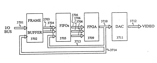
Another irnplementation adds direct wnte-back to the frame buffer. ReferIing
, .~
to Figure 37, I/O bus 3701 writes to frame buffer 3702, which in ~rn is the source
of a ~rst video stream 3703 connected to a first input ~IPO 3705 which is connectecl
in turn through a first bus 3706 as an input to FPGA 3709. A second source stream
~25 3704 may originate from frame buffer 370~ or may originate from a second,
:~ independent source (not shown). Source stream 3704 is connected through a second
input FIFO 3705 and a second bus 3706 as a second input to PPGA 3709. The
output of FPG~ 3709 is connected over bus 3710 to DAC 3711, which i;Sl ~rn feedsideo line 3712. FPGA 3709 output is also connec~ed to bus 3713 to provide arl ~,
~30 input for a ~hird FIFO 3705 which acts like the history F~O 3510 in Figure 35.
FIFO 3705 is connected through a third bus 3706 to a third input of PPGA 3709.
'~ ''! '
,~,'
. W094/l06~4 ~33~ 21~8~1~ PCr/US93/10677
The output of F~GA 3709 is ialso routed through bus 3714 to provide a second input
to frarne buffer 3702. This allows performing bit blit operations combined with
~PGA functions to modify the source of frame buffer 3702.
;....... ~ .~
The ~mplementation just described can be augmented by providing local
.' memory, such as static RAM, for the FPGA. Refe~ng to Figure 38, I/0 bus 3801
i~l provides ian input for frame buffer 3802. Source streams 3803 and 3804, ~nput iand
i~ history ~l~`Os 3805, buses 3806, 3810, 3813 and 3814, DAC 3811 iand vldeo line
~1 3812 are equivalent to the corresponding components in the system of Figure 37.
. ,~
~, 10 The system of 38 adds fast cache memory, such as SRAM 3816, connected to FP&A
~ 3809. SRAM 3816 can store useful ~fonnation so that the overall system can now
';, perform pattern f;ll, character fill or keyed coefficient operations. In addihon, the
system can include channel look-up tables.
~l 15 The second general class of video processing devices discussed above provides
off-screen video processing.
. ~
In a typical video processing device, there is only one frasne buf~er. That
~e buffer becomes a very precious resource because the output sec~on must read
from that frame buffer and the input section must write to it. Many opera~ions
typically are performed by rnodifying the frame buffer. These include masking, bit
blit~ing, zooming, interpola~ing, iiltering, and many other operations.
By providing mul~ple frame buffe}s, one of ~e buffers can be selected as the
current ou~put ~me buffer to provide a video feed while information in the
~ r~maining buffers is processed for subsequent output. Cycling through mul~ple
j~ frame buffers can provide a very high frarne rate, whieh translates to more ~me to
process each iiame while it IS off line.
One preferred embodiment of such a system is a "ping-pong" frarne buffer
system which includes mul~ple frame buffers, mul~ple processing units, and a large
crossbar swi~ch. Such a system can move 20 megabytes of video info~ on in lOO
.
WO 94/10624 ~ ~ 34 ~ PCr/USs3/l0677
2~4~814
nanoseconds, then another 20 megabytes in the next lO0 nanoseconds, by switching
among several frame buffers.
i~ ,
;1 Referring to Figure 39, IIO bus 3901 provides input to VGA section 3902, the
,,,3 5 output of which provides input to a conven~onal Yideo stream 3903 (for ulhmate
display - not shown) and a second, bidirectional connechon to crossbar switch 3905.
VGA section 3902 can be a conven~onal video display board, but the frame buf~er
has been moved and now is to be connected through crossbar switch 3905. Crossbarsw~tch 3~05 is connected to multiple DRAM frame buffers 3906, any one of which
10 can act as a frame buffer for the video system. Crossbar switch 3905 can cross
cormect a large number of leads, such as a group of 32 bidirechonal ~ines from VGA
section 3902 and 32 lines from a first ~rame buffer DRAM 3906, and simultaneously
and independently connect a group of lines from a DSPmod, descr~bed above, to a
~second frame buffer DRAM 3906, and so forth Currently available crossbar
switches can independently connect ten 50-pin buses (500 pins) with less than a 10
nanosecond delay.
In Figure 39, second l/O bus 3901A ~nterfaces with each of four FPGAs 3911,
each of which are connected to four DSPs 3912 and to crossbar switch 3905 and, i~
selected by crossbar switch 3911, to one of frame buffer D~AMs 3906. One
;~ preferred implementation uses a DSPmod, as described elsewhere in thisspecification, for each group of one FPGA 3911 and four DSPs 3912. More
complex switching is possible, if desired, such as connection of one DSPmod to more
than one DRAM 3906. For example, one DSPmod might process the first quarter of
the frame in each f~ne buffer l:)RAM 3906 while each of three other DSPmods
~` processes corresponding portions of the remaining frarne b~ffer DRAMs 3906.
~;l Pr~mary I10 bus 3901 may be connected to ~e H-bus of the overall system
~, desclibed throughout this spccifica~on. I/O bus 3901A may be an M-bus, connected
30 through a bridge module (not shown) to t~e H-l~us, to provide bidirec~onal
commutlica~on with one or more DSPmods.
~ t
,`,
,;; .
; .
WO 94/106~4 2 ~ 1 8 S l ~ PC~/US93/10677 ;
` !''i`: ';'
`, Another prefer~ed embod~ment is optimized for copying frames. Referring to
t Figure 40, I/O bus 4001 provides input to VGA sechon 4002, the ou~put of which
~, provides input to a conventional video stream 4003 and a second bus connection to
frame buffer DRAM 4005 and over DRAM bus 4004 to each of multiple (two
i 5 shown) FPG~s 4Q14. l~rame buffer DRAM 4005 is the principle, if not sole, frame
1~ buffer for the video output section. A second IIO bus 4001A interfaces with each of
two PPGAs 4011, each of which are connected in ~rn to four DSPs 4012, a memory
i~ device 4013 such as a 4 MB SRAM, and to FPGA 4014. In a pre~erred
,') embodiment, this eonfigura~on is achieved using two DSP/PLDmo~s.
~ This system works well w~th DR~-based frame buffers. Using the system,
~he current frarne easi~y can be copied into module memory 4013 or the contents of
module memory 4013 can be transferred to frame buffer DRAM 4005 for display
through the standard video s~eam 4003. A frame copied into module memory 4013
can be processed, then rewritten to frame buffer 4005 for display. In general, if a
~e is to be processed before displaying, it will be directed to the memo~r modules
ISrs~, and only after processing to DRAM 4005. Dua~ ~rame buffers can enable
simple, real time interleaving.
, ,
, 20 Still another preferred embodiment is a slight varLa~on on the system of Figure
40, using a frarne buffer D~AM as the principle video f~me buffer, not an alternate
~rame buffer. Referring to Figure 41,1/O buses 4101 and 4101A, FPGAs 4111,
DSPs 4112, and memory devices 4013 are connected and funchon essentially as
described for corresponding components in Figure 40. VGA 410~ is written by I/O
~S bus 4101 but has a single output, connected to the input of frarne buffer DRAM 4105
and to a bidirectional bus to each of "zero" delay ~"0 ns"~ buffers 4114 (preferably
~i~ less than S ns devices). F~e bu~fer DRAM 4105 can be read out to provide output ~ -
through video stream 4103. Alterna~vely, the module memory 4113 can be accessed ~`
directly ~rough æro delay buffers 4114 to provide video output. This allows
~30 random access for more flexibl~ display or to allow bit blit~ng within frame bu~fer
1.l D~ 4105.
~i
`~1
.
. ~ . .
.1
WO94/10624 214~ 36- PCI/US93/10677
':~ . ':. i .
A simple preferred embodiment ~ncludes only one FPGA and one DSP in the
video processing section. ReferriIIg to Figure 42, I/O bus 4201 provides input to ,'
` VG~ section 4202, the ou~put of which provides input to a conventional video stream
4203 and a second bus connechon to fra?m?e buffer DRAM 4205 and over DRAM bus
4204 to ~GA 4221. DSP 4220 is connected to FPGA 4221. FPGA 4221 cian be
,~ configure~ to emulate a ~RAM fiame buffer and may, for example, hold some
,~ number of rows of pixels for subsequent output. DSP 4220 can set up drawing
"`, pararneters or can process information in ~PGA 4221. VGA 4202 can eopy
.~ ~ information from FPGA 4221 to frame buffer D~AM 4205 using a bit blit operahon.
VGA~ 4202 also can copy infonnation frame buffer DRAM 4205 to DSP 4220 using a
bit blit operation. A significant advantage of this system is its, low parts count and
low cost to build.
~ ?`,'
?~ ` Another preferred embod~rnent uses the frarne copy system of Figure 40 but
with additionial modules for increased processing power and using video RAM
~, (VRA~ instead of a DRAM fr~ne buffer. Referling to Figure 43, providing four
DSPmods, each with 4 megabytes of on-board memory, allows for more processing
operations on information stored in the frame bu~fer DRAM. The system is designed
to conforrn to an S3 VRAM type interface and the PPGAs can serve as a data source
during bit blit operations.
Using ~ instead of a DRAM frame buffer provides some advantages. A
DRAM frcune buffer cannot be accessed simultaneously for writes and read-out to the
video output system. A ~M, however, has both a serial output port for video
ou~put plus a random access port, useable for reading or wnting. No~ly, the
YRAM is written by the VGA section through the random access port, but such
writes are not constant, in fact leaving that port accessible most of the ~e. The
configuration shown allows the DSPmods to access the VRAM through its random
i~}; J access port when it is not otherwise in use.
:,
.
~`l 30
~(t The principles of the Vmods discussed above can be utilized to good advan~age
in an improved embodiment, referred to as an rtDSPMod, for rea~ ~ne video
'. .
; ,:
~,
, .
: .
WO94/106~4 - 37- X~ PCr/US93/10677
~! processing. Re~erring to Figure 44, H-bus ~9 and M-bus 6Q connect to a first PLD
3 4411, preferably a Xilin~ XC 4004. PLD 4411 is connected through address bus4430 and also through data bus 4420 to one or more ~referably four) DSPs 441~ and
`i RAM 4413. Bidirectional address bus 4430 is connected to "zero" delay buffer~4432
S which is connected in ~rn to address bus 4431. In a similar way, bidirectional data ~:
bus 4420 is connected to "zero" delay buffer 44~ which is connected in turn to data
~:1 bus 4421. Address bus 4431 and data bus 4421 are connected to each of RAM 4414
;~ and PLD 4ll5, preferably a Xi~ XC 4005. PLD 4415 is connecte~l in tum to each
of N-bus 4440 and O-bus 4441. The N- and O-buses are typically connected to a
10 video stream and PLD 441i is typically configured to modify a video signal as it
~i~, enters on one bus and exits on the other.
~;
This module provides a number of useful benefits. In a ~ypical
implementation, PLD 4411 is configured with logic to interface with the system H-
bus and M-bus as well as other resources in the rtDSPMod. PLD 4411 can receive
configuration inforrnation and, utilizing the connected DSP and RAM resources,
calculate and store appropnate data. In a typical application, these resources are used
to prepare configuration and data information for use by PLD 44lS and its associated
, memory, RAM 4414. Buffers 4422 and 4432 can be enabled so all resources in the
,~ 20 module are in cornrnunication, allowing resources 4411, 4412 and 4413 to load
configuration and data information into 4414 and 4415. Depending on the specificapplica~on, the configuration of PLD 4415 can often be loaded and left for some
~ ~ne. Buffers 4422 and 4432 can be disabled to disconnect the resources on the left
``.'!. side of the figure so as to not ~nterfere with video stream processing. If desired, the
rcsources on the lèft side can then calculate a subsequent configuration or perform
other tasks. This dis~ibu~on of ~esources allows PLD 4411 to be op~nized for bus-
interface and communica~on logic and frees up essen~lly all of PLD 4415 for video
processing logic.
`1 s
,.. ~ ~.
. . .
~30 An alternative comSgura~ion uses a single large PLD Ln place of the two PLDs
shown here. However, commercial devices available today have a limited pin count
.
. ~,, ~,
WO94/106~4 2 d~88 1~ - 38- PCI/US93/10677
and lirnited logic rescurces and in general cannot provide enough logic resources to
load complex video processing logic in addition to the necessary mterface logic., ~ ~
`i The video stream processLng described above benefits from designing logic
S flow so that a series of calculating devices can sequen~ally modify a group of pKels
in a pipeline f~shion. Many of the modules described above can be connected in
. . ..
series to perform a calculation on a group of data, then pass the data along for further
i manipulation in the next module. This arrangement is often called "systolic".
¦lo The rd:)SPMod illustrated in Figure 44 is particularly useful in a systolic
processor. Referring to Figure 45, in one preferred implementation, frame bu~fer4502 and video line interface (VL I~ 4521 are connected ~ogether and to the system
video signal through video line (VL) bus 4512. Frarne buffer 45~2 is also connected
through M buses 60, N-buses 4540 and O-buses 4541 to each of eight rtDSPMods
~15 4544. VL I/F is also connected to each component in the figure through M-bus 60.
;~ ~s described above, the M~bus preferably is used for configuration¦ information and communication between mcdules while the N- and O-buses are used
for video processing. The N- and O-buses are connected in parallel between each
~20 top/bottom (as illustrated) pair 4544A, .. 4544D of rtDSPMods, with a serial
cormec~on from one pair of mods to the next pair to the Iight, with a final return ~o
~1 the ~e buffer. This con~gura~on ~llows four stages of processing.
`,;''1 ,
VI. I/F 4521 manages comrnunication between a host (no~ shown~ over an H-
;`2~ bus (not shown~ and each of the o~er components in the figure using connec~ons and
methods described generally throughou~ this specifica~on. Since the buses of this
invention are programmable, selected lines of M-bus 60 can be par~oned and
connected in each device to act as an H-bus. VL I/F 4521 also con~ols the motion of i;
video data between ~rame buff~r 4502 and the rOSP~ods. For example7 VL I/F 'i
` 30 4!~;21 might control a bit blit~ng operation on video ~rarnes.
... ~ -.
. .
.c:" ~
WO94/106~4 1~8l~ PCI/U593/10677
Uise of a systolic array or processor is known in the art. For example, mod
pair 4~44A might be used to select tex~re coordinates for each pixel in a video
stream. Mod pair 4544B might then look up and interpolate the texture coordinates.
Mod pair 4544C n~ight then scale the video for display and mod pair 4544D might
S remap the color, for example to adjust linea~ity or color purity. A systolic processor
is not good for fine grained logic implementatiorls, but is particularly useful for
coarse grained logic and par~cularly well suited for processing large blocks of data.
The illustrated implementa~on allows for real timie video proceissing, which in
general is not available with any other econorr~ical system. Full ~rame rate processing
simply cannot be handled using software-only sys$ems and complex multi-node
processors are not only difficult to program bu$ also, for the most part, do notprovide the processing power of the present system. PI Ds such as gate arrays
provide sufficient processing power but before this time, no one has been able to
connect and and control enough gate arrays to provide a use~ul real time video
processor.
Still another preferred implementaaon is illustrated in Figure 46. Refening to
~ Figure 46, eight rtDSPMods are shown, including PLDs 4611, 461S, DSPs 4612 and
`~:`,''!1, 20 RAM 4613, 4614. Zero nanosecond buffers 4622, 4632 are illustrated as a single
i block in each module. H-bus 59 and M-bus 60 is connected to each module and N-
bus 4640 and O-bus 4641 are routed between modules substan~ally as illus~ated inFigure 45. Frame buffer 4602 and YL I/F 4621 are connected substan~ally as
illustrated in Figure 45. In addition, Figure 46 shows optional configurahon R~
~i 25 4625 which can be connected to VL ItF 4621 to load an ini~al or start-up
~' configu~ation. PLD 4626 can be connected to a system bus such as an ISA bus for
communication with external devices~ Cross-bar switch 4605 can be connected
through S-bus 67 to cach module (preferably through PLD 4611) for selective
signalling between specific modules.
;~,~ ,, j
wo 94/1~624 2 1 ~ ~ 8 1 ~ PCI'/US93/10677
Cor~fi~urable Buses
,¦ The configurable bus of this invention is a powerfi~l tool, providing flexible
'~1 comrnunication within an adap~ve architecture device. Each line of a bus connecting
at least two PLDs can be assigned a different function at different time points,5 changing infrequently or frequently, even several to several hundred times per`1 second. This allows highly flexible communication between devices. Hardwired
lines between a soclcet and a PLD be configured to accornmodate di~ferent signals for
the same pin position on different parts. In addition, future devices will include
programmable pin assignments for memory and other devices.
' 10
In one configuration, a bus can be configured to consist mos~ly of data lines,
ij~ to transfer large amounts of data. In another configurahon, each of several devices
may be assigned a unique bus line, providing asynchronous communica~on between
devices to, for example, signal inte~upts or bus requests. In general, it is preferable
to include a clock line and a reset line between each device. This may be part of a
configurable bus or, preferably, it rnay be a designated separate line to each device.
I.
A bus protocol can be similarly modified according to the prograrnming of
each PLD device. These protocols may need to interface with existing bus protocols
for communication with external devices or may be op~ni~ed for internal
comrnunication. An initial bus protocol and bus configura~on are generally loaded
'l .
~¦ along with an application and may be reloaded or modified under control of an
application.
A few representative bus architec~res and protocols are discussed here but the
possible varieties are almost limitless. Referring to Figure 16, each DPU 80 has one
or more buses of many lines each. A typical DPU of this inven~on is connected tolj three such buses, an M-bus, an N-bus and an internal L-bus ~see Figures ~-7 and
`~! related discussion). Each bus pre~erably has 20 lines, each connected ~o a pin on
DPU ~0. These lines for each bus can be allocated independent~y in a var~ety of
configurations.
.; . .
.
,.. !
.~ WO 94/10624 - 41 ~ 2 1 ~ ~ 8 1 4 Pcr/usg3/~0677 1`,"
' '!~ ,.
1:"; : " '
Figure 16A illustrates one irnplementation of a standard 16-bit bus. Sixteen
(16) lines 104 are allocated as data ~ines. Addi~ional lines are ~ssigned as single-
function lines for address signal AS 1~, read signal RS 106, write sign~l WS 107and an OK or acknowledge signal 108. A PLD within DSP 80 configures these~lines
S to connect within DSP 80 to corresponding functions address, read enable, and write
enable, and aclcnowledge, respectively. The corresponding ~ning diagrarn of Figure
16B shows that at to when AS 105 and RS 106 and OK 108 are each high, the
. remaining bus conten~s are ignored. After DPU 80 arbitrates for bus control, AS 105
goes low at tl signallirlg that an address will follow on data-lines 104. As high
~10 address (ahi) bits are clocked in at t2, AS 105 stays low, signalling that low address
~alo) bits will follow. RS 106 goes low at t3, signalling that a data block follows on
data lines 104. One clock later, RS 106 goes ~gh and OK 108 goes low, signallingthat data lines 104 now carry one block or a specified number of sequential blocks of
valid data. One or rnore clock hcks later (shown at tS but possibly many ticks later)
15 OK 108 goes high to achlowledge successful reading and subsequent sîgnals on data
lines 10~ are ignored. A data block can be chosen to be a specific or a variable size.
The read cycle may con~nue for several clocks but a single clock read is illustrated.
At the completion of the read cycle(s), RS goes high. If the data was success~ully
read, DPU 80 sends an OK signal at time tX+l.
An alternative bus architecture is a dual 8-bit bus. Referring to Figure 16C, 8
~ines 104A are allocated to data for bus 0 and 8 lines 104B arè allocated to da~a for
bus 1. Single lines are provided for cycIe0 ~ine 109A and OKo 108A for bus 0 andcyclel line 109B and OKl 108B for bus 1. The data lines are cycled between
address/con~ol signals and data and the cycle line specifies the current state. This ~1
could be modified to have several packets of address infonna~.on, con~ol infonnation
or data car~ied on ~e da.ta lines. The corresponding timing diagram of Figure 16D
for bus 0 shows that af~er cycleQ 109A goes low at ~me to~ data.0 Iines 104A carry
address signal AS, write sign~l WS, read signal RS, and may carry other signals as 1 -
~30 well. After cyele0 109A goes high at tl, dataO lines 104A carry data signals, which is
.. j,ll i
. . i: ..
~ .
~1 `
~! WO 94/10624 2 1 4 8 8 1 'I -- 42 -- PCI/U593/10677
` conf;rmed by OKo 10~A going low. This process is repeated in one clock unit at
time t2 and t~rne t3 and SQ on.
;~ Yet another alternative bus configura~on is a set of single line buses.
S Referring to Figure 16E, sixteen buses, each comprising a single signal ~ine 104, can
`~ carry 15 signals to 16 sets of locations or other buses. Sync ~ires 110 are used to
~n assure proper ~im~ng. Providing separate sync lines 110 allows signals to travel
¦ varying distances and to arrive at I)PU 80 at slightly different times. The ~ing
diagram in Figure 16F shows how a representative signal line, SIGN0 104 carries a
10 packet of signal address bits beginning with high order bit an through low order bit aO
; between tLme to and t2 (or longer, depending on the protocol) followed by a data
t~,~ packet starting with high order bit dn through low order bit do beginning at time t2.
, .,
This may be followed by more data packets or another address packet immediately or
after some delay. Serial transmission of information is well understood in the art and
,` ~15 one can readily design a protocol to work with the buses illustrated in this figure.
',.: ;!
!
~i A bus may be partially hardwired, thus not configurable. This is particularly
applicable for connections to outside, non-configurable devices such as an ISA bus or
` :¦ SCSI bus or a modem or pnnter. :E~eferring to Figure 16G, DPU 80 is connected to
`;`~20 a first bus VARo lllA of three lines, to a second bus VAR~ lllB of eight ~ines, and
to a third bus VAR, 11lC of five lines. As in the implementation shown in Figure,~1 16E, four SYNC lines 110 are provided to coordinate data transfer. A bus may be
; ~ partially hard wired and par~ally configurable. Refernng to Figure 16H, serial line
S'~i 67 and VAR0 111 are hard wired to provide ~our lines and six lines of
~;j25 colrununication, respectively, while eight data lines 104, clock 109, and OK 108 are
~: ,
reconfigurable.
;.i,
;,............................................................................ . ..
Finally, a simple stand-alone device built around the PLD of ~e invention can
',` i make use of reconfigurable buses. l~efening to Figure 16I, program con~ol portion
32 of DPU 80 is connected through a f;xed bus to EPROM 12, containing a boot-up
configuration and data. An LED readout 112 and keyboard 113 (not shown~ are each
WO94/10624 3~ 21~8~ P~/U~93/10677
~ii conneet~d through a fixed bus to DPU 80. Analog to digital converter (ADC) 114 is
connected to DPU 80 through 9-line, configurable bus 116 and sync 110A and digital
to analog converter (ADC~ 115 is connected to DPU 80 through single-line,
configurable bus 117 and sync 110B.
~, 5
Another protocol, not illustrated, allows for absolute time to be known by
essentially all devices in a system. The individual clock counters are reset, for
~;i example when the system is powered up, and some or all commands are expected to
occur at a specified tirne~ Devices then simply read or write a bus at the designated
10 time. This obviously has the potential for great complexity but also may offer
~.~
,~ significant speed benefits, eliminat~ng the need for bus arbitration, address packets,
j control packets and so forth.
:''
The bus protocol can be allocated according to need under the control of a
lS cornpiled host prograrn, possibly with modification by specific application C code
~nstructions. In general, all buses share a Clock-Line and a Reset-Line. Bus
~,~
configuration and protocol data is preferably downloaded when the application is first
loaded and may be reloaded under control of the applicaaon. Reconfigurahon data
can be loaded in less than about 10 rnilliseconds. In order to address each DPU
20 directly, each DPU can be assigned an address based on a physical slot or
xelationship within the system. DPUs can be provided with ~egisters and intemal
memol~ holding an offset address. DPUs may store and forward packets of data as
`'`,t needed.
! ~5 The configurable bus o~rs significant benefits in terms of flexi~ility but it
, ` comes at a cost. The configurability allows imp~ementation` of large combinato~ial
logic funetions, useful for rapidly solving complex branch or case tests, such as can
curren~y be done only by designing a specific circuit, typically as an ASIC.
,~ Execu~on of complex logic can be performed considerably faster than on a general
30 purpose computer, but not as fas~ as on a true ASIC. However, the configurabi1ity
means that the new device can fi~nction as one ASIC for a periodi of time, t~en be
quicldy reconfigured to func~on as a different ASIC. New generahons of PLDs will
~ ~ WO 94/l0624 2 14 ~ 8 14 PCI/US93/10677
have faster circuits ànd will reduce this speed difference considerably, although it is
unlikely that a fully reconfigurable circuit will be 100% as fast as a custom designed
`~ c~rcuit fixed in silicon.
.,,,
,
~ 5 U~ng the rnod?~es
';!~ ` The modules and EPU described above can be configured to run one or more
~, programs. A complex program may require many such signals, and can consume a
~ large porhon of valu~ble, available circuit area and resources. A reconfigurable
;` device could allocate resources for signals only as needed or when there is a high
',`~' 10 probability that the signal will be needed, drama~cally reducing the resources that
must be committed to a device.
, ' ,!
` i'i
`` Certa~n operations run better ~n specific hardware. For a conven~ional CPU
, ....
with cache memory, registers and ALUs, these operations include data mar~ipulation
;! ~ 15 such as arithmetic func~ons and compares, branch and jump instructions, loops, and
other data intensive filnctions. Other opera~ions are more easily h~ndled in special
hardware, such as ADC, DAC, DSP, video frame buffers, image scanning and
~1 printing devices, device interfaces such as automobile engine sensors and controllers,
and other special purpose devices.
~20
Stre~ompllinR Al~orithmic Source Code
Conventional programrn~g for a general purpose computer begins with a
prograsn written in any onei of several suitable computer languages, which is then
compiled for operation on a certain mach~ne or class of machines. Programming inJ 25 assemb~ language gives the programmer detailed control over how a machine
fimc~ons but such pr~,~g can be very tedio,us. Most programrners prefer to
w~te in a rehtively high level language.
,.
The present device provides a greatly enhanced li~,rary of fimctions available
30 ~ to a computer program. Essen~ally, a convenaonal source code program can beconverted in whole or in part into a series of specialized circuit configura~ions which
will use the sa ne inputs or input informa~on to produce the same result as the
~.
WO 94/10624 1 ~ ~ 81 ~ PCI`/US93/10677 ~;
conventional progran~ running on a conventional computer but the result can be
provided much faster Ln many cases. A wide variety of functions can be implemented
in hardware but can be accessed by a subroutine call from a main prograrn.
S Where a cvnventional programmer might code to initialize two variables, then
~i add them, a general puIpose CPU must allocate memory space for the variables, at
least isl a registerJ then load an adder with the numbers and add the values, then send
~`, the result to memory or perhaps to an output device. Using a DPU, a PLD can be
configured to add whatever is on two inputs, then direct the result to an output. For
~10 this simple operation, a DPU may not provide a significant irnprovement in ease of
calculation in comparison to a conventional computer.
, .,
,!1 The benefit of a DPU can be considerably greater when the desired opera~on
is more complex. For example, pLxel information may be provided in one or more
bit plane forrnats and n ay need to be converted to another format. For example, the
input may be a raster image in a single plane, 8 bits deep. For certain applications,
~ this may need to be converted to 8 raster image planes, each 1 bit deep. The first bit
:3'`. of each pixel word needs to be mapped to a first single-bit plane pixel rn~p, the
second bit to the second single-bit plane pixel map, and so on, to give eight single-bit
20 plane pixel maps w~ch correspond to the orig~nal ~-bit plane. It is relatively simple
to configure hardware to split and redirect a bitstTearn according to a certain rule
s~ucture. This sarne method can be modified to combine eight single-bit planes into
a single 8-bit plane, to create four two-bit planes, to create two four-bit pl~nes~ to
maslc on0 bit plane against a second bit plane, and so on.
~25
A par~cular applica~on may frequent~y call one of several specilSc conversions
(expected to be called f~quently by ~e program or ~e user) and call other specific
conversions less frequently. A compiler can calculate logic configura~ons to execute
each of the comrnon conversions and load the configurations simultaneously so ~at
~0 any is available simply by selec~ng ~e appropnate inputs. If there is limited PI,D
space available, configurations can be calculated and stored, ready to be loaded on an
as-needed basis. If there is sufficient PLD space available, even the less~ uently
.~
.,
~i W{)94/10~4 ` ` PCI/US93/10677
called conversions can be resident in a PLD for immediate access when the need
arises. By confi~uling a I)PU with equivalent informahon, each of most or all likely
; i, inputs can be processed within a ~ew clock cycles by providing a configuration for
^` ~ each lil~ely input value and then simply activahng the appropriate poraon of the
~^i 5 circuit.
: ~ .
;' The implementation begins by analyzing an algoritl~nic language program and
converting as much of that program as possible to run on available hardware
` ~ ~ resources. Many hardware languages are available and known, to varying degrees,
~, 10 by persons skilled in the art~ These languages include ABC~/l, ACL, Act I, Actor,
ADA, ALGOL, Amber, Andorra-I, APL, AWK, BASIC, BCPE, BLISS, C, C++,
C~, COBOL, CollcurrentSmallTaL~c, EULER, Extended FP, FORTH, FORTRAN,
GHC, Id, IFl, JADE, LEX, Linda, LISP, LSN, M~randa, MODULA-2, OCCAM,
~;~ Omega, Orient84/K, PARLOG, PASCAL, pC, PL/C, PL/I, POOL-T, Postscript,
~15 PROLOG, RATFOR, RPG, SAIL, Scheme, SETL, SIMPL, SIMULA, SISAL,
SmalltaL~;, SmalltaUc-80, SNOBOL, SQL, TEX, WATFIV and YACC.
~;J In a preferred embodiment, the C language is used ~or source. This provides
t~ several advantages. First, many programmers use C now and are familiar with the
20 language. Second, there are already a large number of programs already available
which are written in C. The C language allows simple ~nplementa~on of high levelfunctions such as s~ucn~res yet also a~lQWS detailed man~pulation of bits or str~ngs,
down to machine code level. The C language, especially with some simple
1 extensions, is also well suited to object-onented programn~ing, which also works well
25 ~with the present invention. Third, the C language is now so widely used tha~ many
translators are available to translate one language to C. Such translators are available
for FOl~T~AN and COBOL, both popular languages, and translators exist for other
languages as well. For convel~ience, the C program will be used as an example, but
one skilled in the art will recogni~e how to apply the teachings of this invention to ~
30 use oth~r algori~c languages.
I,: b, . "~ . ..
,`.,,, l
W094~10624 ~ 47 ~ 214~814 Pcr/uss3/~o677
:` j '. ` 1'` '
The method ir~cludes ~our sequential phases of translation, a tokenizing phase,
a logical mapping phase, a logic optimization phase, and a device specific mapping
~, phase. Current compilers tokenize source code instruchons and map the tokenized
instructions to an assembly language f;le. For instruchons written in hardware ~description languages, there are logic optimization routines, but there are no current
methods to convert algorithmic source code into a hardware e~uivalent. Source code
,~ instructions suitable for implementation in a PLD include a C operator such as
mathematical operators (+, -, *, /~, logical operators (~;, &&, I l). and others, a C
expression, a thread control instruction, an I/O control instruction, and a h~rdware
implementation instrucaon.
A programrner begins by preparing a program for a problem of interest. The
program is typically prepared from C language ins~uc~ions. The basic prograrn
! functionality can be analyzed and debugged by traditional methods, for example using
a Microsoft C compiler to run the program on an MS-DOS based platform. This
sarne C code, possibly with sorne n~inor modifications, can be recompiled to run on a
configulab1e architecb~re sys~em.
The sl~earn splitter separates C instructions in program source code ~n order tobest implement each mstruction, allocating each ~nstruchon to specific, available
~? hardware resources, e.g. in a DPU, or perhaps aUo~atmg some unshuctions to run on
a host or general purpose computer. Referring to Flgure 17, s~eam spliKer 202
splits C program source c~de 201 mto portions: host C source code 203 that is best
suit~d to lun OQ a host CPU; PLD C source code 204 that is best suited to ~un on a
~25 PLD of this inven~on; and DSP C source code Z05 that is best suited to run on a
DSP. Compilation re~uires lib~ rou~nes are available to provide ne~ed
resources, especially pre-calculated implementations for certaiIa C ~struc~ons and
par~oners and schedulers to m~ge intennodule control flow. Par~oner and
scheduling resources 203B are added, as needed, ~rom par~oner and scheduler
~30 L~rary 202A to host C sou~ce code 203A to coordinate calls to other por~ons 204,
20~ of the C c~de which will be implemented in hardware. Co~nunica~ons
` i resources 203C, 204B and 20~B are added to C source code porhons 203, 204, and
. . .:
;,,
wo 94/106~4 2 ~ 4 ~ 814 Pcr/uss3/loa7 ~ ~
205, respectively, from comrnunica~ons LIBrary 202B, as needed, to provide needed
, library resources to allow the system resources to interact once compiled and
implemented in the system. Host C compiler 206A combines and compiles host C
;' source code 203A, partitioner and scheduler resources 2û3B and communicahons
Z S resources 203C into executable binary file 207 and corresponding po~ons 207A,
~: 207B and 207C. PLn C compiler 2n6B combines and compiles PLD C source code
~; 204A and cornrnunications resources 204B into executable binary PLD configuration
~le 208 and cor~esponding portions ~08A and 208B, respectively and DSP C
compiler 206C combines and compiles DSP C source code 205A and communications
resources 205B into executable DSP code 209 and corresponding por~ons 209~ and
, 209B, respectively.
~Z
PLD code must ul~rnately operate on PLDs within the system and preferably
includes configuration data for each PLD and for each configurahon required to
15 operate the system. PLD C source code must be translated or compiled to
configuration data 208 useable on a PLD. One or more configurations must be
prepared for essentially each PLD needed to operate a selected program, although not
all programs will require all of the PLDs available in a given system. In gene~l,
configuration data must be provided for repmod, bridgemod and DPU PLDs,
~20 including ~GAmod PLDs. For Xilinx parts, the C source code must be translated to
a .Bl'r file, possibly through an intermediate compilation to .XNF fo~nat. DSP code
must ul~mately operate on DSPs within the system and preferably includes
il configura~on data for each DSP and for each configuration required to operate the
system. DSP C source code must be translated or compiled to executable machine
25 code 209 for a DSP. Manufacturers of DSPs typically provide a language and
compiler useful in generating DSP~ machine code. DSP C source code 205A may be
translated into an intermediate form before compiLation into final machine code 209. !-
. .
The result of s~eam spli~ng is illus~ated in Figure l9. An original C source ~
;~ 30 code program 201 may contain a senes of three sequential function calls, funchon 0 `~
I 240 followed by function 1 24I and funchon 2 24~. When executed on a general
. ` .
:
.
.
,!,
W094/10624 - 4~ 4~ 1 Pc~/US93/10677
purpose computer, each function is executed one at a ~me in order. Each functionmay be quite simple, such as add two numbers, or may be ~uite complicated, such as
convert a single 8-bit plane raster image to four two-bit plane raster images and mask
OR) the first two-bit plane image against the sum of the second and fourth two-bit
~ S plane images. If function 1 24l can be implemented more efficien~ly on hardware,
`~ the stream splitter can analyze, convert and compile that function to run as funcl:ion
241A on a hardware resource such as a DPU and simply insert a MOVE DATA
command 243 into the execution stream of the host prograrn, coupled with an
EXECUTE I)ATA command 244 on the DPU. If function l does not return any
~10 value and function 2 does not depend on the result of function l, or if funchon 2 does
not need the result of function l and function 2 will take longer to execute than will
function l, then program control can pass imrnediately to function 2 242.
Alternatively, if function l does re~rn a value needed by function 2 then function 2
can wait for execution to complete. During execution, parameters needed by funchon
;';~ 15 1 are passed to the DPU(s) holding filnc~on 1 via DPU bus connections. Functions,
;~ whether on the host or on a I)PU, may call one or more other funchons, each of
which may be on the host or the same or another DPU.
The slream ~plitter is especially useful for automatirg data ilow for:
parameters passed and returned; global variables; and global arrays. Usefill libraIies ~`
in partitioner and scheduler LIBrary 20~A and co~unications LIBrary 202B
include: scheduling heurishcs, libranes and templates; data conversion utilities;
DMA; and FIFOs.
;ii~
A par~cular func~on is preferably implemented wi~hin a single PLD but larger
algoritluns can be par~tioned between multiple PLDs and even between multiple
DPUs. An arbi~arily large algorithm can be implemented by providing enough DPU
modules.
'~
``'`l
:i;30 Referring to Figure 20, the conversion of original source code to parhtioned
j .~
functions can be better understoo~. Standard C source c~e 251 can be modified by
a progra~T~ner to include compiler ins~uctions to partition certain funchons into select
., ~ .
,
;`'.
;
, . .
WO 94/10624 2 1 4 ~ 8 1 1 PCI'/US93/10677
hardware resources. Mc)dified source code 252 includes ~DSP" and ~END-DSP"
comrnands around "funl {..} " to instruct the compiler to implement this function as a
DSP operation. A precompiler partitions code 252A into host code 2~2B (equi~alent
to 203A in Figure 17) with a "MC3V-DATA; ~"funl",DSP)" call inserted in place ofthe original function code. That ii~nction code is partitioned into DSP code 253 -
(equivalent to 205A in Figure 17). The source code is supplemented by host source
library routines 254 and DSP library routines 25~. Additional code (not shown) is
required to establish comrnunication between the host and the DSP.
,,
The method of compiling is illustrated in Figure 21. Referring to Figure 21,
given a specific configuration of DPU hardware 261, compiler 260 applies an input
Slter, then collects data on the environment, including the DPU hardware
~, configuration and available resources, capacihes and connectivity. The scheduler-
partitioner contains information on function and data dependencies, commiunication
~15 analysis, plus node alloca~ion, partition, schedule and debug strategies and schedule
;, maker constraints. The code generator and library provide additional resources for
3 the maker to convert C source code using a third party C compiler plus an enhanced
C syntax analyzer and C to PLD compiler to first tokeni~e the input source code,then prepare a logic map including variable alloca~on, C operators, expressions,~20 thread control, data motion (between components and fuIIchons) and hardware
'i~ support. The logic map is then evaluated for possible logic reduction and f;nally
mapped to the available devices, as needed.
. The present system allows a linear prograun to be pipeilined in some cases.
25 Figure 22 illustrates a traditional single CPU, general pu~pose computer with a main
prograrn 270 which calls func~on 1 271, waits for execution, then calls fùnc~ion 2
i~ 2n, which in ~m calls funchon 3 273, which completes execu~on, function 2
completes and passes control back to main program 270. By way of comparison,
Figure 23 illusbates the same program implemented in a distributed system.
;l30 Assllming func~on 1 is amenable to partitioning ~e.g. remapping a bit plane - half of
the plane can be assigned to each of two processors), the program can work that
much faster. Mairl program 270A on the host system again calls funcaon 1 271A but
`
,
WO 94/10624 - 51 _ 2~ pcr/us93/10677
271A calls servers 270B and 270C, each of which call corresponding function 1
~i portions 271B and 271C. When execuhon is complete, the servers notify host
function 1 271A, which notifies main program 270A and 270A calls function 2 272A.
l~epending on the interrelation of funchon 1 and function 2, function 2 may be ~S caUable before function 1 is completed. Function 2 272A ca~ls server 270A which
caUs function 2 272B, which in ~urn calls funchon 3 ~73B. When 273B and 272B
have both completed, control is passed back all the way to host mar,l program 270A.
,
The process of converting C source code to a device configuration is illus~a~ed
in Figure 24. Briefly, source code 281 is tokenized, converting var~able names into
generic variables, and analyzed for t~ne dependencies where one operahon must
follow another but s~ll another operation can occu~ simultaneously with the first.
.,
The tokenized code 282 can be assigned in execution domains segregated by
sequen~al clock ticks. The logical componenls of tokenLzed code 2~ are reduced to
Boolean equivalents and enables are created in intermediate code 283. These Boolean
~3 ~equivalents are then mapped to PLD and DSP resources 284 for specific devices in
the system. The logic map is converted to a device configuration format 285
appropriate to the device being mapped, then the PLl~s necess~ or corr~nunication
and other support functions are configured and all intermediate logic descnptions such
;~ 20 as .XNF files are converted into binary, executable f;les, e.g. .BlT files for Xilinx
parts. Some mapping strategies are listed in Figure 24.
. . '
Several different descriptions and ~plementations of sirnple Boolean flow
through operations are illus~ated ~n Figure 25. The name of each of four func~ons,
25 e.g. Inverter, are accomparued by a ~ext descrip~on of ehe ~unc~on, a logic
~` equi~alent, C source code, and the CLB equahon which wiII implement the funchon.
For example, an Inverter yields "For each bit of A if AN is 1, then BN=O~ else 1."
The C source code equivalent is "b ~ ~a" and the CLB func~ion (~or .XNF coding) i~
is aN--b(l,aN). These operations do not depend on the clock state and ~rge
30 numbers of the opera~ons can be evaluated asynchronously or even simultaneously.
One limit is when a func~on is self reffrencing (e.g. ~a = a+l'1) there should be an
` ~ intervening cloek ~ck.
!,', .
,` ~, '
:".
WO 94/10624 21~ 8 814 PCI/US93/10677
' ~ ,,, j.:
. 5 State operations can also be irnplemented easily. Referring to Figure ~6, a
` ~ la~ch, counter and shift register are described, diagramrned and shown in equivalent C
~ ' code, CPU opcode and CLB equa~ons. These concepts can be combined to evaluate
``;1 logic. Referring to Figure 27~, many logical instructions be implemented in a single
S step, when possible. RefeITing to Figure 27B, logic reduc~on can sirnplify the logic
that nnust be mapped and can also talce out unnecessary hrne dependencies. HoweYer,
~' if a variable must take on different values at different t~rnes, each lo gical device can
d~ve a single mul~plexer so that variable can always be ~ound at the output of the
~j MUX. Figures 28, 29 and 30 illustrate additional examples of logic that can be
~10 irnplemented, reduced and operated using the teachings of the present invention.
, 1: stem Improvements
~` Program execution in a traditional C program on a general purpose computer
involves incrementing a program instn~c~on counter for each subsequent operahon.15 Each C instruction is converted to a step of an variable but determinate number of
machine instructions. There is only one counter in a typical machine, so only one
operation can be conducted at a tuTle. The result is that a very powerful ~r~chine
rnust wait for each incremental step to be completed but each opera~on uses only a
~i~ small portion of the resources available in the machine.
~20
J~ After C instructions are converted to hardware functions, many ~unctions can
operate without waiting for a previous operation to complete. Since many hardware
~i~ functions can operate simultaneously, it is desirable to operate the maximum number
.. `"1 :
of functions possible at any ~ne. Ea`ch function or C operation can be considered as
~25 a chain of events or commands. After conversion, each chain is ini~ated by passing
a token to the first step in the chain. As each step in the chain is executed, the token
is passed to dle next step in the chain un~l the chain terminates. Where other
func~ons depend on the ~esult o~ the chain, a lock or hold command can be issued; ' but for many func~ions there is no need to interact urith any other ~unchons. ~or
. ~ ~
,30 example, a bu~fer driiver as for a pnnter bufl~er, might be filled using a chain of
commands comparable to the C "print~' command. A token is passed for p~ ng
i . ~
~1 each character, along withi the character or a pointer to it. Once the chain of prin~ing
WO 94/10624 21 ~ ~ 81 ~ PCr/US93/10677
.. .. ' `` ,~
is initiated, the hardware can continue with other operations ~nd does not need to wait
for the printing chain to complete. The next call to the print buffer may come as
soon as the next system cloclc tick and, if the printing chain is not busy, a subse~uent
31 print chain can be ~niuated for the next character.
~i 5 ,.
The main program consists of a chain, with ~ token passing thr~ugh it, which
is connected to other chains and may spawn other processes for function cal~s and
other opera~ons. This proli~eration of tokens results in a superpipelined operation
without true paralleli~ation. The system can be used very successfillly for parallel
; 10 processing as well but normal C code can be accelerated without additional compiler
development due to the creation and execution of multiple chains.
..~
..~
'j Another significant ben~fit of the present system is the availability of large
combinatorials. Special circuits, such as ASICs, often combine many decision inputs
3 15 into complex combinatorial circuits so the ou~put may be affected by a large number
.,
of inputs yet evaluated essentially continuously. By comparison, if a genera~ puIpose
program output depends on a number of inputs, typically only one or two inputs can
be tested on any instruction cycle so each test of a complex combinatorial equahon
3 can take many instructioll steps. The present system converts the general pu~ose
prograrn combinatorial into a hardware circuit, providing an essen~lly con~nuouscorrect output. The ac~al speed of opera~on of the present system is limited by
hardware constraints so that it is slower tban a custom ASIC by a factor of more than
2 but this is considerably faster than essentially any general purpose computer.
,
.
Yet another significant benefit of the present system is the avail~bility of post
functions. When a post filnchon is called, the result of the previous output of the
~ .
~, ~unction is available immediately, wi~out wai~ng for the ~unchon to execute aga~n.
This is usefi~l in many loops, for example where there is an up or down c~unter.
;:, This is ~lso useful when an inteImediate result will be used as ~e irlput for a functi~n
~; 30 which normally would not be called right away. By providing an inpllt to a post
' , .
~i function before the output is required, if the func~on can complete its opera~on
, .
before ~e result is needed, then a post ~unchon call at a later ~ne c~n pick up that
.,j,`~
, .
~ .
`~ i
WV 94/106~4 ~ 1 4 8 8 1 4 PCI/US93/10677
:, , i, ,.
output without waiting. This funchonality is provided already in general purposecomputers ~n the fonn of post increment and post decrement counters such as "i+ + "
or"n~
;~.............................................................................. .
S ~in~ and Runnin~ Execut~le ~ode
~ Once the program source code has been split and compiled, it can be moved
`~ onto the modules. Referring to Figure 18, host computer 220 can access data storage
!`, system 221 over bus 219 a~d can access EPU 90 over I/O bus 84. Data storage
system 221 holds compiIed, executable binary host code 207, PLD code 208 and DSP
code 209, including corresponding LIBrary files, plus raw data 225A and processed
data 226A for the program. Data storage system 221 may be cache memory, system
: DRAM or SRAM, hard disk or other storage media.
.. . .
Host 220 is connected through IlO bus 84 to bus inter~ace 93 then through H-
bus 59 to one or more bridgemods 81A and 81B. Bus interface 93 might be a
~` i SCSImod such as 96 in Figure lS. Each bridgemod is connected to one or more
DPUmods, bridgemod 81E is connected ~rough M-bus 50A to DPUmods 80A, 80B
and 80C and bridgemod 81B is connected through M-bus 50B to DPUmods 80D and
80E. As described above in relation to Figure 10, a top a~ray of DPUmods is
~ 20 connected to top bus 85 and a bottom array of DPUmods is connected to boetom bus
; ~ 87. A DPUmod includes memory some of which can be allocated to hold raw data
t ~ 25B, 225C and finished data 226A, 226B.
` 1 When the program is called, host code 207 is loaded from data storage system
, ~ 25 221 is loaded into main memory 223 in host system 220. Host code 207 con~ols and
''~',!''i, directs loading of configura~on DPU and DSP configuration code 208 and 209 to ~he
appropr~te destina~ons: PLD code 208 to PI,Ds in bu~ interface 93, if any, and
PLDs in bridgemods ~lA, 81B and DPUs 80A~OE including any needed PLDs in
any PFAmods ~ the system, _ DSP code 209 ~ any needed DSPs in the sys~em.
~ j .", !
Wo94/l0624 - S~ 8814 PCl/U593/10677
Configuration code is typically loaded in order of the devices accessible by
host 220, first establishing configuration in the bus interface 93 sufficient to operate
the interface, then configur~ng downstream devices star~ing with each bridgemod
, .,j
81~, 811B at least sufficient to load any additional configura~on information, the~
;1 5 configuring devices further downstream including DPUs 80A~OE, as needed.
~dditional configurahon informa~on may be loaded as needed at a subsequent time,
`i such as during opeiration of th,e system.
~ '
~; Configuration data for Bus and RAm control logic blocks is installed in each
1O PLD, as needed, to support RAM and the busses - H-bus, N-bus, M-bus and serial
?Y bus. This configuration data is preferably sent as a preamble to other configura~on
data so the receiving PLD can be easily configured. The configured device can then
,' operate as a block, stream" or memory mapped processor. Debugging is
`¦ accomplished by uploading configuration data to th,e host. The stat sf each PLD is
¦15 embedded in the configuration data and this can be exam~ned using ~aditional
:~ ! methods.
~ '
There ~re many possible schemes well Icnown to one skilled in the art ~or
loading configuraY~on data through the buses as shown. For example, a sLngle line
~20 might be hardwired to every con~gurable device on any connected bus. A sign~l
;~ i could be sent over this line which would be interpreted as a command to wait for a
set amount of ~ne, then to alloc~te certain pins to bus func~ons which would then be
used to read incoming comSguration data. As only one exarnple, the reset line is set
~, high for two clocks the low to force a sys~m reset, then followed one clock later
`~,25 with a one-clock high "ini~ate configuration" signal. Bus interface 93 interprets ~is
as ~ command to set 16 of the pins connected to I/O bus 84 and connect those pins to
receive configuration commands for a PLD in bus interface 93. Each of bridgemods L
81A, 81B inteIprets the reset/comSgure coIT~nand and sets 16 of the pins connected $o
H-bus 59 and connects those pins to receive configura~on commands for a PLD in
~30 the bridgemod. Each DPlJmod~ e.g. DPUmod 80A, interprets the reset/con~gure
i ! command and sets 16 of ~he pins cormected to the M-bus, e.g. SO, and connects those
~................................................................................ i
`, pins to rec~ive configura~on commarlds for a PLD in the DPUmod.~, .
.. . .
`:`;
WO 94/1~624 2 1 ~ ~ 8 1 ~ - PCI/US93/~0677 ~ ~
The host begins the configur~tion process by selecting a first bus interface, for
example through a device address known to the host and specific to the first businterface. A f;rst configuration signal might be an "attention" signal to all connected
devices with a request for an acknowledge with identifier. Using well known bu~
S arbitration, the host detects a signal from each connected device, then transrnits a
command, possibly coupled with a device address, for a selected bus interface, e.g.
93, to adopt a desired configuration. The host can also transmit configuration for al~
bus interfaces simultaneously ~o adopt a desired configuration. One configuration
3 connects the I/O bus and the H-bus, e.g. "connect each of pins 1-16 of the I/O bus to
0 corresponding one of pins 1-16 of ~he H-bus." The host then sends an attention
signal to all devices connected to bus interface 93 and monitors the response and
¦ identity of each such device. Each such connected device~ e.g. bridgemods ~lA and
81B is configured to configure connections with any attached M-bus and the process
is repeated down the line until each DPUmod or other attached module is configured.
~5 Another mode of default configuration is to have all devices on any bus adopt a
default configuration providing essentially maximum bandwidth for incoming
;~ configuration data plus providing connections to "downstream" buses and parts, then
begin a paging or arbitration scheme by which the host can identify and configure
each connected configurable part.
. ~0 : .
An EPROM can be included on each module to store one or more default
configurations. A locally stored configuration can be loaded on commarld, e.g. by a
sequence of signals on the reset line or on one or more separate configuration lines.
~,
~5 Once a configuration is established allowing comrnunication between the host
and any selected part, the host can easily copy specific DPU configura~on code to a
specific DPUmod. In a preferred embodiment, the s~eam splitter is aware of ~e
` resources available on a speciflc computer and allocates DPU and other code to ~ `
maxi~e utilization of the availab~e resources. If ~e resources exceed the - ~-
~0 requLrements of the program in C source code 201, then the en~re program can be
loaded onto ~e available resources at one ~ne. If ~ere are insufficient resources to t
load the entire prograrn at once, then the host stores the necessary configura~ion data
~' ' .
` WO94/10624 ~ 57 21,~,~81~ PCr/US93/10677
and loads into the available resources when needed. This is analogous to swapping
i~ instruc~oras of a larger program into RA~ of a general purpose computer from a
connected storage device, typically a hard disk. The instructions that are needed at
` 3 any moment are called up. Numerous sophis~icated caching schemes are known in
S the art for desigiling code for this swapping and for anticipating what section of
. .
~, instructions will be needed next. These concepts and methods are useful in practicing
the present invention as well.
, "
The follow~ng example of operation of the system of this invention illus~ates
~0 control flow and other features of the invention.
Example
Referring to Figure 31, a PLD is configured to implement a source code
program. This implementahon illustrates specific resources available in many Xilinx
,LS parts such as the XC 3030. The source code shown when tokenized, logic mapped,
logic-reduced, and device mapped gives the illustrated block logic diagram. The
logic table shows the state of each line at tirnes to - t4 and tD - tD+~
The program is initiated by passing an execution token to the main program,
set~ng start 300 to 1 for one clock. START 300 dnves the input of MAlNO high and`i 3rO one clock later the MAINO output 301 goes high, passing the execution token to
;~i MAIN1. This also sets one input of latch BUSY to one, simultaneously clocking
NOR gate BUSY CE so the output is ~ue, which enables BUSY, latching the BUSY
output 307 as 1 after the next tick. The execu~aon token at MAIN1 sets MAIN1
~J output 302 high at t2, passing the execu~ion tokesl to MAINlH and enabling both
~5 CALL PUNO 309 and CALL FUN1 310. Depend1ng on the state of pinO, a new
'~ execution token is propagated and passed ~o either FUNO or FUN1 ~not shown). The
logic table shows pinO 308 set to 1 during t2 which propagates an execu~on tokenthrough CALL ~1 31û. Un~l FUN1 returns the execuhon token on FUN1 ~T
312, FUNO RET 311 and FUN1 RET 312 remain O so ~e ou~tput of NOR
~iO M~N1 RET 304 remaLns 0, latching MAINlH output 303 at 1. This statei conhnues
until FUN1 RET 312 re~rns its ~oken at t~;, sethng MAIN1 RET output 304 to 1 at
t~. On the next hck, this releases MAI~lH output 303 and enables MAIN2, passing
I~i';
,!
~`
WO94/10624 X~ PCI/US93/~0677
the main e~ecution tolcen to MA~2 and MAIN2 output 305 goes to 1 on the next
`~ tick, tn+l This retllrns the main execu~ion token over MAIN_RET to the system (not
;~ shown), drives BUSY CE output 306 to 1 and set~s input n=o~ to BUSY, latching a 0
$ at BUSY output 307. ~AIN is then ready to execute again whenever a new
.~ S execution tolcen is passed to START 300.
A general description of the device and method of using the present invention
; ~ as well as a preferred embodirment of the present ~nven~on has been set forth above.
, ~ One skilled in the art will recogn~ze and be able to practice many changes in many
: ~11O a~spects of the device and method described above, ~ncluding variations which fall
within the teachings of this invention. The spirit and scope of the invention should be
i ~ limited only as set forth in the claims which follow.
, . . .
. ,
.:.. ,~
E