Note: Descriptions are shown in the official language in which they were submitted.
CA 02148894 1998-06-04
(a) TITLE OF THE INVENTION
PHOTODETECTOR MODULE AND METHOD OF MAKING SAME
(b) TECHNICAL FIELD TO WHICH THE INVENTION RELATES
This invention relates to a photodetector module which is utilized in optoelectronic
co~ unication systems and a method of making the photodetector module.
(c) BACKGROUND OF THE INVENTION
A photodetector module is a device which receives optical signals which are
prop~g~ting in an optical fibre and converts the optical signals into electric signals. A
photodetector module is usually produced by mounting a photodiode chip, a preamplifier
chip and a capacitor on a package, sealing the package with a cap having a window and
stirlring a sleeve above the cap to the package. The sleeve is a cylindrical receptacle in
which an end of an optical fibre will be inserted. A lens is often fitted on the window
of the cap in order to converge the light beams which are emitted from the end of an
optical fibre on the photodiode chip. The device is called a "photodetector" module,
because the device has a photodiode which converts optical signals to electric signals and
a preamplifier for amplifying the electric signals in the same package.
Prior photodetecting devices were usually built of a package and a photodiode
chip which was mounted on the package. Optical signals were converted to electric
signals by the photodiode and are outputted from the device. The electric signals were
amplified by an preamplifier which was furnished on a printed circuit place out of the
photodetecting device. The outer-installed preamplifier, however, cannot preventexternal noise from mixing with a weak signal, since a weak signal propagates in a long,
narrow wire. In the case of high frequency signal, the self induction of the long wire
deformed the electric signal. Contrivances which furnished a photodiode and a
preamplifier on close positions in the same package have been suggested in order to
:iUppl'eSS the bad influence of the external noise. For example, the following modules
were proposed: -
CA 02148894 1998-06-04
1) NOBUYOSHI HOROGOME, KAORU MORIYA, IWAO ODA, EIJI
KIKUCHI & SEISHI CHIBA, "Pre-Amp cont~ining PD module", 1990 Spring
Confele.lce of Electronics Information and Co~ ication Society, 4th volume, C271,
p4-326.
The proposed PD module had a stem, a plate which was fixed on the stem, a
photodiode and a preamplifier which was mounted together on the plate. A cap waspositioned and was welded on the stem by a laser. A lens had been ~ltted in an opening
of the cap. A receptacle was also positioned and was welded on the front end of the cap.
The photodiode was an InGaAs-PIN photodiode, and the preamplifier was a Si bipolar
transistor type amplifier. The PD module adopted an optical fibre with a core of 50 ~
m diameter and a c~ 1in~ of 125 ,u m fli~m.oter. The module had a ~ tnPter of 10 mm
and a length of 14 mm. The report wrote that the -3dB ~tteml~ting frequency was 200
MHz. The author taught that the device obtained a flat frequency pelrollnallce without
peaking and the n~cess~ry propel lies for an optical network of a 100 Mbit/sec band. The
device had a photodiode and a preamplifier which was mounted on a printed circuit plate.
The electrode pads and p~tle.lls were con~-~c~d by bonding wires between them. The
purpose of the PD module was to enhance the speed of response and reliability of the
device by assembling the preamplifier in the package together with the photodiode.
2) YOSIKAZU SAWAI, KAORU MORIYA, MASAHIKO HIRAO &
HIROO KITASAGAMI, "Pre-Amp cont~ining PD module", 1993 Spring Conference of
Electronics Information Con~l-lull.cation Society, 4 band, C-186, p4-222.
The device was produced by mounting a photodiode and a preamplifier on a plate
which was f1xed on a stem, positioning a cap having a lens and fixing that cap on the
stem. The device had a receptacle (holder) on the cap. An end of a flbre assembly was
inserted into the receptacle, while a nut prevented the fibre end from being plucked out
of the receptacle. The preamplifier was a Si bipolar transistor type, and the
photodetector was an InGaAs-PIN photodiode with a light-receiving region of an 80 ,u
m diameter. In the case of making a device of high sensitivity, the device was built with
a GaAs-FET preamplifier and an InGaAs-PIN photodiode with a light-receiving region
of 50 ~ m diameter. The optical fibre was a single-mode fibre with a core of 10 ,u m
CA 02148894 1998-06-04
er and a cl~(ling of 125 ~4 m ~i~m.oter. The module had a 7 mm ~ m~ter except
for the flange and a 24 mm length.
These improvements at~ ted to cut the noise by mounting a photodiode and a
preamplifier together in a package and shortening the signal prop~g~ting wires. These
5 photodiode modules used a special IC (integrated circuit) for the preamplifier of the
signal of the photodiode.
Two examples will now be described for clarifying the way of mounting the
photodiode and the preamplifier.
PRIOR EXAMPLE I
This prior art package was a general-use package on sale. A photodiode and a
preamplifier IC were mounted on a printed circuit plate. A source (power supply)pattern and a ground pattern were formed on the printed circuit, and a wire conn~cted
the source (power supply) pattern with a source pin. A ring electrode on the photodiode
was joined to an input terminal of the preamplifier IC with a wire, and the ground
15 pattern was joined to the package by another wire.
A chip capacitor bridged the source pattern and the ground pattern. The ends of
the c~pacitQr are soldered on both the source pattern and the ground pattern.
The photodiode was fixed at the centre of the upper surface of the package. The
preamplifier and the chip capacitor were fixed on reverse sides with regard to the
20 photodiode chip on the package. The amplified signal from the preamplifier was taken
out from an output pin of the package.
A cap with a lens covered the upper surface of the package, with the light-
receiving region of the photodiode being aligned in a central axial line of the lens. The
cap was then welded by a laser at the adjusted position of the package. Furthermore, a
25 sleeve for fitting a ferrule was positioned and welded by a laser on the package outside
of the cap. The ferrule holding an end of an optical fibre was inserted and was fixed in
the sleeve.
PRIOR EXAMPLE II
In this prior art Example, the module formed special patterns on the upper surface
30 of the package. The ground pattern was made from a rectangular metal pattern which
CA 02148894 1998-06-04
was connPcted to a case pin below. The source pattern was a bow-shaped metal pattern
which was conl-P.:~Pd to a source pin below. The package had a metal disc part, three
pins and an in~ tQr which m~int~inPd the pins to the disc part, and electrically sep~aled
these pins from the disc. The in~ul~tor unified these parts and sealed the inner space of
5 the package. The prior module used special pins and a single-purposed package which
had been made only for this device.
The photodiode and the preamplifier were mounted on the central ground pattern
which connects with the case pin.
The bottom surface of the photodiode was the cathode of the diode. Thus, the
10 bottom surface must be isolated electrically from the ground pattern below. For the
purpose of isolating the photodiode chip, an insulating spacer was stuck to the ground
pattern. The photodiode chip was furnished on the inclll~ting spacer. The source pattern
was connPctçd by a wire to the upper metal-coated surface of the in.~ul~ting spacer, and
another wire joined the source pattern to an electrode pad of the preamplifier IC.
The prior modules of Example I and Example II provided a circuit in which
electrodes of a capacitor were connPcted to the source pin and to the ground pin. The
source pad of the preamplifier was joined by the wire to the source pin, the ground pad
of the preamplifier was conneclcd by the wire to the case pin (ground pin), and the
output of the preamplifier was joined to the signal output pin. The cathode of the
20 photodiode co,l,ll,unicated with the source, while the anode of the photodiode was
conllP~:led to the preamplifier IC. The source line corresponded to the pattern and the
ground line col,csponded to the pattern. In other words, the source line was the source
pattern and the ground line was the ground pattern.
A conventional photodiode module mounted a photodiode and a preamplifier close
25 together in a package. Furthermore, a capacitor was inserted between the source voltage
and the ground voltage of the photodiode and the preamplifier for stabilizing the
pc,ro~"lance of the photodiode module. The capacitor reduced the AC resi~t~n~e of the
power source and prevented the noise riding on the source line from entering the device
by forming a noise filter in the source. Of course, the power source, which was
30 connPcted by the pins to the device, was accompanied by a capacitor of a large
CA 02148894 1998-06-04
capacitance. The external, large capacitance also decreased the impedance of the power
source. An AC rçsi.et~nce, however, arose in the source line due to the self-in~ cti~n
of the pins and the wires, which raised the impedance subst~nti~lly. Prevention of the
rise of the AC impedance required the insertion of another capacitor at a point quite close
to the preamplifier and the photodiode. For that reason, prior modules have inct~ 1 a
capacitor in the package. Such capacitor played the rule of the filter of abating the AC
r~c;~ e of the source line, eli.~ g the ripple of the voltage and removing the noise.
Conventional photodiode modules heretofore have had the following two structures:
Structure 1): A small printed circuit plate on which a capacitor, a photodiode and
a preamplifier were furnished together, was fixed on a package; and
Structure 2): A special package having the patterns on which a c~p~ritor, a
photodiode and a preamplifier were upholstered together, was used.
These prior structures suffered from some difficulties. The additional use of a
printed circuit plate complicated the steps of mounting parts on the pac~ge in structure
1). The use of the special package having complex patterns raised the cost of
production. Besides, the horizontal disposition of the capacitor and the photodiode
de~n(led a wide area for mounting, which enlarged the package. In paIticular, the
capacitor had a broader size than the photodiode or the amplifier in general. Both
structures 1) and 2) failed to construct a small-sized photodetector module which can be
produced by simple steps.
(d) DESCRIPTION OF THE INVENTION
An object of one aspect of the present invention is to provide a small-sized
photodetector module.
An object of another aspect of the present invention is to provide a photodetector
module which can be produced by facile steps.
An object of yet another aspect of the present invention is to provide a
photodetector module which can be produced with low cost.
CA 02148894 1998-06-04
It has been found that these difficulties can be elimin~te~l by disposing the bypass
capacitor in a pertinent position which is used as a filter for reducing the AC re~i~t~n~-e
of the power source, elimin~ting the ripple of the voltage and getting rid of the noise.
Thus, by one broad aspect, the present invention provides a photodetector moduleS colllprisillg a package having an upper surface and a lower surface, a case pin, a source
pin and a signal output pin, a parallel plate capacitor which is mounted at the centre of
the package, a photodiode which is stuck on the parallel plate c~raçitor for receiving
optical signals and for converting optical signals to electric signals, a preamplifier which
is fitted at a peripheral point on the package for amplifying the electric signals from the
10 photodiode, a cap with a lens sealing the upper surface of the package, a sleeve which
is fitted on the package, or on the cap, for holding a ferule at an end of an optical fibre,
and a plurality of wires which connect an electrode of the parallel plate capacitor, pads
of the preamplifier, an electrode of the photodiode, the upper surface of the package and
the pins of the package.
By one variant of such photodetector module, the package has a case pin, a signal
output pin, a photodiode source pin and a preamplifier source pin.
By another broad aspect, the present invention provides a method of producing
a photodetector module comprising the steps of soldering a parallel plate capacilur by a
first solder at a centre of a package having an upper surface and a lower surface, a case
20 pin, a source pin and a signal output pin, stir~ing a preamplifier at a peripheral point on
the package, soldering a photodiode on the parallel plate capacitor by means of a second
solder having a lower melting point than the first solder, wire-bonding pads of the
photodiode, pads of the preamplifier and an electrode of the parallel plate c~raçitQr,
positioning a cap with a lens, positioning a sleeve for holding a ferule at an end of an
25 optical fibre, and fixing the sleeve on the package or on the cap.
By one variant of such method, the dirrerel ce between the melting point of the
first solder and the melting point of the second solder is greater than 20~C.
By another variant of such method, the first solder is AuSn and the second solder
is SnPb.
CA 02148894 1998-06-04
In other words, the photodetector module of aspects of the present invention is
characterized by an adoption of a parallel plate capacitor which has two parallel
electrodes sandwiching a dielectric medillm. The photodiode module is generally
produced by fitting a parallel plate capacitor at the centre of a package and sti~ n~ a
S photodiode on the parallel plate capacilor. The upper surface of the parallel plate
capacilor is allotted to the source pattern for the photodiode. Since the photodiode is
piled on the parallel plate capacitor, the device can save the area for mounting the
capacitor. This invention in broad aspects is characterized by the three-tlimlonsional
structure of heaping the photodiode on the capacitor. The parallel plate c~p~citor is a
new type of capacitor which has a flat dielectric medium and two parallel electrodes
which sandwich the flat dielectric medium. Inherently the bottom (cathode) of a
photodiode should be connecte(l to the power source. The structure of the photodiode
enables the device to ride the photodiode directly on the top surface of the parallel plate
capacitor which is the source pattern for the diode.
This invention in broad aspects thereof, fixes the parallel plate capacitor on apackage and mounts the photodiode on the parallel plate capacitor. The two-storystructure of the capacitor and the photodiode comprises an esse~ l feature of broad
aspects of this invention. Such two-story structure is novel. The ~llu~;lule enables the
module to reduce the mounting area of the package. The reduction of the necessal ~ area
can mi.,i~l~l,ize the module. The elimin~tion of the special-purposed plate and the
spacer simplifies the steps of production. This invention in broad aspects thereof,
therefore can realize a small, in~ensi~/e and high-pelrollllance photodetector module.
(e) DESCRIPIION OF THE FIGURES
In the accompanying drawings,
Fig. 1 is a perspective view of a vertical section of a photodiode module of a first
embodiment of an aspect of the present invention;
Fig. 2 is a perspective view of a vertical section of a photodiode module of a
second embodiment of an aspect of the present invention;
CA 02148894 1998-06-04
Fig. 3 is a partially sectioned side view of a prior art pre-Amp co~taining PD
module disclosed by Horigome et al., 1990 Spring Conference of Electronics Information
Comml-nir-~tion Society, the 4th-volurne, C271, p4-326(1990);
Fig. 4 is a partially sectioned side view of a prior art pre-Amp cont~ining PD
5 module proposed by Sawai et al., 1993 Spring Conference of Electronics Information
Co.~.. ,-ic~tion Society, the 4th-volume, C186, p4-222(1993);
Fig. 5 is a perspective view of a vertical section of a prior art photodiode module
which is produced by mounting a capacitor, a photodiode and a preamplifier on a special
print plate on which a source pattern and a ground pattern have been depicted;
Fig. 6 is a perspective view of a vertical section of another prior art photodiode
module which unifies a source-pattern pin, a signal output pin and a ground-pattern pin
with an in~ul~tor to a package;
Fig. 7 is a plan view of the package of the embodiment of the aspect of the
invention of Fig. l;
Fig. 8 is a plan view of the package of the prior module of Fig. 5;
Fig. 9 is a diagrarn of the electric circuit of the photodetector module of the first
embodiment of the aspect of the invention of Fig. l;
Fig. 10 is a diagram of the electric circuit of the photodiode module of the
second embodiment of the aspect of the invention of Fig. 2;
Fig. 11 is a perspective view of a parallel plate capacitor;
Fig. 12 are perspective views of four examples of the parallel c~pacitQr which is
interposed b~lween two microstrip lines;
Fig. 13 is a plan view of two parallel plate capacitors which are interposed
between two ground surfaces and a metal pattern;
Fig. 14 is a plan view of three metal patterns and a parallel plate calac;lor
connected to the paLlellls.
Fig. 15 is a graph showing the frequency performance of the photodiode module
of an aspect of the present invention (solid line) and the prior module (dotted line); and
CA 02148894 1998-06-04
Fig. 16 is a section view of the mount of the photodiode module of an aspect of
the present invention which mounts a parallel plate capacitor on the package with a solder
and fixes a photodiode chip on the capacitor with another solder.
(f~ DESCRIPIION OF THE PRIOR ART ~IGURES
Fig. 3 of this application shows the structure of the PD module of NOBUYOSHI
HOROGOME, KAORU MORIYA, IWAO ODA, EIJI KIKUCHI & SEISHI CHIBA,
"Pre-Amp co.~l~inillg PD module", 1990 Spring Conference of Electronics Infollllalion
and Coll--~lullication Society, 4th volume, C271, p4-326.
Such proposed PD module has a stem (30), a plate (34) which is fixed on the step(30), a photodiode and a preamplifier which are mounted together on the plate (34). A
cap (31) is positioned and is welded on the step (30) by a laser. A lens (32) has been
fitted in an opening of the cap (31). A receptacle (33) is also positioned and is welded
on the front end of the cap (31).
Fig. 4 shows the device YOSIKAZU SAWAI, KAORU MORIYA, MASAHIKO
HIRAO & HIROO KITASAGAMI, "Pre-Amp CO..~ g PD module", 1993 Spring
Conrelence of Electronics Information Co.. ,,l~lic~tion Society, 4 band, C-186, p4-222.
Such device is produced by mounting a photodiode and a preamplifier on a plate
(44) which is fixed on a stem (40), positioning a cap (41) having a lens and fixing the
cap (41) on the stem. The device has a receptacle (holder) on the cap (41). An end of
a fibre assembly (42) is inserted into the receptacle.
Fig. 3 and Fig. 4 do not clearly depict the way of mounting the prearnplifier and
the photodiode on the package. Thus, two examples will now be described for clarifying
the way of mounting the photodiode and the preamplifier.
PRIOR EXAMPLE I: Fig. 5 is a pel~pecli~e view of a prior art photodiode
module, and Fig. 8 is a plan view of the package cont~ining such photodiode module.
The package (1) is a general-use package plesenlly on sale. A photodiode (3) and a
preamplifier lC (4) are mounted on a printed circuit plate (15). A source (power supply)
pattern (16) and a ground pattern (17) are formed on the printed circuit plate (15). A
wire connects the source (power supply) pattern (16) with a source pin (11). A ring
CA 02148894 1998-06-04
electrode on the photodiode (3) is joined to an input t~rmin~l of the preamplifier lC (4)
with a wire. The ground pattern (17) is joined to the package by another wire.
A chip capacitor (18) bridges the source pattern (16) and the gr~und pattern (17).
The ends of the capacitor are soldered on both the source pattern (16) and the ground
pattern (17). The photodiode is fixed at the center of the upper surface of the package.
The preamplifier (4) and the chip capacitor (18) are fixed on reverse sides with regard
with the photodiode chip (3) on the package. The amplified signal from the preamplifier
(4) is taken out from an output pin (12) of the package.
A cap (7) with a lens (6) covers the upper surface of the package (1). The light-
receiving region of the photodiode is aligned in a central axial line of the lens. Then the
cap (7) is welded by a laser at the adjusted position of the package. Furthermore, a
sleeve (8) for fltting a ferule is positioned and welded by a laser on the package outside
of the cap (7). A ferrule holding an end of an optical fibre is inserted and fixed in the
sleeve (8).
PRIOR EXAMPLE II: Fig. 6 is a perspective section of another prior art
photodiode module. The module forms special patterns (19) and (20) on the upper
surface (S) of the package (1). The ground pattern (19) is made from a rectangular metal
pattern which is connected to a case pin (10) below. The source pattern (20) is a bow-
shaped metal pattern which is connPct~d to a source pin (11) below. The package (10)
has a metal disc part, three pins (10), (11), (12) and an inc~ tor (1~) which m~int~ins
the pins to the disc part, and electrically sep~tes these pins from the disc part. The
in~ul~tor (13) is denoted by dots in Fig. 6. The in~ tor (13) has the role of unifying
these parts and sealing the inner space of the package. The prior art module used special
pins and a single-purposed package which had been made only for this device.
The photodiode (3) and the preamplifier (4) are mounted on the central ground
pattern (19) which connects with the case pin (10). The bottom surface of the photodiode
is a cathode of the diode. Thus, the bottom surface must be isolated electrically from
the ground pattern (19) below. For the ~ul~ose of isolating the photodiode chip, an
in~ ting spacer (9) is stuck to the ground pattern (19). The photodiode chip (3) is
furnished on the in~ ting spacer (9). The source pattern (20) is conn~cted by a wire
CA 02148894 1998-06-04
to the upper metal-coated surface of the ine~ ting spacer. Another wire joins the source
pattern (20) to an electrode pad of the preamplifier lC (4).
- The prior art modules of Example I and II provide such a circuit design~ted by
Fig. 9. In that circuit, electrodes of a capacitor (2) or (18) are conn~ctel1 to a source pin
(11) and the ground pin (10). The source pad of the preamplifier is joined by the wire
(22) to the source pin (11). The ground pad of the preamplifier is conn~cte~l by the wire
(24) to the case pin (ground pin) (10). The output of the preamplifier (4) is joined to the
signal output pin (12). The cathode of the photodiode (3) co~"",l~-ir~es with the source.
The anode of the photodiode (3) is conl-~c~ed to the preamplifier lC (4).
In the module of Fig. 5 and Fig. 8, the source line (16) corresponds to the pattern
(16) and the ground line (17) colre~yollds to the pattern (17). In the module of Fig. 6,
the source line is the source pattern (20) and the ground line is the ground pattern (19).
Conventional photodiode modules have the following two structures:
Structure 1): A small print plate (15) on which a capacitor, a photodiode and a
preamplifier are furnished together is fixed on a package (Fig. 4); and
Structure 2): A special package having the pa~ellls (19) and (20) on which a
capacitor, a photodiode and a preamplifier are upholstered together is used (Fig. 6).
The additional use of a printed circuit plate complicates the steps of mounting
parts of the package in structure 1). The use of the special package having complex
patterns (19) and (20) raises the cost of production.
(g) AT LEAST ONE MODE FOR CARRYING OUT THE INVENTION
This invention in a broad aspect thereof, bonds a parallel plate capacitor at a
centre of a package and fits a photodiode on the capacitor. The structure can be called
a two-story structure. The two-story structure saves the area for placing a c~p~r;'or and
dispenses with a wire which connec~s the capacitor to the source pattern and another wire
which couples the capacitor to the ground pattern. The saving of the area enables aspects
of this invention to mini~t~lrize the module. The reduction of the parts simplifies the
steps of fabricating the module and reduces the cost of production.
CA 02148894 1998-06-04
The most important feature of aspects of this invention is the use of the parallel
plate capacitor. The use of the parallel plate capacitor allows the photodiode to ride on
the capacitor. Other types of capacitors forbid another device from riding on it. Thus
the fibre, the lens, the photodiode and the capacitor all align along a central line with
5 rotational symmetry. It has never been all~,l,pted heretofore to mount an electric part
on another electric part, since it would be contrary to the common sense of a person who
is skilled in the art to pile a part upon another part. Electric or electronic parts presently
are arranged in two dimensional relations either on a printed circuit plate or on a
package.
What enables aspects of this invention to dispose the parts in three dimensionalrelation is the parallel plate capacitor which is a novel type of c~racitor.
Therefore, it is desirable, firstly, to explain the parallel plate c~racitQr. Many
different kinds of capacitors, (e.g., paper c~racitQr, fllm capacitor, electrolytic c~p~citor,
mica capacitor, ceramic capacitor, etc.) have been produced and are used in accordance
15 with the differences of the capacitance or the with~t~n~ling voltage. Capacitors with a
small c~r~cit~nce of pico Farads (pF) are usually made from a dielectric of oxides of
li~iulll (Ti) or t~nt~hlm (Ta). Mica capacitors cover the capacitors region from pF to
micro Farads (~ F). Electrolytic capacitors with a large capacitance are used for
stabilizing the power source. The capacitor winds a strip having a dielectric and metal
20 sheets sandwiching the dielectric in many turns for increasing the capacitance.
In addition to the c!~ssifr~tion by the with~t~n-1ing voltage and the c~p~cit~nre,
capacitors can be sorted by the connrcting parts. Most popular c~racitors have two
parallel pins for connrcting them to external devices. The pin-type capacitor is fixed to
a printed circuit plate having copper plating pa~ "s on the bottom surface by boring
25 holes, inserting the pins into selected pertinent holes, soldering the pins to the Cu printed
circuit patterns and cutting extra length of the pins.
Chip c~racitors are used in hybrid integrated circuits (IC). The chip capacitor
is a rectangular solid having flat electrodes on both ends instead of pins. The chip
capacitor is fixed to a printed circuit plate with Cu patterns coated with a solder of a
30 hybrid IC by positioning the chip capacitor at a suitable spot, carrying the printed circuit
CA 02148894 1998-06-04
plate in a reflow furnace, melting the solder and soldering the side electrodes to the Cu
patterns.
Pin-type capacitors and chip-type cal)a~;lolb have been used for a long time.
In principle, a capacitor is a device which sandwiches a dielectric film by two
5 metal sheets. Usual textbooks of electronics depict a schematic view of a c~r~citor
which has a dielectric m~odillm and two electrodes holding the dielectric belNeell them.
The simplified figures used show two parallel electrodes and a flat dielectric me~illm
m~int~inPd therebetween. The parallel electrodes and a flat dielectric m~lium are a
simplified concept of a capacitor. A parallel plate capacitor, however, has not been used
10 heretofore, because such a capacitor could not be produced heretofore owing to the
difflcl~lty of making a very thin dielectric film without a leak current. The capacitance
C is in proportion to the area S of the dielectric and the dielectric constant ~, but in
reverse propollion to the thir~n~-ss d of the dielectric, namely, C = ~ S/d. Prior
capacitors used to wind or fold a sheet of a dielectric sandwiched by conductors and
15 insulators in many turns in order to raise the total capacitance by enhancing the effective
area S of the dielectric medium. Pin-type c~r~citors or chip-type capacitors are not built
simply with parallel electrodes and a flat dielectric medium.
Recent development of thin film technology enables the making of a quite thin
film without holes and to produce new parallel electrode capacitors in which parallel flat
20 - electrodes sandwich a flat dielectric medillm
For example, Dielectric Laboratories Inc., in U.S.A. produces and sells parallelplate capacitors having the trademark of DI-CAPTM. That c~p~citQr is built by
sandwiching a ceramic dielectric by Au layers. The Au layers are electrodes. Thereason why the electrodes are made of gold is that gold layers enable the capacitor to be
25 directly soldered to copper pa~l~lns. The capacitor is a thin rectangular parallelepiped
having electrodes on both surfaces. Thus, the capacitor can be directly ridden atop a
microstrip line and be soldered on the line. The use of the DI-CAPTM allows the
microstrip line to reduce the self induction L and to prohibit the reflection of signals at
the capacitor by eq~l~li7ing the width of the capacitor to the width of the line.
CA 02148894 1998-06-04
Low resist~nre metal layers are directly in contact with the dielectric layer. The
capacitor need not use narrow wires for joining the capacitor to an external device unlike
other types of capacitors. The self-induction L of the connection lines is small enough.
Thus the capacitors are suitable for high frequency circuits which are suitable for the
tre~tm~nt as a distributed parameter circuit.
The width W of the DI-CAPTM ranges from 0.254mm to 2.286mm, the length L
ranges from 0.254mm to 2.540mm, the thickness T ranges from 0.102mm to 0.254mm,
and the with~nAing voltage of the DI-CAPTM is 50V or lOOV. No c~r~citor with other
with~t~nAing voltage has been sold heretofore. The DI-CAPTM of a lOOV v~.ith.ct~nAing
voltage has l.S times greater thirkn~ss than a DI-CAPTM of a 50V with~t~nAing voltage.
The capacitance of the parallel plate capacitors ranges from 68pF to 1500pF. The DC
resi~t~nce is more than 106MQ.
For example, a DI-CAPTM of 68pF with a 50V withst~nAing voltage has a width
- W = 0.254mm, a length L = 0.254mm and a thickness T=0.102mm. Another
DI-CAPTM of 470pF with a 50V with~t~nAing voltage has W = 0.635mm, L = 0.762mm
and T = 0.102mm. Since the thirkne$5 of the dielectric is rc;,llicled within a narrow
range, the size differs according to the difference of the capacitance. The area WL is
in proportion to the capacitance C.
Fig. 11 shows a parallel plate capacitor (2) which has a simple struc~ure havinga metal (50), a dielectric (51) and a metal (52) which are piled in this order. This
parallel plate capacitor (2) is entirely different in the shape and in the mode of connection
with other circuit from the pin-type capacitors or the chip-type capacitors.
Fig. 12 demonstrates four examples of the modes of connection in which a
capacitor (2) is joined between two metal p~tltlns (55) and (56) which are microstrip
lines.
Mode 1) solders a parallel plate ç~paçitor (2) at an end of a metal pattern (56)with a width which is equal to the width of the capacitor (2). The whole of the bottom
surface of the capacitor (2) is joined to the pattern (56). The upper surface is connec~ed
by a wire (57) to an end of another pattern (55).
CA 02148894 1998-06-04
Mode 2) also fits a DI-CAPTM on an end of the microstrip line (56) with a solder.
The upper surface of the capacitor (2) is conn~cte~l by two wires to another metal pattern
(55). The use of two wires reduces the resistance and the self-induction of the joints.
Mode 3) connects the upper surface of the capacitor (2) with three wires to
another metal pattern (55). The adoption of three wires further reduces the resist~nre
and the self-induction.
Mode 4) couples the upper surface of the capacitor (2) to another metal pattern
(55) by a wide thin metal plate (58).
The use of plural wires prevents the delay, the deformation and the reflection of
signals by decfeasing the AC reSi~t~nre R and the induction L of the line. Mode 4)
appears to be the best mode of coMection owing to the minimnm L and R.
Fig. 13 denotes another mode of connection between the capacitors and palle~lls.A bonding stripe (66) is employed in the mode for inserting two parallel plate c~p~ritors
(61) and (62) between a microstrip line (63) and the ground patterns (64) and (65). The
bottom surfaces of the capacitors (61) and (62) are subst~nti~lly-completely stuck to the
ground patterns (64) and (65). The upper surfaces of the capacitors (61) and (62) are
conn~cting by the bonding strip (66) to the middle microstrip line (63). The whole of
the bottom is entirely glued to the ground pattern. The upper surface is co~nlr~l~d by the
wide bonding strip (66). The mode of connection can minimi7e the self-in~1nction L of
the connection lines.
The examples clarify the fact that the parallel plate capacitors have wide
electrodes which enable the capacitor to be soldered to metal patterns substantially-
completely. The parallel plate capacitor is suitable for a high frequency circuit, because
it can reduce the AC resist~nre of the connection lines.
Another mode of connection is shown in Fig. 14. This mode comlec~ a c~paritor
(70) to two source pauerl,s (68) and (69) and a ground line (67). The whole of the
bottom of the capacitor (70) is soldered on the ground pattern (67). The upper surface
is joined to a source pattern (68) by a pair of wires (71). The same surface is joined to
a different source pattern (69) by another pair of wires (72).
CA 02148894 1998-06-04
16
Parallel plate capacitors are small-sized capacitors which are preferably used
b~weell a source level and a ground level for elimin~ting the noise riding on the source
line. In any case, the bottom surface is soldered to a pattern and the upper surface is
conn~cted to another pattern by wires or a stripe. These are the current modes of
5 mounting of parallel plate capacitors, and there is no other mode of coMection heretofore
described yet. A mode of mounting other than the modes of Fig. 12, Fig. 13 and Fig.
14 has not been attempted heretofore. Thus, a mode of placing another device on the
capacitor as in aspects of this invention has not been found heretofore. This invention
in various aspects is novel also with regard to the coMection mode of the capacitor itself
10 in addition to the novelty of the structure of a PD module.
This invention in other aspects will now be explained more in detail by the
following plerelled embodiments.
A photodetector module of an aspect of this invention succeeds in saving the
n~ces~ry area of the package, reducing the number of parts and decreasing the steps of
15 production by piling a photodiode on a parallel plate capacitor.
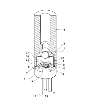
An embodiment will be explained by referring to the Figures. Fig. 1 is a
perspective view of a vertical section of the photodiode module as an embodiment of an
aspect of the present invention. This embodiment adopts a general-use three pin package
(1) of 5.6 mm diameter. This is a commonplace package which has been used for a
package of various kinds of transistors.
The package has three pins (10), (11) and (12). One pin is a case pin (10) whichis conn~cted to the package itself. Another pin is a source pin (11). The last pin is a
signal output pin (12) which transmits the signal of the preamplifier to an external circuit.
The case pin (10) is soldered to the package (1). Upper ends of the source pin (11) and
25 the signal output pin (12) project over the upper surface (5) of the package (1), the
source pin (11) and the signal output pin (12). The insulators merh~nic~lly hold the pins
(11) and (12) to the package (1), electrically separating the pins from the package (1).
A parallel plate capacitor (2) of a capacitance of 470 pF is fixed on the package
(1) with an AuSn (gold/tin) solder. The size of the rectangular capacitor (2) is
CA 02148894 1998-06-04
- 0.9mm X 1.0mm X 0.1mm. The parallel plate capacitor (2) has electrodes on the top
surface and the bottom surface (0.9mm X 1.0mm). The bottom surface is glued directly
with the AuSn solder to the package which is at the ground level. The AuSn solder has
a melting point of 286~C. The upper surface of the parallel plate capacitor (2) is another
5 electrode.
A photodiode (3) is positioned for harmonizing it with the center of the packageand is fixed on the parallel plate capacitor (2) with a SnPb solder. The melting point of
the SnPb (tin/lead) solder is 240~C. The difference of the melting points of the solders
is important for making the structure of Fig. 1. The solder which glues the bottom
10 surface of the parallel plate capacitor (2) to the upper face of the package (1) is called
the first solder. The melting point of the first solder is denoted by Tcl. The solder
which co~ e-;ls the bottom of the photodiode chip to the top of the parallel plate capacitor
(2) is called the second solder. The melting point of the second solder is denoted by
Tc2.
After the parallel plate capacitor (2) has been struck by the first solder to the
package (1), and the photodiode (3) is glued by the second solder to the top of the
parallel plate capacitor (2). The order of the soldering requires an inequality of
Tcl > Tc2. Otherwise, when the second solder is melted, the once-solidifled first solder
is also melted and the parallel plate capacitor is liable to displace from the normal
20 position.
The desirable difference (Tel-Tc2) of the melting points Tcl and Tc2 is more than
20~C. The above example satisfies the condition, because Tcl = 286~C, Tc2 = 240~C,
and Tcl-Tc2 = 46~C. There are other probable sets of solders in addition to the sets of
AuSn and SnPb of the example.
Fig. 16 exhibits the section of the mount of a parallel plate c~r~citor (2) and a
photodiode (3) on a package. A parallel plate capacitor (2) is stuck on a package (1)
with an AuSn solder (81). Since the parallel plate capacitor has a complete metal layer
(52) on the bottom, the whole of the bottom of the capacitor (2) is soldered to the upper
surface of the package (1). A photodiode (3) is glued with a SnPb solder (82) to the
30 upper surface (50) of the capacitor (2). The bottom of the photodiode (3) is
CA 02148894 1998-06-04
sllbst~n~i~lly-completely a metal electrode (91) which is an n-side electrode made from
gold (Au). The n-side electrode is directly soldered to the capacitor (2) with the SnPb
(82).
The bottom electrode (52) is allotted to the ground level and the top electrode (50)
is ~esign~d to the source voltage. A wire (21) connects the upper surface (50) to the
source pin (11).
The photodiode (3) is produced upon an n-type substrate. Many kinds of
photodiodes are available for this module. The substrate wafer is a crystal which can be
a substrate material of a photodetector, for example, a GaAs wafer, an InP wafer or a
Si wafer. The example of Fig. 16 consisl~ of a low resi~t~nce n-type substrate (92), a
buffer layer (93), a light-receiving layer (94) and a window layer (95) which are piled
in this order. A dish-shaped p-type region (96) is formed by thermal diffusion of a p-
type illlyulily at the centre of the upper surface. A ring-shaped p-side electrode (97) is
formed on the periphery of the p-type region (96). The peripheral in~ul~tor on the top
is a protective layer (99) which is made from SiN, SiO~, etc. The central tla~ alcnt
layer is an antireflection layer (98) which is made from multilayers of two materials with
different refractive indexes. The annular p-side electrode (97) which is an output of the
photodiode (3) is connPcted with a wire (23) to a preamplifier.
The preamplifier IC (4) is die-bonded at a peripheral point, as shown in Fig. 1
or Fig. 7. These parts are bonded on the package in the order of the parallel plate
capacitor (2), the preamplifier IC (4) and the photodiode (3). After the parts have been
bonded on the package, the parts, the print p~Uellls and the pins are joined by
wirebonding of gold (Au) wires of a 20 ~ m diameter.
As clearly demonstrated in Fig. 7, five wires (21) to (25) connect five sets 1) to
5) of pads or pins:
1) the source pin (11) and the upper surface of the parallel plate capacitor (2) by a wire
(21);
2) the upper surface of the parallel plate capacitor (2) and the source pad of the
preamplifier IC (4) by a wire (22);
CA 02148894 1998-06-04
19
3) the signal output pad (anode) of the photodiode (3) and the input pad of the
preamplifier (4) by a wire (23);
4) the output pad of the preamplifler IC (4) and the signal output pin (12) of the package
(1) by a wire (25); and
5) the ground pad of the preamplifier (4) and the package (19) by a wire (24).
A metal cap (7) with a lens (6) is fitted on the package (1) in an atmosphere ofdry nitrogen gas. The position of the cap (7) is determined at the spot which maximizes
the power of the vertically-incident light through the lens (6) into the photodiode (3).
Then, the cap (7) is welded by resistor welding at the spot on the package (1). Resistor
welding can be replaced by the laser welding. The inner space of the cap is
h~m~tic~lly-sealed by the welding.
Then a ferrule-holding sleeve (8) is positioned on the package (1). The optilllulll
position of the sleeve (8) is determined by inserting a fibre into the sleeve (8), sçn~ling
light in the ~lbre, observing the light power at the photodiode and ma~imi7ing the light
power. The sleeve (8) is fixed at the Optilllulll point by welding, that is, by YAG laser
welding or resistor welding. In the example, the sleeve (8) is fixed on the package (1).
The sleeve (8) can optionally be fitted on the cap (7).
The two-story structure of the PD and the capacitor enables aspects of this
invention to mount all the necessary parts within the central area of a 3.0 mm ~ mpt~r
on the package (1). This fact allows the device to use a general-purposed package of a
5.6 mm di~m~ter which is far smaller than the single-purposed packages of the prior art
devices (Fig. 5, Fig. 6 or Fig. 8).
Prior art modules were used to mount a capacitor and a photodiode at difrelelll
spots on a package. The flat structure dem~mled a wider area than an area of 4.0 mm
diameter for mounting the parts. Thus, prior art modules sometimes employed a 10mm
~i~mçter package or an 8mm diameter package. The prior structure required at least a
7mm diameter package owing to the flat distribution of the parts.
This invention in its various aspects succee~s in reducing the nl~cess~y area for
mounting parts of the package. The reduction of the mounting area enables aspects of
this invention to mini~ rize photodiode modules. The two-story mount of the module
CA 02148894 1998-06-04
dispenses with the incul~ting spacer of the photodiode which electrically in~ tes the
photodiode from the package. The omission of the spacer alleviates the number of the
parts and a number of steps of production.
The frequency pelrolmal1ce of the photodiode module which is driven by the
S signal rate of 125 Mbit/s is measured in order to estim~te the quality of the photodiode
module. Fig. 15 denotes the results. The frequency performance of the prior photodiode
module is also denoted in the same graph. The solid line shows the result of thephotodiode module of an aspect of this invention. The dotted line shows the plope~ly of
the prior art photodiode module. The abscissa is the frequency (MHz) of modulation,
10 while the ordinate is the output of the signal of the module in a unit of dB. The
photodiode of an aspect of this invention can accomplish a flat response property up to
more than lS0 MHz. The 3-dB ~tten-~tion frequency is 200 MHz.
The prior art photodiode module obtains a flat response prope,ly up to 90 MHz,
but suffers from a peaking at 100 MHz. The 3-dB ~ttenll~tion frequency is 130 MHz.
15 The result exhibits that the photodiode module of aspects of this invention enjoys more
excellent high frequency performance than the prior art photodiode module.
The above is an embodirnent which utilizes the capacitor (2) which is ~andwichedbetween the package (1) and the photodiode (3) in common both as a bypass c~paeitor
of the photodiode and as a bypass capacitor of the preamplifier. The capacitor can
20 alternatively solely be allotted to the bypass capacitor either for the photodiode or the
preamplifier.
Fig. 2 shows another embodiment of an aspect of this invention which makes use
of the capacitor as the bypass capacitor only of a photodiode. Instead of the three-pin
package, a four-pin package is employed in the second embodiment for sepalathlg the
25 source line of the photodiode from the source line of the preamplifier. Then, two
independent source pins are prepared in the package to the photodiode (3) and the
preamplifier (4), respectively. In this case, the parallel plate capacitor (2) is made use
of as a bypass capacitor solely for the photodiode (3). Fig. 2 is the perspective view of
the second embodiment and Fig. 10 is the circuit diagram of the same module.
CA 02148894 1998-06-04
21
In Fig. 2, a parallel plate capacitor (2) is soldered by the AuSn solder at the
center of the package (1). A photodiode (3) is soldered with the SnPb on the c~paeitor
(2). A preamplifier IC (4) is also soldered at a periphery of the package (1). The
bottom of the preamplifier (4) and the bottom of the capacitor (2) are at the ground level,
since they are directly bonded on the case (package) which is connected to the ground
pin (10). A PD source pin (11) is connected by a wire (21) to the upper surface of the
parallel plate capacitor (2). The preamplifier source pin (27) is joined by a wire (28) to
a source pad of the preamplifier (4). The source pins (11) and (27) are sepa,aled in
order to supply the photodiode (3) and the preamplifier (4) with dirre~e~ll voltages or
different DC impedance. The isolation of the photodiode (3) from the preamplifier (4)
is effective to cut the noise or to ~iUppleSs the parasitic oscillation. These are different
points from the former embodiment.
The other parts are the same as the first embodiment. An annular electrode (p-
side electrode) of the photodiode (3) is coupled by a wire (23) to an input pad of the
preamplifier (4). A signal output pad of the preamplifier (4) is joined by a wire (25) to
a signal output pin (12). A wire (24) connects a ground pad of the preamplifier (4) to
the case, (i.e., package (1)). An increase of the pin (27) hardly enlarges the size of the
package in the four-pin module.
This invention in its various aspects does not restrict the photodiode to an n-type
substrate one. A p-type substrate photodiode is also available in the module. In the case
of the p-type substrate photodiode, the voltage which is applied from the source is
negative. The polarities of parts are all reversed. A photodiode which has been built
on a semi-insulating semiconductor, for example, a GaAs photodiode, is also applicable.
In this case, no current flows throughout the substrate. Thus, the upper electrode of the
capacitor should be joined to the source pad of the photodiode chip. The module does
not restrict the driving voltage to 5 V. This invention in other aspects can be applied to
any device of any driving voltage.
Furthermore, this invention in yet other aspects is not confined to the 5.6mm
diameter package but can be applied to any sized package with any number of pins. This
.
CA 02148894 1998-06-04
~ .
22
invention, in its various aspects, narrows the mounting area on any package and reduces
the number of the parts.
The parallel plate capacitor can take various sizes and various shapes in various
aspects of this invention. The wire is not reskicted to gold (Au). Cu wires can be also
S utilized to connect the electrodes and pads in the module. The mode of conlle~;lion of
wires is not restricted to the mode shown in Fig. 1 or Fig. 2.
This invention succee-l~ in mi~ lion of a photodiode module and in
simplifying the steps of production of a photodiode module by piling a photodiode on a
parallel plate capacitor. The dirrerence of the nPcess~ry areas will easily be understood
10 by colnp~ing the plan views of the packages. Fig. 7 is the plan view of the package of
an aspect of the present invention. Fig. 8 is the plan view of the package of the prior
art module of Fig. 5. The comparison verifies the excellence of aspects of the present
invention.