Note: Descriptions are shown in the official language in which they were submitted.
214907
,~-..
INTEGRATED USER NETWORK INTERFACE DEVICE
FIELD
The present invention relates to a monolithic
integrated circuit that interface between synchronous
optical network (SONET)/synchronous digital hierarchy
(SDH) STS-3c, which is a digital transmission standard
that defines a new digital hierarchy for fiber optic
transmission and a frame structure for multiplexing
digital traffic, and asynchronous transfer mode (ATM).
ATM is a new payload multiplexing technique which
segments payload into 53-byte cells which can be
allocated to user channels based on demand.
BACKGROUND
The advent of applications such as network
computing, multimedia, video conferencing, and real-time
imaging require data rates ranging into the gigabits-per-
second. The demand for such high rates has led the
industry to combine a standardized wide band network
(SONET) with the simplicity of an efficient network that
uses fixed-length 53-byte-wide asynchronous transfer-mode
(ATM) cells. In 1992 ATM was chosen by the CCITT
(Consultative Committee for International Telephony and
Telegraphy and now the ITU) as the transport technology
for the huge variety of services to be offered by the
Broad band Integrated Services Digital Network (B-ISDN).
However, it has been recognized that ATM is equally well-
suited for use in the local area network. An ATM cell
consists of 53 octets or bytes with a 5 byte cell header
containing control bits and a 48 octet or byte cell
payload which contains the data bits. In order to
interface with a standardized wide band network, such as
Synchronous Optical Network (SONET), appropriate
interfaces to transfer from one system to the other have
been and are being developed.
-2- 214900
In order to integrate all of the functions of
an ATM physical layer interface into a single device, and
at the same time be applicable to local and wide area
networking applications, a number of criterion have to be
met. First, one requires a fully compliant SONET/SDH
STS-3c framer. Here the term SDH refers to ITU's
synchronous digital hierarchy and STS-3c refers to a data
-transmission rate of 155.52 megabits-per-second
(Mbits/s). The SONET STS-3c frame structure consists of
9 rows of bytes with each row having 9 bytes of transport
overhead and 261 columns of 9 bytes each with one of the
columns having control bits defining path overhead while
the remaining columns are payload. The framer takes ATM
cells and puts them into a synchronous series of SONET
frames.
A second requirement of an interface device is
an ATM cell processor to perform cell delineation and
null cell insertion/filtering. Since many of the
services delivered by ATM are by definition asynchronous,
they are characterized by a non-continuous cell stream.
Thus, cell rate de coupling transforms a non-continuous
cell stream into a continuous stream by inserting idle or
null cells (containing no payload) during idle periods in
the assigned cell stream. By making the cell rate
continuous, it is necessary only to synchronize with the
incoming cells in order to place the ATM cells in their
assigned locations in a frame.
A third requirement is a line side interface to
support serial input/output at 155 Mbits/s. For
SONET/SDH systems, current devices utilize expensive
external phase locked loops and crystal oscillators to
provide the clock recovery and clock synthesis functions.
No one to date has been able to successfully implement
integral phased locked loop circuits to recover clock and
data from the encoded incoming data stream and to
-3-
~2149~7~
synthesize the high speed transmit clock from a low
frequency reference.
Accordingly, it is an object of the invention to
provide an integral phase locked loop that recovers the
clock and data from the serial encoded receive stream and
that synthesizes the high speed 155.52 MHz or 51.84 MHz
transmit clock from a low frequency reference.
lO SUGARY OF THE INVENTION
According to the invention there is provided a
user network interface (UNI) device for interfacing between
a synchronous optical network (SONET) and an asynchronous
transfer mode (ATM) network. The UNI device has a transmit
section and a receive section. The transmit section is
operative to receive an incoming non-continuous stream of
data cells from the ATM network, generate and insert idle
cells into the incoming non-continuous stream of data cells
to form a continuous stream of cells, map the continuous
stream of cells into frames of data, and synchronously
transmit the frames of data in an outgoing continuous
stream of data. The receive section is operative to
receive incoming frames of data in an incoming continuous
stream of data, extract ATM cells from the incoming frames
of data, and transmit the extracted ATM cells in an
outgoing non-continuous stream of data cells. The receive
section includes an integral clock recovery circuit
operative to sample and recover clock from the incoming
continuous stream of data.
The integral clock recovery circuit is preferably
operative to lock on to and recover the clock from the
incoming continuous stream of data when a frequency
difference between a divided down output from the integral
clock recovery circuit and a first reference clock signal
is less than or equal to a predetermined threshold, and
-3A- 2 1 4 9 0 7 fi
where otherwise the integral clock recovery circuit locks
on to the first reference clock signal.
The integral clock recovery circuit is also preferably
operative to lock on to and recover the clock from the
incoming continuous stream of data only if the incoming
continuous stream of data has a number of transitions
greater than or equal to a preset value for an n-bit
interval. In one embodiment, the preset value is 1 and the
n-bit interval is an 80-bit interval.
Preferably, the integral clock recovery circuit
includes a first voltage control oscillator (VCO) operative
to lock on to the incoming continuous stream of data, a
phase/frequency detector operative to compare the phase and
frequency of a first reference clock signal and the divided
down VCO output signal from a first divider circuit, and a
data phase detector operative to compare the phase of the
incoming continuous stream of data and the divided down
output signal from the first divider circuit. Preferably,
the first VCO is switched from the phase/frequency detector
to the data phase detector when a frequency difference
between a frequency of the divided down output signal from
the first VCO and that of the first reference clock signal
is less than or equal to a predetermined threshold, and the
first VCO is switched back to the phase/frequency detector
when the frequency difference exceeds the predetermined
threshold.
The integral clock recovery circuit may include a
first reference clock input line for receiving a first
reference clock signal and a data input line for receiving
the incoming continuous stream of data. The clock recovery
circuit may also include a first loop filter operative to
cut out high frequency components of input signals and to
control input of the first VCO, a loop control multiplexer
operative to selectively drive the loop filter and control
r
-38- 2 1 4 9 0 7 fi
the first VCO from one of the phase/frequency detector and
the data phase detector, a transition detector operative to
monitor a transition density of the incoming continuous
stream of data, a clock difference detector, operative to
compare a frequency of the first reference clock signal and
the divided down output signal of the first VCO, and a
control state machine operative to control the control loop
multiplexer.
As contemplated within the scope of this
invention, there is also provided a user network interface
device comprising a transmit section and receive section
wherein the receive section includes an integral clock
synthesis circuit operative to synthesize a high speed
transmit clock from a low frequency reference source.
Preferably, the integral clock synthesis circuit includes a
second voltage control oscillator (VCO); a second divider
circuit having an input coupled to an output of the second
VCO; (cc) a second loop filter having an output coupled to
an input of the second VCO; (dd) a charge pump coupled to
the second loop filter and operative to send source
currents and sink currents into the second loop filter to
control the second VCO; (ee) a second reference clock line
for receiving a second reference clock signal; and (ff) a
dual phase/frequency detector operative to drive the charge
pump, having an input coupled to an output of the second
divider circuit and the second reference clock line.
The second loop filter may have a transfer
function optimized to enable the integral clock synthesis
circuit to track the second reference clock signal and
attenuate high frequency fitter on the second reference
clock signal. The transfer function may yield a low pass
corner frequency of about 736 KHz when referenced to a
19.44 MHz crystal. The transfer function may also yield a
low pass corner frequency of about 245 KHz when referenced
to a 6.48 MHz crystal.
r
-3C-
2 14 9076
In another embodiment, the transmit section of
the UNI device comprises (i) a transmit cell buffer
operative to receive and store incoming data cells from the
incoming non-continuous stream of data cells; (ii) a
transmit section processor operative to generate and insert
idle cells into the incoming non-continuous stream of data
cells to form a continuous stream of cells and to map the
continuous stream of cells into outgoing frames of data,
the transmit section processor having an input coupled to
an output of the transmit cell buffer; (iii) a parallel-to-
serial converter having an input coupled to an output of
the transmit section processor; (iv) an encoder, having an
input coupled to an output of the parallel-to-serial
converter, operative to encode data received from the
parallel-to-serial converter; and (v) an integral clock
synthesis circuit coupled to the encoder and operative to
synthesize a high speed transmit clock from a low frequency
reference source; wherein the receive section transmits the
outgoing frames of data in an outgoing continuous stream of
data directed to the synchronous optical network. In this
embodiment, the receive section is operative to receive
incoming frames of data in an incoming continuous stream of
data from the synchronous optical network and comprises:
(i) a serial interface; (ii) a decoder operative to recover
data from the incoming continuous stream of data and having
an input coupled to the serial interface; (iii) an integral
clock recovery circuit operative to sample and recover
clock from the incoming continuous stream of data, having
an output coupled to an input of the decoder; (iv) a
serial-to-parallel converter having an input coupled to an
output of the decoder; (v) a receive section processor
operative to extract data cells from the incoming frames of
data, having an input coupled to an output of the serial-
to-parallel converter; and (vi) a receive cell buffer
operative to store the extracted data cells for
transmission in an outgoing non-continuous stream of data
cells, having an input coupled to an output of the receive
ax ~
-3D- 2 1 4 9 0 7 6
section processor; wherein the receive section transmits
the extracted data cells in an outgoing non-continuous
stream of data to the ATM network.
As also envisioned within the scope of this
invention, there is provided a method, in a user network
interface (UNI) device interfacing between a synchronous
optical network (SONET) and an asynchronous transfer mode
(ATM) network, for recovering clock from an incoming
continuous stream of data received by the UNI device from
the synchronous optical network, the UNI device having an
integral clock recovery circuit. In one embodiment the
method comprises the steps of:
(a) generating a divided down clock signal in the UNI
device;
(b) testing if a frequency of a reference clock
signal and a frequency of the divided down clock signal
differs by no more than a predetermined threshold;
(c) synchronizing the integral clock recovery circuit
to a phase and a frequency of the incoming continuous
stream of data, if the test in step (b) produces a result
of true; and
(d) recovering clock from the incoming continuous
data stream in the event the phase and frequency are
synchronized in step (c).
In another embodiment, the method for recovering
clock from an incoming continuous stream of data comprises
the steps of:
(a) driving a first voltage control oscillator (VCO)
in the integral clock recovery circuit with a
phase/frequency detector;
(b) dividing down a signal from the first VCO to
produce a divided down clock signal;
r l
-3E- 2 1 4 9 0 ~ 6
(c) testing if a frequency of a reference clock
signal and a frequency of the divided down clock signal
differs by no more than a predetermined threshold;
(d) switching control of the first VCO from the
phase/frequency detector to a data phase detector so as to
synchronize to a phase and a frequency of the incoming
continuous stream of data, when the test in step (c)
produces a result of true;
(e) testing if the incoming continuous stream of data
has a number of transitions greater than or equal to a
preset value for an n-bit interval; and
(f) signaling to the UNI device that the integral
clock recovery circuit is locked on to the clock of the
incoming continuous stream of data in the event the phase
and frequency are synchronized in step (c) and the number
of transitions is greater than or equal to the preset value
in step (e).
There is also contemplated within the scope of
this invention a method, in a UNI device, of synthesizing
with a integral clock synthesis phase lock loop circuit a
high speed transmit clock from a low frequency reference
source. This method may include the steps of:
(a) controlling a second voltage control oscillator
(VCO) with a charge pump;
(b) generating a divided down output signal from the
second VCO with a second divider circuit;
(c) comparing the divided down output signal to a
second reference clock signal; and
(d) driving the charge pump with a dual
phase/frequency detector so as to synchronize the divided
down output signal with the second reference clock signal.
-4- : 2 14 9076
BRIEF DESCRIPTION OF THE DRA~TINGS
The novel features believed characteristic of the
invention are set forth in the appended claims. The
invention itself, as well as other features and advantages
thereof, will be best understood by reference to the
description which follows read in conjunction with the
accompanying drawings, wherein:
FIG. 1 is a schematic diagram of the SONET/SDH
ATM physical layer interface;
FIG. 2 is a schematic diagram of the ATM cell
structure;
FIG. 3 is a schematic diagram of a SONET STS-3c
frame structure;
FIG. 4 is a schematic diagram of an application
of the user network interface device coupled on its line
side to a line receiver/equalizer and a line driver and on
the other side to ATM layer processors;
FIG. 5 is a schematic diagram of an 8 bit ATM
cell structure;
FIG. 6 is a transmit logical timing diagram;
FIG. 7 is a receive timing diagram for a single
physical layer device;
FIG. 8 is a receive timing diagram for a multiple
physical layer configuration;
-5- 2 14 9076
FIG. 9 is a cell delineation state diagram;
FIG. 10 is an HCS verification state diagram;
FIG. 11 and FIG. 11a are a schematic diagram of
clock recovery circuit; and
FIG. 12 and FIG. 12a are a schematic diagram of
the clock synthesis circuit.
DETAILED DESCRIPTION WITH REFERENCE TO THE DRAWINGS
Referring to Figure 1 the user network interface
device or physical layer device 10 implements the SONET/SDH
processing and ATM mapping functions of a 155 Mbit/s or 51
Mbit/s ATM user network interface. SONET/SDH frames are
received on receive differential data inputs RXD+ and RXD_
by the bit serial interface 11. The output from the bit
serial interface 11 is directed to decoder 16 which
recovers data and couples to the clock recovery circuit 13
which recovers the clock. The output from the decoder 1 6
is directed to a serial-to-parallel converter 18 which
converts the received 155.52 Mbit/s SONET stream to a 19.44
Mbytes stream and searches for the SONET/SDH framing
pattern in the incoming stream and performs serial to
parallel conversion on octet boundaries.
The output of the serial to parallel converter
18 is coupled to the input of a receive framer and overhead
processor 20 which provides frame synchronization, de-
scrambling, pointer interpretation, extraction of path
overhead, extraction of the synchronous payload envelope
(SPE), detection of section, line and path level alarm
conditions, monitoring section, line and path bit
interleaved parity, and accumulating error counts at each
level for performance monitoring purposes.
2I4~O~~i
Following overhead processing,
the signals from
the output of the processor 20 are directed to the input
of a receive ATM cell processor
23. The ATM cell
processor 23 performs framing to the ATM payload using
ATM cell delineation with cell filtering based on
idle/unassigned cell detection and header check sequence
error detection, and performs
ATM cell payload de
scrambling. Idle/unassigned cells may be dropped
according to a programmable filter. Cells are also
dropped upon detection of an uncorrectable header check
sequence error. The ATM -cell payloads are descrambled.
Generic flow control (GFC) bits
from error free cells are
extracted and presented on a serial link for external
processing. The output of the receive ATM cell processor
23 couples to the input of a 4 cell deep receive ATM cell
FIFO 26 which passes data structures consisting of
53 8-bit words and is used to
separate the STS-3c line
timing from the higher layer ATM system timing. Cells
are read from the output of th e FIFO 26 by a synchronous
8 bit wide data path interface with cell-based handshake.
A transmit cell FIFO 30 provides FIFO
management and the asynchronous interface between the
physical layer device 10 and the external environment.
The transmit FIFO 30 can accommodate four cells. It
provides for the separation of the STS-3c line or
physical layer timing from the ATM layer timing. The
FIFO 30 supports 53 8-bit words, comprising the 5 octet
cell header, and the 98 octet payload.
Management functions of the transmit FIFO 30
include filling the transmit FIFO 30, indicating when
cells are available to be written to the transmit FIFO
30, maintaining transmit FIFO read and write pointers,
and detecting a FIFO overrun condition. Upon detection
of an overrun condition, the FIFO 30 is automatically
;,,~ -' - 2 1 4 9 0 7 6
reset . Up to four cells may be lost during the FIFO reset
operation. FIFO overruns are indicated through a maskable
interrupt and register bits. The synchronous interface
provided to an external device (not shown) issues a TSOC
signal to indicate to the FIFO 30 that the first word of
the selected data structure is present on the TDAT bus.
The external circuitry is then notified by issuance of a
TCA signal that a cell may be written to the transmit FIFO
30 (cell available). Once the cell is written to the FIFO
30, the FIFO 30 changes from cell available to cell
unavailable status on write cell boundaries.
The Transmit Cell Processor 32 coupled to the
output of the FIFO 30, provides rate adaptation via
idle/unassigned cell insertion and HCS generation and
insertion, and performs ATM cell scrambling. An idle or
unassigned cell is transmitted if a complete ATM cell has
not been written into the FIFO 30.
The transmit framer and overhead processor 3 4
has an input coupled to the output of the cell processor
32. The transmit overhead processor 34 provides transport
frame alignment generation, pointer generation, path
overhead insertion, insertion of the synchronous payload
envelope, insertion of path level alarm signals and a path
bit interleaved parity calculation and insertion for
performance monitoring.
Transmit line overhead processing provides line
level alarm insertion, and bit interleaved parity insertion
using even parity as required to allow performance
monitoring on the far end. Line and path far end block
error indications are also inserted. Transmit section
overhead processing provides frame pattern insertion,
scrambling, section level alarm signal insertion and bit
interleaved parity insertion.
_$_
2~4907~
The output from the transmit framer and
overhead processor 34 is directed to a parallel to serial
converter 37 which converts the internal 19.44 Mbytes
stream to a 155.52 Mbit/s stream which it directs to
encoder 36. Encoder 36 scrambles the payload of ATM
cells although such scrambling can be disabled.
No line rate clocks are required directly by
the device 10 as it synthesizes the transmit clock and
recovers the receive clock using a 19.44 MHz or 6.48 MHz
reference clock.
Referring to Figure 2 there is shown an ATM
cell structure which consists of 53 octets or bytes. A
cell header 11 has 5 octets and the cell payload has 48
octets. The cell header fields are shown in Figure 2.
The GFC consists of four bits which contain the generic
flow control field and are used for traffic flow control
of the user network interface (UNI). The VPI/VCI fields
consist of 24 bits containing the virtual path/virtual
channel identification. These fields are used for
routing a cell through a private or public ATM network.
The PT field consists of three bits indicating the
payload type carried by the cell. The eight values
represented by this field are used to indicate the cell
user data type, and management information. The CLP
field contains one bit which allows the user or the
network to set the loss priority of the cell. This bit
is set for cells that may be discarded by the network.
The field HEC called the header error control octet is
used by the physical layer for cell delineation. It is
also used for detection and correction of bit errors in
the cell header. This octet or byte is also referred to
as the header check sequence (HCS).
2~4907~
-9-
Referring to Figure 3 there is shown the frame
structure for a SONET STS-3c transmission format. In
North America, the SONET standard (ANSI T1.105) was
initially released in 1988. The commonly defined
interfaces and their associated rates are listed below:
Interface Rate (~it/a)
STS-1 51.84
STS-3/STS-3c 155.52
STS-12/STS-12c 622.08
STS-48 2488.32
Referring to Figure 3 there is shown the SONET
STS-3c frame structure which consists of 9 rows by 9
columns of transport overhead byte positions, one column
of 9 bytes of path overhead and 260 columns of
synchronous payload envelope in which ATM cells are
placed horizontally and contiguously. Not all of the
bytes in the transport overhead are filled. Some of the
more important fields are A1 and A2 which specify the
frame alignment pattern. In its transmit mode the device
10 inserts the frame alignment pattern (F6F6F6282828H)
where the capital letters are the well-known hexidecimal
symbols . In the receive mode the device 10 searches the
data stream for the SONET frame alignment pattern. When
the pattern has been detected for two consecutive frames,
the device declares in-frame. When errors are detected
in the pattern for four consecutive frames, the device
declares out-of-frame.
Field B1 is the Section Bit Interleaved Parity
which contains an 8-bit interleaved parity calculated
across the entire SONET frame of 2430 bytes. The B1
value is calculated based on even parity, and the value
inserted in the current frame is the parity value
calculated for the previous frame.
2~499'~~
-10-
H1, H2, H3 are the payload pointer which, in
the transmit direction, may be fixed and in the receive
direction is interpreted to locate the J1 byte which
represents the first byte of the synchronous payload
envelope (SPE). It is used to accommodate the fitter and
wander that accumulates in all transmission systems.
Pointer movements cause the SPE to move within the SONET
frame 3 bytes at a time.
The field B3 is a path 8-bit interleaved parity
calculated across the entire synchronous payload
envelope.
The field H4 is the ATM Cell Offset which in
the transmit direction indicates the offset in bytes to
the next ATM cell boundary in the transmit stream. The
byte can be used to delineate cell boundaries in the
receive stream. However, cell delineation techniques
that use the HEC octet are preferred.
Referring to Figure 4, the device 10 couples a
fibre optic line system 43 with an ATM terminal 42. On
the line side an optical receiver 44 receives light
signals generated by a remote laser (not shown) and
converts them to electrical signals in SONET/SDH frames.
The frames are processed by the device 10 which then
transmits to the ATM Terminal 42 in the form of ATM
cells. It recovers the 155.52 Mbit/s clock signal from
the received frames and uses this clock to transmit to
the optical transmitter 46. ATM cells received by the
device l0 are processed and placed in transmitter 46.
Cell Rate De coupling
ATM cells may be passed to/from the ATM cell
FIFO 30 using a defined data structure, namely, a 9-bit
structure consisting of a start of a cell indication, and
an 8-bit wide word as shown in Figure 5. Here H1 to H5
-l- 214J0'~~
contain the ATM cell header. Words 6 to 53 contain the
ATM cell payload.
Because the ATM cells are asynchronous whereas
the SONET/SDH frames are sent at 155.52 Mbit/s, in order
to go from one transmission mode to the other, it is
necessary to decoupage the timing for the data in one
mode from that in the other.
In going from ATM to SONET/SDH, the ATM cells
arrive at the transmit side of the ATM cell FIFO 30 at
irregular intervals. Consequently, a buffer must be used
to temporarily store bytes so that they can then be read
out from the buffer at a rate which is synchronized to
the desired bit rate for SONET/SDH of 155.52 Mbit/s.
In this case, the buffer is a transmit four
cell FIFO 30. ATM cells are stored in the transmit FIFO
30. When FIFO 30 has space for a cell it first sends out
a transmit cell available signal (TCA) to notify the
external circuitry that a cell may be written to the
transmit FIFO 30. To accomplish this, as shown in the
timing diagram of Figure 6, the TCA output transitions
from 0 to 1 on the rising edge of the transmit FIFO clock
signal TFCLK when the transmit FIFO 30 contains one empty
cell. TFCLK is used to synchronize data transfer
transactions from an external ATM layer device (not
shown). A transmit write enable signal (TWRENB) is used
by an external ATM layer device (not shown) to indicate
to the device 10 the cycles in which the transmit data
(TDAT) on the TDAT bus, the transmit parity (TXPRTY) and
the transmit start of cell (TSOC) signals contain valid
data. When TWRENB is sampled low by the device 10,
interchange data is considered valid. When TWRENB is
sampled high by the device 10, interchange data is
considered invalid and no transfer is performed. As
shown in Figure 6, there is an additional signal transmit
-12-
21~+9476
write address bus (TWRAD) which is utilized only for multi-
physical layer device applications. It is used to address
individual physical layer devices 10 from the external ATM
layer device (not shown). The logical timing shown is
valid for both single and multiple physical layer operating
modes. ln~hen TCA is deasserted and it has been sampled, the
ATM layer device (not shown) can write no more than four
bytes or words to the physical layer device 10. If the
ATM layer device writes more than four words and the TCA
remains deasserted throughout, the physical layer device
will indicate an error condition and ignore additional
writes until it asserts TCA again.
Going from SONET/SDH to ATM, ATM cell boundaries
must be located in the synchronous payload envelope of each
frame, verified and the cells placed in the receive FIFO
26 . These cells are then read out of the receive FIFO 2 6
to external ATM circuitry in response to an active receive
read strobe signal from this external circuitry. The data
path between an ATM layer and present physical layer device
10 is an 8 bit data path. Clock rates of up to 33 MHz are
supported. Transmit and receive data transfers at clock
rates independent of line bit rate are achieved using cell
rate de coupling using FIFO's 26 and 30. Control signals
are provided to both the ATM layer (not shown) and the
physical layer device 10 to allow either one to exercise
flow control, although normally the physical layer device
10, being at the lowest protocol layer, should operate as a
slave.
In the receive direction, as shown in Figures 7
and 8, when the physical layer device 10 has accumulated a
cell in its receive FIFO 26, it informs the ATM layer
device that a cell is available to be read by asserting a
receive cell available signal RCA. The ATM layer device
A
-13- 2~490'~0
',..,
can then request at least 53 bytes (8 bit mode) from the
physical layer device 10 by asserting an enable
signal(RRDENB). Receive FIFO clock (RFCLK) cycles at 25
MHz or lower and is used to synchronize data transfer
transactions from the physical layer device 10 to an
external ATM layer device (not shown). When RRDENB is
sampled low by the physical layer device 10, the receive
data (RDAT), the receive parity (RXPRTY) and receive
start of cell (RSOC) signals will be accepted by the ATM
layer device (not shown) on the next rising edge of
RFCLK. When RRDENB is sampled high by the physical layer
device 10, no transfer is performed in the subsequent
RFCLK cycle. As seen for the single physical layer case,
RCA remains high until the internal FIFO of the physical
layer device is empty. The ATM layer device (not shown)
indicates, by asserting the RRDENB signal, that the data
on the RDAT bus during the next RFCLK cycle will be read
from the physical layer device 10. When the last word of
the last cell is available on the RDAT bus, RCA
transitions low. Once RCA is deasserted and has been
sampled, the ATM layer device (not shown) can issue no
additional reads. If the ATM layer device issues more
reads than the allowable number, the RCA remains
deasserted throughout, the physical layer device 10 will
indicated the condition and ignore the additional reads.
During multiple physical layer devices mode of operation,
several physical layer devices share the RDAT, RSOC and
RXPRTY signals. As a result, these signals must be tri-
stated in all physical layer devices which have not been
selected for reading by the ATM layer (not shown).
Selection of which physical layer device is being read is
made via dedicated RRDENB signals, or by the encoded
physical layer device selection address (RRDAD) in
conjunction with a multiple physical layer device read
enable signal (RMPRDENB). Figure 8 shows the timing
diagram for the multiple physical layer device near empty
mode.
-14- ~1490~0
In the transmit direction, when the physical
layer device 10 has space for a cell in its transmit FIFO
30, it informs the ATM layer device by asserting a
transmit cell available signal (TCA). The ATM layer
device can then write at least 53 bytes (8 bit mode) to
the physical layer device 10 using an enable signal
(TWRENB). For both transmit and receive interfaces the
ATM layer device 10 can at any point suspend the transfer
by deasserting its enable signal
Because in SONET or SDH a continuous stream of
cells is transmitted in sequence, whereas in ATM the cell
stream is non-continuous, transforming a non-continuous
cell stream into a continuous one requires inserting idle
or unassigned cells during idle periods in the assigned
cell stream. Consequently, in going from SONET to ATM it
is necessary to recognize and discard these idle cells.
This is done by simply testing the header pattern to
determine if it is in the format for an unassigned cell.
In the present case the first four octets or bytes in the
header will each be OOH if the cell is idle or
unassigned.
ATM Cell Delin~ation
Cell delineation is the process of framing to
ATM cell boundaries using the header check sequence (HCS)
field found in the cell header. The HCS is a cyclic
redundancy check calculation over the first 4 octets of
the ATM cell header (see Figure 2). When performing
delineation, correct HCS calculations are assumed to
indicate cell boundaries. Cells must be byte aligned
before insertion in the synchronous payload envelope.
Thus, a cell delineation algorithm can search the 53
possible cell boundary candidates one at a time to
determine a valid cell boundary location. While
searching for the cell boundary location, the cell
-ls- 2I4907~
,~,..~
delineation circuit is in the HUNT state 60 shown in
Figure 9. When a correct HCS is found, a cell
delineation state machine (not shown) locks on the
particular cell boundary and enters the PRESYNC state 62.
s This PRESYNC state 62 validates the cell boundary
location. If the cell boundary is invalid then an
incorrect HCS will be received within the next DELTA
cells, at which a transition back to the HUNT state 60 is
executed. DELTA is a value to be selected. If no HCS
errors are detected in this PRESYNC state 62 then the
SYNC state 64 is entered. While in the SYNC state 64,
synchronization is maintained until a ALPHA consecutive
incorrect HCS patterns are detected, where ALPHA is a
value to be selected. In such an event a transition is
is made back to the HUNT state 60 is executed. The values
of ALPHA and DELTA determine the robustness of the
delineation method. ALPHA determines the robustness
against false misalignments due to bit errors. DELTA
determines the robustness against false delineation in
the synchronization process. ALPHA is chosen to be 7 and
DELTA is chosen to be 6. These values result in a
maximum average time to delineate of 31 microseconds.
Cells are filtered based on HCS errors and/or a
2s cell header pattern. Cell filtering is optional and is
enabled through the registers (not shown) of the Receive
ATM cell Processor 23. Cells are passed to the receive
FIFO 26 while the cell delineation state machine is in
the SYNC state 64 as described above. When both
filtering and HCS checking are enabled, cells are dropped
if uncorrectable HCS errors are detected, or if the
corrected header contents match the pattern contained in
the 'Match Header Pattern' and 'Match Header Mask'
registers. Idle or unassigned cell filtering is
3s accomplished by writing the appropriate cell header
pattern into the 'Match Header Pattern' and 'Match Header
Mask' registers. Idle/Unassigned cells are assumed to
-16-
2 ~4 90~ s
contain the all zeros pattern in the VCI and VPI fields.
The 'Match Header Pattern' and 'Match Header Mask'
registers allow filtering control over the contents of the
GFC, PTI, and CLP fields of the header. The HCS is a
cyclical redundancy check calculation over the first 4
octets of the ATM cell header. The RACP block verifies the
received HCS using the polynomial, x8 + x2 + x + 1. The
coset polynomial, xs + x° + x2 + 1 is added (modulo 2) to
the received HCS octet before comparison with the
calculated result. V~hile the cell delineation state
machine (referred to above) is in the SYNC state 64, the
HCS verification circuit implements the state diagram shown
in Figure 10. In normal operation the HCS verification
state machine remains in the 'Correction Mode' state 66.
Incoming cells containing no HCS errors are passed to the
receive FIFO 26 (of Fig. 1). Incoming single bit errors
are corrected, and the resulting cell is passed to the FIFO
26. Upon detection of a single bit error or a multi-bit
error, the state machine transitions to the 'Detection
Mode' state 68. In this state, the detection of any HCS
error causes the corresponding cell to be dropped. Cells
containing an error-free HCS are passed, and the state
machine transitions back to the 'Correction Mode' state 66.
Clock Recovery
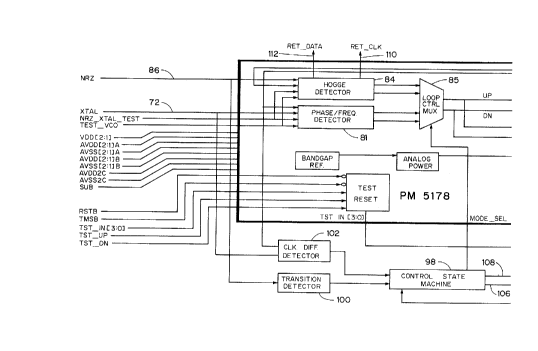
Referring to Figure 11 and 11a, clock recovery
unit 80 recovers the clock from the incoming bit serial
data stream. Unit 80 utilizes an external low frequency
reference clock signal XTAL on line 72 to train and monitor
its voltage controlled oscillator (VCO) 82 associated with
its clock recovery phase lock loop. The VCO 82 is a linear
voltage -to-current converter (Sedra current conveyor)
followed by a current-controlled relaxation oscillator. The
VCO 82 operates nominally at 155.52 MHz frequency. The
wide adjustment range guarantees that over process and
temperature the VCO 82
-17-
2149076
is always able to operate at 155.52 MHz. The maximum
operating frequency of the VCO 82 is 340 MHz under all
operating conditions. The VCO 82 design is optimized for
minimum intrinsic fitter generation. In training mode
where rapid frequency acquisition is required, the three
state phase/frequency detector 81 compares the phase and
frequency of the reference clock signal XTAL 72 and the
divided down VCO output DCLK 104. Detector 81 has the
characteristic that it is always guaranteed to correctly
drive the loop filter and VCO 82 towards a true lock
condition, regardless of the operating frequency range and
gain of the VCO 82. Detector 81 pulls the VCO 82 towards
the nominal SONET STS-N operating frequency by locking onto
the signal XTAL line 72 generated by an off board crystal
reference oscillator (not shown). The XTAL signal on XTAL
line 72 provides reference rates of 19.44 MHz and 6.48 MHz.
Once the VCO frequency differs from the nominal operating
frequency by less than 244 ppm, a Hogge detector 84 is
switched in as the phase detector. The Hogge 84 compares
the phase of edges in the serial data input stream and the
divided down VCO output. The Hogge detector 84 has the
characteristic that if the serial data input stream is
scrambled (i.e. pseudo-random with 50~ ones density), and
its bit gate is within 244 ppm of the divided down VCO
output clock frequency, the Hogge detector 84 correctly
drives the loop filter and VCO 82 towards lock condition.
The Hogge detector 84 also samples the serial data input
stream, on NRZ 86 in the center of the eye and generates
phase aligned clock and retimed data outputs, RET_CLK 1 1 0
and the center of the RET DATA 112. The maximum deviation
between the rising edge of RET_CLK 110 and the center of
the RET_DATA pulse width is less than 13 degrees or 0.072
UI peak. The Hogge detector 84 acts as synchronizer and
decision maker allowing data and clock to be recovered from
the incoming non-return to zero (NRZ) input signal 86.
Clock recovery unit 80 is robust in its ability to tolerate
-1g- ~. 2 14 90~ s
input fitter and is optimized for very low fitter transfer.
Divider circuits 88 and 90 provide division by 8 and 24
for the training aspect of the phase lock loop and division
by 1, 3, 6, and 12 for the recovery side. The VCO 8 2
operates at 155.52 MHz in all configurations. Loop
bandwidth varies from 240 KHz to 10 KHz corresponding to
cases N=1 and N=24 (the divider ratio between the output
and the inputs of the phase locked loop).
The phase detectors 81 and 84 produce correction
pulses that determine whether the VCO 82 is running too
fast or too slow. These correction pulses are filtered by
an active RC filter whose dynamics are optimized to meet
and exceed SONET fitter requirements. The passive filters
(not shown) that provide feedback around the op amp present
in the active filter section of the loop filter 94 are
provided externally.
Phase detectors 81 and 84 feed into a loop
control multiplexer 85 which selects whether the data
recovery phase detector 84 or the reference phase/frequency
detector 81 is used to drive the loop filter and control
the VCO 82. The loop control multiplexer 85 is controlled
by the external control state machine 98.
The output of loop control multiplexer 85 goes
to a loop filter 94 shown in Figures 11 and 11a which cuts
out the high frequency components of the phase detector
outputs and generates the controlling input of the VCO.
The passive network on the input side R1, C1 introduces a
higher order pole for blocking spurious modulation noise.
The ratio of R2 to R1 sets the midband gain
287/26.6K=0.011. The series connected R2, C2 pairs are
external to the chip.
A
- 19-
2 14 907 fi
The transition detector 100 monitors the input
data stream on the NRZ input and determines whether the
transition density is adequate for clock recovery purposes.
The transition detector 100 notifies the control state
machine 98 if no transitions are present for an interval of
80 bits.
The clock difference detector 102 compares the
frequencies of the signals on XTAL line 72 and DCLK 104.
Comparisons are done over intervals of 4096 cycles of the
signal on XTAL line 72. In each such interval the number
of cycles of the signal on DCLK 104 is counted. If this
count differs by more than 1, then the control state
machine is notified that the signal on XTAL line 72 differs
by more than 244 ppm; otherwise, the control state machine
98 is notified that the signals on XTAL line 72 and DCLK
104 differ by less than 244 ppm.
The outputs of the clock difference detector 102
and transition detector 100 are directed to the control
state machine 98. The control state machine 98 determines
whether clock is recovered from the NRZ input 86 or
synthesized from the signal on the XTAL input 72. The
control state machine 98 operates the loop control mux 8 5
and drive the DOOL 10 6 and ROOL 10 8 outputs that indicate
the status of the device. Upon release of reset, the
control state machine 98 forces the loop control mux 85
such that the phase lock loop is referenced to the XTAL
signal on XTAL line 72. The DOOL output 106 is forced
high indicating that the VCO 98 is not locked to data. The
ROOL output 108 is forced high indicating that the VCO 9 8
is not yet locked to the signal on XTAL line 72. In time
the VCO 98 will lock to the signal on XTAL line 72 and the
clock difference detector notifies the control state
machine 98 that the inputs to the phase/frequency detector
81 differ by less than 244 ppm. At this point the control
state machine 98
-20-
2 ~4 90~ s
will force the ROOL output 108 low, indicating that the
VC0 82 is locked to the signal on XTAL 72 and thus trained
to within 244 ppm of the nominal SONET/SDH bit rate
expected on the NRZ input 86.
Once the VCO 82 is locked to the reference, the
control state machine 98 waits until the transition
detector 100 indicates that the transition density is high
enough (no more than eighty consecutive ones or zeros) on
the NRZ input signal 86. Then the control state machine
98 switches the loop control mux 85 over the Hogge
detector 84. At this point, the DOOL output is forced low
indicating that the VCO 82 is locked to data. While the
VCO 82 is locked to data, the control state machine 9 8
continues to monitor transition density on NRZ and
frequency offset between the signal on XTAL line 72 and
DCLK 104 .
If the transition detector 100 indicates that
transition density is poor (more than eighty consecutive
ones or zeros occur), then the control state machine
switches the loop control mux 85 such that the VCO 82 is
once again controlled by XTAL on XTAL line 72. At this
point DOOL 106 is forced high. ROOL 108 is forced to
remain low until an interval passes that is adequate to
allow the VCO 82 to lock to the XTAL signal on XTAL line
72. Then the VCO 82 is once again considered trained to
the reference, or determined to be out of lock, at which
point ROOL 108 would be brought high. Once the VCO 82 is
trained to the XTAL signal on XTAL line 72, the control
state machine 98 again determines when to switch to
tracking data on NRZ 86.
Similarly, if the clock difference detector
indicates that DCLK 104 and the XTAL signal on XTAL line
72 differ by more than 244 ppm, then the control state
machine 98 switches the loop control mux 85 such that the
-21 -
2 1 4 9 (~ 7 ~
VCO 82 is once again controlled by XTAL 72. At this point
DOOL 106 is forced high. ROOL 108 is forced to remain low
until an interval passes that is adequate to allow the VCO
82 to lock to XTAL signal on XTAL line 72. Then the VCO
82 is once again considered trained to the reference, or
determined to be out of lock at which point ROOL 108 would
be brought high. Once the VCO 82 is trained to the XTAL
signal on XTAL line 72, the control state machine 98 again
determines when to switch to tracking data on NRZ 86.
10.
External blocks consist of a divide-by-8 9 0
which is a synchronous counter, a test decoder 96 which is
a test circuitry decoding block, a transition detector 1 0 0
which is a synchronous counter, a frequency difference
detector 102 which is a synchronous counter, a control
state machine 98, a decoder circuit 96 for setting
operating modes and active filter passives, the resistive
and capacitive elements accompanying the op amp based loop
filter 94. The divide-by-8 circuit 90 interfaces with the
internal divide-by-3 circuit 88 to generate feedback
signals for both sides of the loop. A test decoder 9 6
sets up diagnostic and production test setups within the
circuit 80 when in test mode (TMSB=0). The state machine
98 determines whether the loop is in training mode or
recovery mode. The transition detector 100 and frequency
difference detector 102 supply state machine 98 with
signals relating the state of the loop at any given time.
The off-chip passives consist of two resistors and two
capacitors (not shown).
When in reset (RSTB=0) the VCO is shut off by
grounding the integrating capacitor in the active loop
filter. The frequency difference detector 82 is shut off
by grounding the integrating capacitor (see Figure 11 and
11a) in the active loop filter 94. The frequency difference
detector 82 sends the loop in training mode by forcing
-22-
~''
2 14 90'~ 6
the state machine output MODE SEL low. The Data Out of
Lock (DOOL) 106 and Range Out Of Lock (ROOL) 108 outputs
on the state machine 98 both go high. Once the frequency
of DCLK 104 is within 244 ppm of the reference frequency
on XTAL line 72, ROOL 108 goes low and the loop switches
over to recovery mode. Once the Hogge detector 84 acquires
phase lock, DOOL 106 goes low and error free data recovery
begins.
Clock Synthesis
Referring to Figure 12 and 12a, clock synthesis
is achieved using an integral phase locked loop that
synthesizes the high speed 155.52 MHz or 51.84 MHz transmit
clock from a low frequency reference so as to avoid the
high cost of a 155.52 MHz or 51.84 MHz crystal oscillator.
The synthesizer has a dual phase/frequency detector 2 10
that drives a charge pump 212. The charge pump 2 12
controls current into the loop filter 214 which is coupled
to the output of the charge pump 2 12. A voltage
controlled oscillator (VCO) 216 is coupled to the output
of the loop filter 214. The charge pump 212 sources
currents into the loop filter 214 to raise the VCO control
voltage or sink currents to bring the VCO control voltage
down. The output of the VCO is directed through a divide
by three circuit 218 and then by a divide by eight circuit
220. The loop filter transfer function is optimized to
enable the phase lock loop to track the reference yet
attenuate high frequency fitter on the reference signal.
This transfer function yields a typical low pass corner of
736 KHz when referenced to a 19.44 MHz crystal and 245 KHz
when referenced to a 6.48 MHz crystal. Above these corners
reference fitter is attenuated. With a fitter free
reference, intrinsic fitter generation is less than 0.01 UI
RMS as measured through a high pass filter with a 12 KHz
cutoff frequency.
A
23
There are two "up" and two "down" outputs from
the dual phase/frequency detectors 210 Each output can
independently sink or source a current into the loop
filter 214. The dual phase/frequency detector 210
produces two transfer functions which are displace to
either side of the origin and exhibit a deadband region
around the origin caused by the inability of the
phase/frequency detectors to react to an incrementally
small phase difference between the inputs which normally
occurs when the loop is in phase lock. The output
currents of the charge pump are summed to yield an
equivalent phase/current transfer curve which exhibits no
deadband region around the origin. This scheme greatly
reduces the fitter associated with 3-state sequential
phase/frequency detectors.
Accordingly, while this invention has been
described with reference to illustrative embodiments,
this description is not intended to be construed in a
limiting sense. Various modifications of the
illustrative embodiments, as well as other embodiments of
the invention, will be apparent to persons skilled in the
art upon reference to this description. It is therefore
contemplated that the appended claims will cover any such
modification or embodiments as fall within the true scope
of the invention.