Note: Descriptions are shown in the official language in which they were submitted.
~ ~ ~P~Z Z 14 9 ?. 5 ~ pZ~n,Z593/09727
.,,
,. ..
~ "-: ~
LI~ VO ~ GE-CO~ ROLLÉD~RESIS ~ CE EL ~ ENT
SPECIFIZ~T'tON~
Thi~ Invention gener~llr rel~e- to ~ ~-on~ue~Z~r~
dev e n ~ or ~pa ic ar y~: o~an arrang
linéarizing-: h ~c a 1~ s :of~a:~field-effec
tra~nsis ~r ~ ~`m ln lt ~utility as~a v ltage~
5~ controlled~resl ~ance~ele~ent.
Cërtai~p~o~ér~le- of~the~ ld~-efteot translstor~
é~ ~ cia ~ ~t~e~well~know m ~ l-oxid oe c~ ~ ctor~field~
ef~e~t transistor~ NOSF ~), `ake~;it~d sira le for us~e~;in~ `
solid-staie~circuits as~a voltag- controlled~ rsi iotance~ ;,
;10 ele~ent ~The~MOSMEr is~a~-w lt~ge-controlled~device,~in~
hioh the r _ Istanc~ betv _ n sourc- and~ drai~n electrodes ~ay
be~controlled~ th ~volta e~appli¢d to~the gat
Typically, the- devic~co~prioeo two relatively highly-doped, ~ ~`
sp~ced-apàrt règion~f one;conductivity t p- fo ~ ed in the~`
l5~ sur~aoe of~a~se~iconductor ~ody region o~; the opposite
conduc~ y t~pe;:these two spaced-apart regions are
W ~ ~4/tl~03 PCT/US93/0972
9 2 ~ D ~ ~
: ~ :
; referred to as ~he source and drain, resp2ctively A thin
layer of Lnsulating mater1al~ usually a thermally grown
native oxid-~layer, is~ formed over the surface of the
semiconductor bodiy region betweien the source and the drain
~ .
regions to provlde the gate dielectric, and a layer of
conductive material, such~as~metal or polycrystalline
semiconductor~, is formed on~the gate dielectric between the
source~and~drain regions to serv- as the gate electrode
Individual~electrical~contacts are made~to the source and ~,
drain regions to provide;source and drain electrodes
With~t~he~body~region tled to a refsrence
potPntial~ such as~g~ound,~ a~voltage~applied to the gate
electrode co~trols~ the number of charge carriers in a
channel~created at the~ sùrface of;th- body region betw-en
lS~ th- source and the~drain~regions For example, ln a P-
channel MOSFET formed ~in~an~N- ~ e~silicon s~bstrate~and
having~P-~ype source~and~drain regions, a negative voltage ~-
bi3s~app~1ied~to~the;gate~electrod- modifi-s condi~ions
within~th-~surSac- o~the silicon~sub trat- ~ As~the
20~ magnitude~of~this n~gative~voltage~ bias;increases, the
silicon surface~beneath the gate electrode first undergoes
depletion~,~;followed by weak lnv~rsion,~and then by
, increasingly strong inver~ion When inversion occurs in the
; silicon surface ben-ath the gate el-ctrode, a P-type ~-
25~ inversion lay-r,~or~channe}~ xtand~ bet~e-n the P-typ- -
source and~drain~regions~ o~ the MOSFET Thus, an
appropriate~voltage signal on the gate electrode can
~cdulate the number~o~ carriar~ wlthin ~he channel electrode
so that for a glven voltage across the s~urce and drain
0 el-ctrodes, th-;gate electrode controls current flowing in
~ ~ :
~ ~ W O 94/11903 2149250 PCr/US93/09727 1 ~
3 ;:
the channel. ~For constant gate voltage, an increase in the
; voltage~across the source and drain electrodes causes an
increase in the:channel current,~which in turn produces an -
incr-ase in the resistive voltage (IR) drop along the
channel. ~T~is~voltage drop~produces an electric fiel~
opposlng the electric ~ield in the sllicon surface produced ,i~
by~the gate b1as:.~ When~thls voltage drop at any point along -.
the~:channel;~reaches~a:va~lue~ sufficlent to reduce the~net .--.
electric~field~in~the~ sillcon sur~aoe~to b~ near~the
threshold required t~cause~:inversion, "pinch offl' of the
;channel occurs, and~t~e~drain current enters "saturation" at
a~re~latlvely~constant;value~largely independent of the ~.
voltag;e~acro~ss the source and drain electrodes of:;the MOSFET
~ It i~s the con~rollability of the channel
resistance,~which~ay;have~:a~value ranging from mesohms to ~.
hundreds~;or~tens of:~oh=s;~dQpèn ng o its d- ensions,
:applied~v~ltages~,~and~the~materiaIs~and proc~ss used for ~
f~abric~ting~the~ devlcæ,~that allows the MOSFET device to be ; --
20 ~:employ~d:~às~:a~voltag~-controlled circuit~resistance element.
Thèsé~and~other~properties~of~;the;MOSFE~ suggest it for
numerous~appli~cations,~such~a~a~solid~-state v
: controlled resistor in~equipment, such as ~ariable RC time- -
:constant circuits~and voltage-controlled attenuators. ~ -
25;~ Howéver,~because thè~channel r-sistan~e, derined as the : ~ -
ratlo~:of~the voltage ~cross th-~channel to the current
f:lowiny through the~channel, varies with the voltage across
: h~the~source~and:drain:electrodes, it cannot ~e used in many
: applicati~ns; tha~:require a resis~ance ele~ent which is ~ ~
30 independent o~ the direction`(or polarity) an~ maqnitude of ~? '`
W 0 94/11903 21:~ 92S 3 PC~r/US93/09727 ~ ~
4 .
t~e voltage across, and current through the element. In
short, the value of the controllable resistance of the
element shou~d be independent of t~.e voltage applied across
the two t-rminals~of the~element.
~ ~Technique~ have been proposed for~linearizing the
;ohanne1~resLstance of an 1nsulated-gate fie1d-e~fect
translstor. ~ ~ypical1y~, these are circuit techniques which
util1ze the transistor ln~its triodé~(nonsaturation) region
of operation.~Sev-ral~of these~ teohniques are described in
~an article~antitled "Continuous-Time~MOSFET-C Filters in
VSLIi' by Y. Tsividis, M. Banu and J. Khoury, IE~E
Transactions,~Cirouits-Systems,~Vol. CAS-33, No. 2j~pp. 125- -
;s~ 140~ Fe ruary~l986.; The~circuits descr1bed in this article
incIude~devi~es~that~operat- ~in the~manner shown~in Fig. lA
lS~ or~Fig.~ lB~ wh;ich-~schematically illustrate a MOS~ET in its
tricde (ncnsaturation) region~o~opération ha~ing its gate
connected t~o~ a control~voltage~;V~ he oontrol vol~age V~
may~be~proYid-d~by~ an~automatic tuning~system (not shown).
The body~o~the~MOSF ~is`~oonnec~ed to a fixed DC ~las V~
;20~ The~source~and drain voltages, V5~and VD~ are assumed to
rema1n~sufficiently low~to~allow operation in the
nonsaturation~region.~ ;The~channel current~of the
transistor, I,~ can~b- written in t~e form I = iL-iN, where
: ` iN: iS a nonlinear term in Vs and V~, and i~ i5 a linear term j -
25~ glven~by iL~ =~G~VD-Vs] with G being~th- channel conduotance~
The nonlinearities in;the current, I,:versus VS_VD are
mainly second-order,~ and are~canoelled in~arious ways, for
example, by~:~aking VD;= -~Vs in the arrangement of:Fig. la, i -
by makin~ Vc~an~appropriate funotion of VO and VD, or by ~ `~
: 30~ using pairs~ o~;devices connected as:in Fig. la or lb and ~1
~ W0 ~s4~11gQ3 2 1 ~ 9 s~s ~ ~ PCT/US93/~9727 '
i
5 .
,
taking the~difference o~ the currents through the two
devices~while ;drlVLDg the devices in a balanced fashion.
All~;of~the proposed ~ethods described in the --
aforemen~ioned artlcle suffer from~the~fo11Owing ' ,~"
limitations~
(a) ~ If the~two~devices used in a pair are not ,i~
; ;per~-ctly matched,~;the~canc-llation of the second-order ,-;
nonlinearities wi11~not be perfect; the~same problem occurs
if t~e;driving~;~signals,used~are not perfectly balanced. ','
~ b)~ The odd-order~terms do not cancel out owing ''-
' ' to~mobility~ variations caused by variations in the gate
~"~ field~along~the~channel,~and the body ef~fect caused by ii,
""~ va~riations~of~the substrate~f'i~eld along the channel. ~,','
onq~ the;te~hniques that hav been proposed~to
15~ ~ance1 the~odd-order nonlinear terms of the channe1 current ,-
due to~th ~bod ~ef~fect~i~s~th t des ~ ibed~an claim d ln~U~.S.
Patent No., 4,710,7;26 to Z. Czarnul, and~a~so described in an -'
, artic1e~entitle~ "Modi~ication of Banu-Tsividis Continuous~
Time~Integrator~Structure"~ by Z. Czarnul, IEEE-Transactlons ,'
20 ~on Circu1~ts~and~Syste~s, Vo1.~5~ ,`No. 7~, pP. 714-716, '~'
3uly~986.;~The~Czarnul circuit is ~a MOS resistive notwork
which~employs-four ~atched MOS translstors,~ eaci operatinq
in lts nonsaturation region.~ Wh11e this circuit cancels ~;~
nonlinearities caused by the body e~ ct,,it does not cancel `;~
25 ~nonlinearlties~cau5~d~by ~obility variation. i ,-
An ob~oct'of the presen~ invention is to provide a ~ ,
g y or~ield ef~ect~transistor vo}taqe-controlled
resistan~e element which overco~es the shortcomings of known i `'
techniques~for Linearl~ing the channel rQsistance fiald- ~
30 eSfect~tr~nsis~or de~ice. ~ ~ `
W~4/tl903 . ~1 ~ 92~: P~/US93/09727~ ;
6 . ~
-,.
; - ....
,.
` SU~M~RY OF TH~ INVENTION '-'
The channel resistance of a field-effect '',
transistor, pre~erably a ~OSFET, is made highly linear with ' ,=-,
respec~ to th- voltage across~isource~and drain electrodes
VS_VD by maintaining a first~voltage offset between each of
the souroe and ~drain electrodes~and respec~ive ends of the
gate ele~ctrode adjacent the source and drain regions,~ and by
; malntaining a~second offset voltage~between each~of the,-~
source and~drain'electrodes and respective por~ions of the ',~
10 semiconductor body re~ion~adjacent to the source and drain ~,~
reglons. This arrange~ent causes the voltagè drop VS-VD to '--
appear acrcss~th- length of the gate electrode,~across the -'
length of;the chann~l, and across the length of the body
underlying~the channel, with resulting linear voltage drops
15~;alcng the,~length~of each of~the~three. In this manner, the ~',
channel-~to-gate~and~body-tc-cha9neI potentials are made
constant'~àlong~the e~t~1re length~of the channel, and
varLations~ in ~carrler~m~billty or body erfect~ that would
'otherwise;~adver~ely~aff~ec~ the~linearity o~ the channel - ;-
20' ~resistanc- are avoidèd.~ The flrst~and second offset
voltages~ay~ba~altered within respective~ranges to tu~e the `~
channel resistan e.~ Th~ offset volta~es~are~prefe~ably ~ ~,
appIled by m~ans o,f respective bu,~fer and level shifting
circuits conneoted b~tw~n the source and drain elec~rodes -'
" 25~ and~re~pective end~of the gate electrodes adjacen~ to the
source;~and drain~region~, and between~the source and drain
electrodes~and~r~spective~portions of the body regicn
adja~ent to th~ sourc~ and drain regions.
~ W 0 94/11903 2 1 4 9 2 5 ~ PCT/USg3/09727 ' ~
~' , :,
; BRIEF DESCRIPTION OF THE DRAWINGS 's
The~ invention will be described with reference ts
the accompany~lng drawlngs ln which~
Figs~. lA and :lB, to which reference has already
~ been~made~, sche~atlcally~1llustrat- known circuit techniques
rOr utiliz1ng~a~fleld-effect~transistor as a voltage-
controlled~reslstance element;
F:ig.~2 is:a`cross-sectiona1 view:of an idealized ,.
P-channel~MOS;~field-e;ffect~transistor~and a sche~atlc
lO; ~illustration of~an arrangement f~or achieving a linear
channel reslstance~in the~transistor~acc~rding;to the`,
Flg~ 3 ~is~a sch matic repre entation of~ the device
arrange~ent~shown~in Fig.~:~2;~
15~ Flg.~4 is a~pl~an view:~of the l:ayout of a~MOSFET ~
device~ having~contacts to reæpe~tive portions of the body 'r``"
reg;ion~adjacent:to~the~source:and:drain region, and to
: respective~ends of the:~ate adjacent ~he~source and drain ~::
reg~ion~s,~accordlnq to t e~lnvention; ~
;20~ Flgi~:4A~is~a~schematic diagra~ ~showing ~he : : ~ -
connectlon~o~he~bu~r.r and~level shliting oircuits to the
~ structure shown ~in~ ~Fig~: ~4~
r~ -:Fig. 5 lS~ a~ simplified plan vlew o~' the layout of
a~MOSFET~d ce~showing~an alternative ~arr n~ement of tho
25: con~acts~to:respective~ porticns of the body region adjacant
tho:;source~:and draln region~in the deViCD according to the
nventlon; :;~
W O 94/11903 PCT/U593/09727 ~
21~2SO
Fig. 6 sche~atically illus_rates an alternative
arrange~ent for achieving a linear channel resistance in a
MOSFET according to the invention; ;~
F1gs.~7A, 7~,~7C and 7D are circuit diagrams
showing four~different techniques for providing buffering
:
and level shifting in the device arrange~ents o~ Figs. 2, 3
and:6;:and ~
;Fig. 8 is a~circuit dlagram showing another
technique ~or providing buf~ering and level shifting in the
: ; : l0 device arrangements of Figs. 2, 3 and 6.
:DESCRIPTION OF~TH~ PR~FER~E~ EMBODIMENT OF THE IN~ENTION
: :With ref:erence~to the drawing~, Figs.:lA and lB
each:sch;ematical:ly illustrates a MOS transis~or }0 having a
pair:~o~:current e1ectrode~, termed the source and drai~
~electrode-~, to which~circuit vo~ages V5 and V~ are
respe~tively appli2d,~and a;gate electrode G, which is used
to`control the conductanc~ o~the chann~l o~ the transistor. ~:
As-is known, in the~usual for~ of~MOS transistors, the roles
of th~source~:and drain electrodes are interchangeabIe, and :-:
20 ~ the~dssignation of the~source and drain elec~rodes depends
on the:direction of cùrrent flow from on~ to th~ other. In -~
: Fig~ lA,~a~controlivol~age V~ is~connected between the gate ;~
electrode~G~and;a reference voltage, which ln thls case is ^ .`.
: ;ground,:and in ~ig. lB:t~e control voltage V'~ is connected , ~
25 ~between:the:gate:and~the source:electrodes. ~ ~.
;n~the arrangement o~ Fig. lA, a variatian in the ~
source~voltage Vs~results in changes in both the gate-to-
source voltage VG5:and the body-to-source voltage VBS~ whic~
" ~
W O D~J119~3 ~ 1 4 9 2 ~ O PCT/US93/~9727 `
9 ~
, :,
,."~
; in turn causes a;variation in the number of carriers and the
carrier ~ob~lity ~through~a variation in the gate-to-channel
potential~, ~nd the body effect in the channel near the
SO~rG~ the;~arrangement~ of Flgs lA and lB, a variation
5~ ~in the~drain~oltage VD results in changes in both the gate-
to-drain voltage~VGD~and~th~ body-to-drain voltage VBD/
;which in turn causes a~variation ln ~he number of carriers ~-
and~the carrle~r mobility~through~a variatlon in the gate-
to-channel~potential),~ and the~body effect in the channel
lo near the drain As~explained above,~variations in the --
number of carriers,~the carrier mobillty and the body effect
n the~channel results~in nonllnearltles in the channel~
cur~ent ~The present invention avoids such channel current
nonlinearities~by~maintaining both t~e gate-to-channel --
15~ potential~and the body`to-channel potential constant along
~ the~length~of~th-~chann~ so t~t~variatlons in Vs or VD do
iS ~ not~cause~ari2tions~ln~th~ nur r of carrlers,~the carrler -;
mobility~or ~he body~effect in the chann~
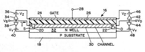
Fig~ 2 illustrates in cross sectlon of an ~ ~-
; 20~ d~a}~lz~ed~-P-channel~MOSFET~whereln an~N-type well 32 lS : .`-
formed ~t~ one~surface~of~ a~P-type substrate la ~ada of
sllicon or other~suitable~semloonductor material ~ Two
relativ~ly-hlgh}y-d~ed,~spaced-apart P+-type reglons 20 and
22 are ~ormed in the surface o~ the ~~type well ~32 and serve
25~ a~ the~source;and~draln r-glons, respoctively, of the ~
MOSFET Ohmlc contracts~S and D~ are;formed on the source 3 '`,'
reglon~20 and~the draln~rogion 22, respectlvely, and form
~m~ part- of~th-~souroe and drain electrodos, to which V5 and VD
are respactively~appl~led ~ ~ gate electrode 2~ ~ade of an
~appropri4t- conductive ~aterial, suoh~as polysilicon or
W O 94/1l903 PCT/US93/Og727 ~ !,
21492~0 1 0
~etal, is formed o~er a thin~layer of insulating material
26, such 85~ sllicon dioxide. This insula~ing layer 26
overlies the surface of the N-type well 32 betwe n the ~ ,
source region 20 and the dr~in reg1on 22. When a negativ~ ' ,"
5~ bias o~ sufficient magnitude is applied to the gate
electrod-~24, the~resulting~electr1c field inverts the
surface beneath~the gate~ electrode~creating a P-type channel
30~which~extends~;between the~P-type source and drain regions
20 an~d 22.~ he creation~o~ the channel 30 allows~a current
lO to flow;betwee~ the source~and drain electrodes S and D, as -~
~; ~ indicated by the arrow labelled ~}n.
In~accordance w1th the invention, the source ~'
electrode~S~ls;coupled to~the end of the~gate~electrode 24
adjacent the source region~20 through a unity gain buffer 34 '''
; lS~ of known~;design~and a level shifter 36, represented in the
example as~a battery, for providing a nagative of~set
voltago~;-V~z bet~een the~end~of the gate electrode 24
'adjacent the source~region 20'and the~source region. The
ctrode~is,~also;coupl~d to the~por~ion of the N-
20~ ~type'~we,11~32~adjacent~the~ source region 20 through a seccnd
unity gain~buffer~38~of known design and a level shifter 40,
represented~in~the~exa~ple as a ~attery, for providing~a ,`
~ ~ ,
posLti~e voltage~of~set~Vy between the portion of the N-type ",',
w~ll 32 ad~acent the source region 20 and the source region.
25~ Si~ilarly,~ the drain ele trode D is connected to the end o~ ~
he~gate~electrode~24 and the portion of ~he N-type well 3'~ ~ '
adj~acent the~drain region 22 through respective unity gain ~ ~
bu~fers 42 and 44j~and associated level shifters 46 and 48, ~ '
represented~by batterLes, for providing a n~ga~ive offset
;3Q ~ voltage -V~ betweqn the end o~ the gate electrode 24
WO 94/11903 ~ 2 1 4 9 2 5 0 ~ PCr/US93/09727
~ ~ ,"'.
:.,
adjacent the drain region 22 and the drain regionr and a
positive voltage:offset Vy~ between the portion of the N-type ,'
, well adjacent the drain reglon 22 and the drain region. '~
This arrange~ent causes the source-to-drain voltage drop Vs~ ,,
5 VD ~t appear~not::only~across~the channel 30, but also across ..
the length of the gate electrode 24~;and across ~he portion "'
of the N-type~well 32 beneath the channel.: ~Beca~se~the ,.'
voltage~:drops along the channel, tha gate electrode and N- .,',
type we~ are~each~ substantia~l~ly llnear~along their ~,,"
l0 ~respectlve lengths~, the~channel-to-gate and body-to-channel ,'~.
: :potentials are maintained~constant along the entire length
of~:the channel.:~ In:this manner, variations in ths number cf .,
carriers,,~ carrier mobility variations and the body effect in 5'
he chan~el~is~ substantially aYoi~è~,~and a linear channe1 ,~
l5~ esistance in:V5 and ~D is:achieved.~
,Thl~ C~n be~de~onstr ted:wlth the ald of the
schemat~ic~diagram cf~Fig~. 3 whlch represents a circuit model --.
,of::~th-;~arrang~ent of~ Flg.~2 and whereln llke parts ~are
d lgnatèd by:the~sa~e~re:ference nu~erals. ~eferrlng to~ ~,
2~0~ Flg.:3,~the gate~and~body~resistanc-s of;~the~;~OSF~T are each '".
repres~ented~by~a~:~r~spective~one-dimensional distributed~
: resistancè;of:constant~resi:stivity. ~Thes2 distributed :
: resistances have ~qual leng~hs, L, corresponding to the
: leng~h of channel~30.~ The leftmos~ end of each of:~hese ~"'
25~ resistances~ia~designa~ed~x = 0, a~d thi:right~ost~end~is
deslqnated x -~L-~ ~The~gate voltag e VG~ the channel voltage
: Vc~and~b~ody~vo~ltage~V8 a~:any selected point x along the
length of~the~channel~,may each be expressed as a function o~ ~ '",.^
, x,.as foll,ows~
WO 94/tl9~3 2 1 4 ~ P~/US93/09727
.,
:
VO(X) = VS_VZ+L(VD_VS)~
x
~V8(x) = V5+vy + L (VD~-VS~ and (2) ~:
, "
X): =:VS+ L (VD_VS~ 131
where equation (3) assumes that ~the voltage VcH(X) -Vs varies
: linearly along the length ~ of the channel. Subtracting
egUatlon~3)~frp- each~o~ -qUatLon (~1) and 2gUation (2)
V~ ~X) -V~D(X~ = -Vz; nd ~ (4)
S~ which~ de~nonstra~es that :~G-Vc~and~-~VB-VcE~ are constant : 1~
throughiout the~:length: of the: :channal. ~ :The ~resistance of the -:
chann~ 30 ~ay~ b~:~ tuned~ by ~arying the offset: voltages. Vz
The:devica~of;;Flg. 2 is pr~ferably fabricated in
~planar ~echnology. :Because in a planar::technology:the
: contact: to: the: q~t~, channel and body canno~ be positioned :.
in the mann-r ~sho~: ~in :Fig. ~ 2, ~these contacts are
advant~geously~formed:on~the~upper surface of t~e de~ice. '~
In the~physical layou~ shown in Fig. 4, th~ spaced source
15 ~and~drain regions 2:0 and 22 ar~ fo ~ ed in:the upper surface `.
of~t~e N-type~wel1~:32. The opposite end~ af gate electrod~ ~
~ W 0 94/119~3 2 ~ ~ 9 ~5 ~ PCT/US93/09727 ~ '
1 3
.
,
~: . . ~,'
24 partially overlap, bu~ are not in electrical contact
with, the source~and drain regions 20 and 22. The gate ~:
electrode, which in the exa~ple is T-shaped at both ends, is
separated ~rom the N-type well 32 by a layer of insulating
5 ma~erial 26, which overlies the surface of the well between ::
~ , :
the source and drain reglons 20 and 22. Two pairs of
contact windows l and 1', are formed at the ends o~ gate
elec~rode 24:adj;acent to the~source and drain regions 20 and
22, respectively.~ Contact windows 2 and 2' are formed over
:: 10 the source and drain regions 20::and 22, respectively. A
pair~ of contaot windows 3 straddling the source region 20,
and:~a pair of~contict windows 3i straddling the drain reqion -.
22:~are formed~over the~portions~of N-type well 32 which are
:adjacent to the source and drain regions, respectively. A
15 ~ f~irst pa~ir~o~:metal conductors 13 and 13' ar~ connected via
respective~contact~wlndows l~to~opposite ends of the "T" at i,
: the~end o~f;the:~gate:electrode~;~ad]acent the~source region 20,
and~a~second~pair~of~meta~l conductors 14 and 14' are
:conne¢ted via~r2spèctive contact windows l' to opposite ends
o ~- ~o~ the "T"~at the~end of~the ga~e electrode adjace~t the '.
dr~in~r2~ion 22.~Although not sho ~for the saka of ~ ...
simplici~y, conductors 13 and~13' are~ electrically connected
: together:by known techniques (e.g., crossiovers or -
: : crossun~ers),: as are~conductors 14 and 14'. Two pairs of . .-~
25 ~ metal conductors ore~connected to the w-ll 32... One pair 5 : ~y
and~5'~ are connected to~the portion of the~well adjacent the
source~:region 20~via:respective contact wlndows 3 s~raddling
- : the connection~o:f metal conductor 11 to th- source region,
and a second pa:ir ~ and 6~ is connected to;thei portion of
30~ the well ad~acent the drain region 22 via contact windows 3'
W ~ ~4/11903 PCT/US93/09727~
~1492~
. straddling the connection o~ metal conductor 12 to the drain
region a2. Conductor pairs 5 and 5' are elec~rically~ . ,'.
conn~cted;together by knawn teGhniques, as are conductors 6 ' ''~'
and 6'.~ Th~alternative arrange~ent shown in Fig. S has~,,',
5~: three well, contacts at each end of the channel, two'.~:,
straddling the source;or~;draln region~and a~ third located
outboard~from~the~source or~drain, the three con~acts at:~'
acn~end:~being~electrically~connected:together as shown, ,.'
Other:contact~arràngements~may:be used~by those skilled in
lO~ the~art~in~accordanG-~with~the~ lnvention. Advantageous .-'.
locatlons of~ith-~contaots ~ay be:dètermined experimentaliy ~,
or~through~kno~ three-dimensiona}~computer slmulation of ; '.
he~structure~shown in~Fig. 4 is connected to
15~ the~driviing~circuit~in~the~manner shown in Fig. 4A. The '-.
;source~e~lectrode~S~of~he~deYice is~conne~oted through the ~:
;bu~ier~34~and::the~ vel~:~shifter~36 to~ he;yàte conductors 13
. a*d~ 3'~ ;The~source~elei ode~:~S~ is:~also~con ected through :
the~buffer~3~8~and~:~the~1~vel shifter 40 to th~ well
2~0~;c ct s~5~ a ~5';~ Simllarly,~ tha drain~electrode~D~of
the~dévice~'is;~conn~e7ted~through the buffer ~2~ and the level
sh~ifter:~46~to~the,~gate~.conduc~ors:~14 and 14'. The drain
electrode D is also connected through the~buff7er 44 and the .
level shi~ter:48~to the well conductors 6 and ~
25~ E'ch~of:~tha,~pa'rJ;~of buffers (34, 3a and 42,:44)~ : ~ .. '
ccupled~to~apposite~ends~;o~ thQ~channel, as shown in Fig. 3, '
may~:be replaced~with~a~single` buffer, as shown in Fig. 6.
That~is,~the~source eIectrode~S ~ay be connec~d to the ; .
inpu~ o~ a:singl`e~unity~gain buffer 80, instead o~ t~e ~wo ~ ~'
30':~ ~shown in Fig.~3. The~output of the buffer 80 is then
~ W ~ 94/11gO3 2 1 ~ g 2 S ~ P~TIUS93~9727
" ~ ,
....
: , . . .
~; coupled to the end of the gate electrode and the portion of
the N-type well adjacent to the source re~ion thxough level
shifters~36' and 40', respectively. Similarly, the drain
electrode D may be connected to the input of a single unity
gain buffer~2.; The output of th~ bu~fer 82 is then coupled
to~the end of the gate el~ectrode and the portion of the
N-type well ad]acent to~the drain region through level
shifters-46'~and 48',~respeGtively. In special applications
where 1t~ls~not~required~to~sense the channel current at one
: lO end of the channel, the buffer or buffers at that end can bs
omitted altogether. ~
:The bu~fer~and~level shifters in the~disclosed -,`
embodimenti of;the~ nventlon may~be conv ntional circults
for~providing~théso ~unctions to ach1eve the desirod channel
15~ linearity.~ Furthe ~ ore,~;it~ lS dos1rable~that the buffer and
: Ievel~shlft~er cirruits used~:be ~apable of b~ing integrated
:in tho sa~è~semioonductor ohip~as:the:f1eld-ef~eo~
transis~or:device:~whose channel resistance:is bein~ '
linaarize~ A~ong known~circuit techniques:for the buffer c-
20~:~ and~lev~ shifter ~unction~for the-voltag~ Vy is the emitter
oll~ower shown in Flg.~ 7A, in which tho oolleotor of an NPN
bipolar transistor ls, for;example, connected tb a voltage
source ,VDE,: and the :~ase is connected to the voltage V~ at ::-
the source electrode:S so as to produca at 'he emitter
25~:~ output,~ a potontial Vsfvy, ~ where Vy lS the emitter-to-base '- ~:
vol~a~e of: the transistor in the actiYe region of o~era~ion.
sihllar circuit su1tahl-~for the purpo~e i5 tho Darlington
pair:em:itter follower~shown in Fig. 7B, which produces at
:th- e~ittor~output a potential vs+vy~ where Vy represonts ~-
30:~: tw~ ~mitter-to-base voltage drDpS.
WO94/11903 ~ PCI/U593/097Z7~ ¦
2 1 ~
1 6 -:
: Another~known technique is the hybrid MOS-bipolar
follower~circuit shown~in Fig. 7C arranged to produce a
: voltage shif~ Vz, in which cascaded bipolar transistor -:
followers:are dr1ven by an ~OS trans1stor having its gate
5; ~connected to:~the voltag~;V5 at the souroY~electrode S. This ;~
circuit produce~an~o~fæet voltage~Vz equal to the sum of
the~gate-to-souroe~voltage;of the~MOS stagY and ths base-to-
;emltter~voltages~of~thY:bipolar transistors. A sufficient - -
` number~ of~ ~bipolar ~transistors~can :bY used to provide the
: 10 desired offset. Varying the~current through the MOS stage
:varies the value;of Vz for t~ning the channel resistance of .-.
the~devlGY.~
; ThY~ ~ :fYr and:le Yl sh1ftYr m~ay also~;be
implementYd~us~lng~an~operational amplif~ier of convent~ional
S~ des;ign~ as~sho~ ln Fig~.~:7D~ RefYrring~to Fig. 7D the
voltage~ at~the~souroe e e e~S is applied to the~ ;
having thi~;`indicab:ed~polarity~is:co ~ ed fr ~ the output
t~the inverting:input;~to produce an output voltage Vs-V~. -
0~ ThY~vol:ta
depend~nt~voltagé~drop across~:a rasi~tor or trans1s~or
wherè the~current through the dévic~ may be varied to change
z for tu m ng the ~fhann-l resistance of the ~ield-~ffect
transistor~:resi:;tance~:d~evice.
25 ~ It~ be~understood~tbat~the oircuit~of~Fig~.
7A-D~ ~which~i~have~been~described as providing the offset
:;voltaq~Vz~between;~the~source and drain regions and the ends
of:the~gate~:electrode~adjacent to the source and drain
regions~ respec~ively, are also equally applicable for
3a~ providing the:offsot voltaqe Vy botwoon the ~ource and drain ~
~ W 0 94/11903 2 l ~ ~ 2 5 0 PCT/US93/097~7
1 7
."
regions and respective portions of the body adjacent to the
source~and~draln regions, with appropriat~ modifications~;
known to those~akilled ln the art
Yet~another known unity-gain;buffer and level
5~ ~ahi~t-r~circult~suitable for providing offset voltages
between èhs sour~e and drain~r-glons, and the ends of ~he
gate~ electrode~and~the~portlons of the body adjacent the
source~;and~drain`~reglons,~ r~espectively, is the circuit shown ;-~
in ~Fig. ::8~. ~ This~-circuit consis~s~ of two pairs~of~MOS
10 ~ transistors, Tl, T2 and T3, ~T4, ~each connected in series
with~à respective current source so and 92 between supply
voltages +VDD~and~-VsS ~The gate of Tl is~oonnec~ed to the
common node~of T3~ and T4~,~while the gate~of T3~ is oonneoted
to~the~common nod¢~of Tl~and~T2~ The voltages at the source
15 ~ and~drain~ electrodes~, Vs and~VD, of the~field-effeot
t n stor reois anoe~ vioe~a~ap lied to the gates
and T4,~espectively`,~and~shifted voltages Vs + Vy and VD +~
Vy are proYided~at~the~sourc~ ter~inals o~T3~ and~
r-sp-cti~ely ~The~offs-t voltag- Vy~may~b-~expressed by the -~
20 ~ followin~ -r-~lationshi
; wh-re V5c i~s th- sour=e-to-gat~ voltag- or Tz and T3, or a~
and T~ is th-~curr-nt~through~ T1 and T2, and I3 is the
cu~rent~through~T3 and~T4;~ That is,~the~shifts of V5 and VD~
;ar-~equa;l~;aJ~r-quir~d Other oircuits using MOS or bipolar ?
; 2;5~ d-vlces, ~or-~co~bina~ions~of device typ-~,~will be known to ~ -~
those sk~ll-d;~n the~art;~or providlng th- required
W O 94/~1903 2 1 ~ 3 2 ~ D PCT/USg3/0 7 ~1 ,
l 8
: : ''''
buffering and level shLftlng function~ in accordance with
t~e invention
While the invention has been described with ---
re~erence to oevera~l exe~plary embodiments thereof, it will
5 bé understood by those skill~d in the art that various
changes in for~, d-tail~ or design may be made therein
~ithout departing from the spirit and scope of the
invention For eYample, ~the field-effect transistor of the
;reslstance device may be of a depletion type, in which cas
Vz would be of the-opposite polarity, or the trans~istor may
be an N-channel devlce where the body region is p-type, and
the~sou~ce and drain regions are N-type se~iconductor
material ~ Moreover,~the f~ield-~f~ect transistor need not be
of~th- insulated gate type but may instead be a ~unction ~-
15 ~ field~-ffect~transistor (JPET~where the gate e}ectrode is a
;sùrface region of one conductivity type formed in a channel ~-
region o~ th~ opposite conducti~ity ~ype, and at the ends of
the~chann-l~r-gion~th- Jource and~drain regions are of the
opposit-~onductivity type, and the~body region opposing the
20~ gate~-lectrode lS of~th- one~conductivity type If the
field-e~fect~transistor is a J~T, Yz and Vy have the same
p~larity~
~ ~ ;: ~ : : .:
~ ~ , . : . .